http://dx.doi.org/10.6113/JPE.2014.14.1.22 ISSN(Print): 1598-2092 / ISSN(Online): 2093-4718
JPE 14-1-3
Improved Droop Method for Converter Parallel
Operation in Large-Screen LCD TV Applications
Jung-Won Kim
*and Paul Jang
†*
Engineering Research Institute, Seoul National University, Seoul, Korea
†
Department of Electrical and Computer Engineering, Seoul National University, Seoul, Korea
Abstract
Current sharing between modules in a converter parallel operation is very important for the reliability of the system. This paper proposes an improved droop method that can effectively improve current sharing accuracy. The proposed method adaptively adjusts the output voltage set-point of each module according to the current set-points. Unlike conventional droop control, modules share a signal line to communicate with each other. Nevertheless, since signals are simple and in digital form, the complexity of the circuitry is much less and noise immunity is much better than those of conventional methods utilizing communication. The operation principle and design procedure of the proposed method are described in detail. Results of the experiment on two boost converters operating in parallel under the specification of a TFT LCD TV panel power supply verify the validity of the proposed scheme.
Keywords: Adjusting output voltage set-point, Current sharing, Droop method, Parallel operation
I.
INTRODUCTION
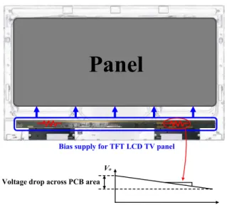
With the rapid development of technology, switched mode power supply has been optimized for industrial demands. The major design trends of products are shifting toward larger and thinner displays, especially in the thin-film transistor liquid crystal display (TFT LCD) TV panel market. As display sizes continue to increase, maintaining a stable output voltage with high accuracy throughout the entire panel gets harder because voltage drop across wide printed circuit board (PCB) area increases. Designing small-sized, high-accuracy TFT LCD power supply circuits has thus become an important issue in product design. The parallel operation of DC-DC converter modules can be a solution to this problem by supplying highly accurate localized voltage across a wide PCB area. Normally, paralleling DC-DC converters provides great flexibility to systems because of the expandability of output power and the improved reliability because of its redundancy [1]. In TFT LCD applications, it can also offer stable output voltage throughout a large area in particular.
When several converters are operated in parallel, uniform current distribution among modules is a major concern
Bias supply for TFT LCD TV panel
x Vo
Voltage drop across PCB area
Panel
Fig. 1. Voltage drop across a wide PCB area in a large TFT LCD TV.
regarding system reliability. Unless the current is distributed uniformly, the module where high current flows can suffer from high temperature rise and system reliability would deteriorate. Many current sharing methods have been proposed and verified in previous studies [2]-[13].
One of the commonly employed methods is interconnection-based current sharing control that utilizes a Manuscript received Sep. 6, 2013; revised Oct. 17, 2013
Recommended for publication by Associate Editor Joung-Hu Park.
†Corresponding Author: [email protected]
Tel: +82-880-1785, Fax: +82-878-1452, Seoul Nat'l University
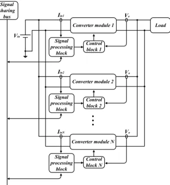
Load Vo Vin Signal sharing bus Signal processing block Signal processing block Signal processing block Converter module 1 Converter module 2 Converter module N Iin1 Iin2 IinN Vo Vo Control block 1 Control block 2 Control block N
Fig. 2. System block diagram of the proposed method.
communication link between converters for parallel operation [2]-[7]. Although this method offers accurate current sharing and output voltage regulation, it requires high-speed communication and offers less reliability due to single point of failure.
Another widely employed method is droop-based current sharing control, which is the simplest method to implement because no communication link is required. This method only relies on the internally and/or externally added resistance of the parallel modules to maintain a relatively equal current distribution between modules. However, since current distribution is achieved at the expense of output voltage regulation, the droop control method cannot satisfy these objectives simultaneously [8]. Several methods have been investigated to overcome this problem [9]-[13]. As a part of these researches, this paper proposes a new method based on droop control for converter parallel operation, which adaptively adjusts the output voltage set-point of each module according to the current set-points. Unlike conventional droop control, modules share a signal line to communicate with each other. Nevertheless, since signals are simple and in digital form, the complexity of the circuitry is much less and noise immunity is much better than those of conventional methods utilizing communication.
Research on modifying droop characteristic has already been conducted in [11]-[13], some studies [11], [12] made the slope of the droop method steeper to improve current-sharing performance which is the key difference from the proposed method in this current study. None of the previous studies analyzed their scheme from the perspective of current
1 set I Iset2 Iset3 ( 2) sp V (1) sp V ( )n I step V D ( ) o n V
Fig. 3. Droop characteristic of the proposed method.
sharing.
In [13], the output voltage set-point of the converter was adjusted by a digital signal processor (DSP) depending on the magnitude of the circulating current. However, it is only applicable to converters utilizing a synchronous rectifier while the proposed method is applicable irrespective of adapting a synchronous rectifier.
This paper is organized as follows. Section II provides a description of the operation principle of the proposed method. The design procedure of the proposed method under the specification of a TFT LCD TV panel power supply is introduced in Section III. A detailed simulation and experiment are performed to verify the validity of the proposed scheme. The results are shown in Section IV. Section V provides the conclusion.
II.
OPERATION PRINCIPLE
A new method based on droop control is proposed in this study to achieve current distribution and output voltage regulation simultaneously. Contrary to other methods that modify the droop characteristic, the proposed method adjusts the output voltage set-point of each module instead of making the slope of the droop steeper. In this scheme, some specific current set-points are selected in advance. When the current value of the highest current flowing module reaches these set-points, the module sends a digital signal to the other modules to adjust their output voltage set-points. Any module that has ever sent a signal does not respond to signals from the others and any module does not generate a signal at the same set-point more than once. Otherwise, all the droop characteristics would go upward continually. When all the modules have generated at least one signal, the output voltage set-point adjusting process is terminated. When a module that has never sent a signal exists, it will be carried out until the highest current set-point is passed by. The parallel operation of two converters is described in this study. However, the proposed scheme is applicable for a higher number of converters in parallel.
Fig. 3 shows the basic operation principle of the proposed method. The output voltage set-point of module 1 is higher than that of module 2, therefore module 1 supplies the entire load current before its current reaches Iset1. When the current of module 1 reaches Iset1, it sends a digital signal to module 2 to shift the output voltage set-point of module 2 upward. Simultaneously, the output voltage set-point adjusting circuit of module 1 is forced to ignore any signal from other modules. Otherwise, the output voltage set-point of the two modules would increase continually while generating and receiving signals with each other. The module that has sent a signal remains unchanged by a signal generated by other modules to prevent this event. If the output voltage set-point of module 2 shifts upward, the load current begins to be supplied by both module 1 and module 2. As the load current increases further, the module 2 current reaches Iset1, but module 2 does not send a digital signal to module 1 because the signal processing circuit of module 2 is forced not to generate a signal. If module 2 generates a signal by Iset1, it cannot respond to any signal generated by other modules afterward because the module that has sent a signal previously remains unchanged by the signal from other modules as mentioned above. As the load current increases further, the current of module 1 reaches Iset2, then module 1 sends a signal to module 2 to shift the output voltage set-point of module 2 upward again. As a result, the difference between the two modules is reduced. After Iset2, the higher current flows through module 2 because the output voltage set-point of module 2 is higher than that of module 1. When the current reaches Iset3, module 2 also sends a signal to module 1. At this point, however, module 1 does not respond and the adjusting process is terminated. In consequence, the droop characteristic of the proposed method is summarized as follows:
( ) ( ) ( )
o n sp n n step
V =V - ×k I +m× DV (1) where Vo(n), Vsp(n), and I(n) are the output voltage, the output voltage set-point, and the input/output current of the nth module, while k, m, and △Vstep are the droop gain, the number of adjusting events, and variation amplitude of the output voltage set-point when one adjusting step occurs, respectively. Since either the input or output current of the modules can be used for the droop method, I(n) stands for both.
III.
DESIGN PROCEDURE
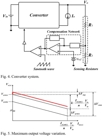
Fig. 4 shows a general representation of the converter system. The output voltage set-point of the system can be determined as 1 2 2 sp ref R R V v R + = . (2)
Fig. 4. Converter system.
max sp V ( ) in n I max o V D max sp V D ( ) o rate o in I V k n V × × ( ) o rate o in I V n ×V ( ) o n V min sp V step V D
Fig. 5. Maximum output voltage variation. TABLE I
SYSTEM PARAMETERS FOR A TFTLCDTVPANEL
Input voltage (Vin) 12V
Output voltage (Vo) 17.5V
Rated output current (Io(rate)) 500mA Output voltage regulation (△Vo max) ± 0.3V
Equation (2) shows that in the parallel operation of the converters, the output voltage set-point difference between the modules, △Vsp, mainly originates from the error of the sensing resistance and reference voltage tolerance of the controller. For instance, we assume that sensing resistors R1
and R2 and reference voltage, vref, have ±1% error tolerance. Then, the maximum output voltage set-point difference between modules, △Vsp max, is approximately 6% of the output
voltage if Vo >> vref. This difference causes current unbalancing of max max sp V I k D D = . (3) By shifting the output voltage set-point of a low-current module upward, current unbalance between modules can be improved as follows:
max max sp step V m V I k D - × D D = . (4)
As more adjusting steps are introduced, more accurate current sharing is attained. However, the output voltage set-point adjusting network would require additional components, and the entire circuit would become complicated. Therefore, the number of steps should be deliberately selected considering current sharing accuracy and circuit complexity. This design procedure is discussed in detail by employing two boost converters under the specification of a TFT LCD TV panel power supply as shown in Table I. The input current is used for droop characteristic instead of the output current in the following procedure.
A. Selecting △Vsp maxand △Iin max
Table I shows that △Vo max is ±0.3V in the design procedure. The worst case should be considered to satisfy this output voltage regulation. The maximum output voltage occurs when Vsp(1) and Vsp(2) are almost similar around the maximum output voltage set-point, Vsp max, and one adjusting event occurs. The minimum output voltage occurs when Vsp(1)
and Vsp(2) are almost similar around the minimum output voltage set-point, Vsp min, at full load condition. As shown in Fig. 5, the maximum output voltage variation, △Vo max, is determined by ( ) max max o rate o o step sp in I V V V k V n V D = D + × × + D . (5)
Considering the voltage drop caused by droop gain, selecting △Vsp max as 1/3 to 1/2 of △Vo max is recommended. In this case, △Vsp max is assumed to be 0.2V.
After selecting △Vsp max, the desired output current sharing
error is selected next. Although it depends on the design principle, designing △Iin max to be approximately 10% of the
rated input current is recommended. In this design, △Iin max is selected as 70mA.
B. Determining the number of adjusting steps m
The number of adjusting steps can be determined based on the above designs. The number of adjusting steps should be deliberately selected for a trade-off between current sharing accuracy and circuit complexity. By selecting the number of adjusting steps, △Vstep is obtained as
max sp step V V m D D = . (6) In this design, m is determined as 4. Thus, △Vstep is 0.05V.
C. Selecting droop gain k
Once allowable △Vsp max, △Iin max, and m are selected, the
droop gain can be selected based on two conditions.
First, △Vo maxis determined by k, △Vstep, and △Vsp max from
(5). Hence, the desired droop gain condition is obtained as
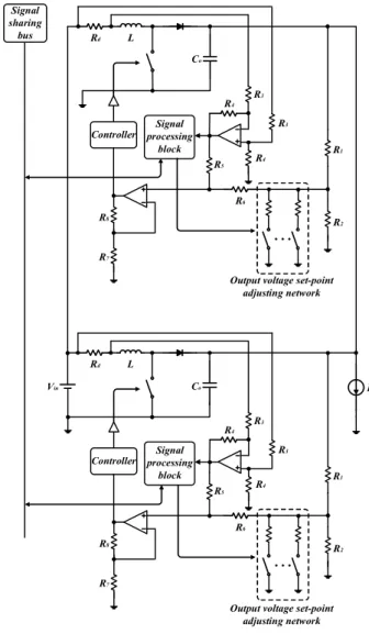
Signal sharing bus Controller Co R5 R7 R4 R8 R6 Rd L Co Rd L Vin Io R2 R1 R3
Output voltage set-point adjusting network R3 R4 Signal processing block Controller R5 R7 R4 R8 R6 R3 R3 R4 R2 R1
Output voltage set-point adjusting network Signal
processing block
Fig. 6. Circuit implementation of the proposed method.
max max ( ) o step sp in o rate o V V V V k I V n D - D - D £ × . (7)
Current sharing accuracy is determined by △Vsp max, △Vstep, and k from (3) and (4). The worst current sharing occurs when two droop characteristics are almost same at first, then one adjusting event occurs. From this worst case, we can obtain another droop gain condition as
max max sp in V k m I D ³ × D . (8)
Droop gain k should be designed to satisfy both (7) and (8). In this design, k is designed as 0.86.
D. Circuit implementation
An implementation of the proposed method is shown in Fig. 6. Current sensing resistor Rd, which is connected in series with an inductor, is utilized to realize the droop gain k.
Fig. 7. Operation of signal processing block when module 1 sends signals to module 2. Iin1 Iin2 146 in I mA D = 163 in I mA D = 101 in I mA D = 37 in I mA D =
<Iin1>avg
<Iin2>avg 1st adjusting 2nd adjusting 3rd adjusting 4th adjusting
Fig. 8. Simulated waveforms of the input currents of the two modules.
As a result, k can be expressed as follows:
6 7 8 4 1 2 3 2 5 6 7 d R R R R R R k R R R R R R æ ö æ ö æ + ö + = ç ÷ç ÷ ç ÷ + è ø è ø è ø . (9)
A non-inverting summing amplifier is employed to implement the droop method by adding output voltage and input current information.
Adjusting the output voltage set-point is realized with switches and resistors that are connected in parallel with sensing resistor R2. If the output voltage set-point adjusting network receives a digital signal from the signal-processing block, one of the switches is turned on by that signal. The resistor that is in series with the turn-on switch is then connected in parallel with R2, and the sensing gain of the
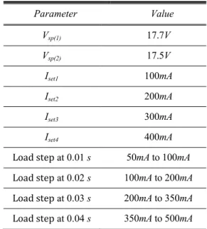
TABLE II SIMULATION PARAMETERS Parameter Value Vsp(1) 17.7V Vsp(2) 17.5V Iset1 100mA Iset2 200mA Iset3 300mA Iset4 400mA Load step at 0.01 s 50mA to100mA Load step at 0.02 s 100mA to200mA Load step at 0.03 s 200mA to350mA Load step at 0.04 s 350mA to500mA
signal-receiving module is reduced. As a result, the output voltage set-point of the signal-receiving module moves upward.
The signal operation of the proposed method is shown in detail in Fig. 7. Whenever the sensed input current becomes higher than a certain current set-point, the comparator relevant to that current set-point generates a step signal and it is converted to a one-shot pulse by a leading edge detector block. Generated one-shot pulses are gathered through an OR gate, and a single digital signal is sent to the signal-receiving module. At the signal-receiving module, the number of pulses is counted by the counter block and a corresponding number of switches are turned on in the output voltage set-point adjusting network. The counter ignores any pulse generated by itself.
IV.
VERIFICATION RESULTS
A. Simulation Results
A simulation is conducted to verify the effectiveness of the proposed method. A system of two boost converters operating in parallel is designed based on the specifications in Table I. The simulated conditions are listed in Table II. There are four current set-points. Whenever the average input current of the module with the higher flowing current reaches these set-points, the module sends a digital signal to the other module to decrease the difference between the output voltage set-points. The values of the load steps are determined to go over current set-points for each step change.
Fig. 8 shows the simulated input currents of the two modules. Initially, module 1 handles the entire current because Vsp(1) is higher than Vsp(2). Although the first output voltage set-point adjusting operation occurs at 0.01 s, module
1 still supplies the entire load current because △Vsp is still large. After the second output voltage set-point adjusting operation occurs at 0.02s, the load current begins to be supplied by both modules 1 and 2. At this point, the input current difference between modules 1 and 2, △Iin, is 163mA.
As the third and fourth load current step changes occur, △Iin
decreases to 101mA and 37mA, respectively. These results show that the input current difference between the modules is reduced successfully through the proposed method.
B. Experiment Results
A prototype of the two boost converters operating in parallel under the specifications in Table I is constructed following the design procedure to validate the above operation principle and simulation results. The circuit parameters of the prototype are shown in Table III. The load step time of the experiment and simulation is different because performing a long time simulation with limited maximum memory is difficult.
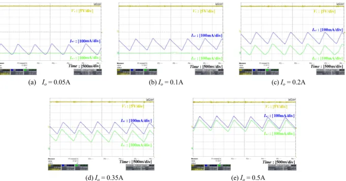
Fig. 9 shows the measured waveforms of the experiment. Channel 1 is the output voltage, channel 3 is the average input current of module 1, and channel 4 is the average input current of module 2. The load current sequentially steps up from 0.05A to 0.1A, 0.1A to 0.2A, 0.2A to 0.35A, and 0.35A to 0.5A. It then steps down in a reverse order. Similar to the simulated condition, the values of the load steps are determined to go over the current set-points for each step change. The entire current was supplied by module 1 before
TABLE III
CIRCUIT PARAMETERS OF THE PROTOTYPE
Parameter Value L 20mH Rd 0.068W Co 10mF R1 100kW R2 7.5kW R3 2.2MW R4 2.5MW R5, R6, R7, R8 1MW fsw 1.2MHz
the average current of module 1, <Iin1> avg, reaches Iset2
because the output voltage set-point of module 1 is higher than that of module 2. After the second adjustment, △Iin
gradually decreased as <Iin1> avg passes Iset3 and Iset4. As a
result, although △Iin after the second adjustment is 169mA, it decreased to 25mA finally. The output voltage set-point adjusted once remained unchanged, while the load current decreased. Therefore, the stepping down of the load current in
51
in
I mA
D = DIin=120mADIin=169mADIin=96mA DIin=25mA DIin=30mA DIin=34mA DIin=38mA DIin=20mA
Fig. 11. Measured droop characteristics of each module.
a reverse order has a trivial effect on △Iin, and improved current sharing is almost maintained continuously. The minor differences shown in the step down sequence mainly originate from approximately 6% of the mismatch between the k values of the two modules.
Fig. 10 shows the enlarged input current waveforms of both modules in the load step up sequence. △Iin is effectively reduced as the load current increases. The output voltage is 17.65V when Io is 0.05A and 17.35V when Io is 0.5A. Thus, the required voltage regulation of ±0.3V is effectively satisfied by the appropriate design of droop gain k.
Fig. 11 shows the measured droop characteristics of each module. Initially, the output voltage set-point difference between the two modules is 185mV. However, the difference
gradually decreases as adjusting events occur and finally becomes 11mV after the 4th adjustment.
V.
CONCLUSIONS
In this paper, an improved droop method that can effectively improve current sharing accuracy is proposed. The proposed method adaptively adjusts the output voltage set-point of each module according to the current set-points. Unlike conventional droop control, modules share a signal line to communicate with each other. Nevertheless, since signals are simple and in digital form, the complexity of the circuitry is much less and noise immunity is much better than those of conventional methods utilizing communication. The operation principle and design procedure of the proposed method are provided. Following the design procedure, a 17.5V/500mA prototype of two boost converters operating in parallel was constructed. The experiment results show that the input current difference between the modules was successfully reduced through the proposed method.
REFERENCES
[1] S. Luo, Z. Ye, R.-L. Lin, and F. C. Lee, “A classification and evaluation of paralleling methods for power supply modules,” in Proc. IEEE PESC, Vol. 2, pp. 901-908, Jun. 1999.
[2] S. K. Mazumder, and M. Tahir, and K. Acharya, “Master-slave current-sharing control of a parallel DC-DC converter system over an RF communication interface,” IEEE Trans. Ind. Electron., Vol. 55, No. 1, pp. 59-66, Jan. 2008.
[3] Y. M. Lai, S.-C. Tan, and Y. M. Tsang, “Wireless control of load current sharing information for parallel-connected
Vo: [5V/div]
Iin1: [100mA/div]
Iin2: [100mA/div]
Time : [500ns/div]
(a) Io = 0.05A (b) Io = 0.1A (c) Io = 0.2A
(d) Io = 0.35A (e) Io = 0.5A Fig. 10. Input current waveforms in the load step sequences.
DC/DC power converters,” IET Power Electron., Vol. 2, No. 1, pp. 14-21, Jan. 2009.
[4] J.-J. Shieh, “Peak-current-mode based single-wire current-share multimodule paralleling DC power supplies,” IEEE Trans. Circuits Syst.Ⅰ: Fundam. Theory Appl., Vol. 50, No. 12, pp. 1564-1568, Dec. 2003.
[5] M. Lopez, L. G. de-Vicuna, M. Castilla, P. Gaya, and O. Lopez, “Current distribution control design for paralleled DC-DC converter using sliding-mode control,” IEEE Trans. Ind. Electron., Vol. 51, No. 2, pp. 419-428, Apr. 2004. [6] J. A. Abu Qahouq, L. Huang, and D. Huard, “Sensorless
current sharing analysis and scheme for multiphase converters,” IEEE Trans. Power Electron., Vol. 23, No. 5, pp. 2237-2247, Sep. 2008.
[7] Y. Kanthaphayao, U. Kamnarn, and V. Chunkag, “Redundant operation of a parallel AC to DC converter via a serial communication bus,” Journal of Power Electronics, Vol.11, No. 4, pp. 533-541, Jul. 2011.
[8] B. T. Irving and M. M. Jovanovic, “Analysis, design, and performance evaluation of droop current-sharing method,” in Proc. IEEE APEC, Vol. 1, pp. 235-241, Feb. 2000. [9] J.-W. Kim, H.-S. Choi, and B. H. Cho, “A novel droop
method for converter parallel operation,” IEEE Trans. Power Electron., Vol. 17, No. 1, pp. 25-32, Jan. 2002. [10]A. D. Erdogan and M. T. Aydemir, “Application of adaptive
droop method of boost converters operating at the output of fuel cells,” in Proc. IEEE ELECO’09, pp. I-321-I-325, Nov. 2009.
[11]H.-H. Ho, K.-H. Chen, and W.-T. Chen, “Dynamic droop scaling for improving current sharing performance in a system with multiple supplies,” in Proc. IEEE ISCAS, pp. 545-548, May 2007.
[12]T.-J. Tai and K.-H. Chen, “Switching loss calculation (SLC) and positive/negative slope compensation dynamic droop scaling (PNC-DDS) technique for high-efficiency multiple input single output (MISO) systems,” IEEE Trans. Power Electron., Vol. 24, No. 5, pp. 1386–1398, May 2009. [13]S. Anand and B. G. Fernandes, “Modified droop controller
for paralleling of DC-DC converters in standalone DC system,” IET Power Electron., Vol. 5, No. 6, pp. 782-789, Jul. 2012.
Jung-Won Kim received his B.S., M.S., and Ph.D. degrees in Electrical Engineering from Seoul National University, Seoul, Korea, in 1994, 1996, and 2001, respectively. He was a Senior Engineer in Fairchild Korea Semiconductor, Ltd. He was a Vice President of Silicon Mitus, Inc. from 2007 to July 2013. He is currently a Senior Researcher in the Engineering Research Institute of Seoul National University, Seoul, Korea. His current research interests include power factor correction, converter parallel operation, modular converter systems, distributed power systems, and soft switching converters.
Paul Jang received his B.S. degree in electrical engineering from Seoul National University, Seoul, Korea, in 2010, where he is currently studying for a Ph.D. degree. His research interests include DC–DC and AC–DC power conversion and control.