3170 Archana yelmate*
Assistant professor, Department of Pharmaceutics, Dayanand College of Pharmacy,
Barshi Road, Latur-413531. Contact no: 9822336268 E-mail: [email protected]
*Address for correspondence
Review Article
NANOSENSOR - A COMPREHENSIVE REVIEW
Archana yelmate*
Department of Pharmaceutics, Dayanand College of Pharmacy, Barshi Road, Latur- 413531, India
A RT I C L E I N F O A B S T R AC T
Key words:
Nanosensor, Optical, Mechanical, Electromagnetic
Nanosensors are gaining increasing attention due to the need to detect and measure chemical and
physical properties in difficult to reach biological and industrial systems that are in the nano-scaleregion. Most reviews on nanosensors are focused on a particular type of sensors, such as nanobiosensors, optical nanosensors and magnetic nanosensors with many technical details.This conceptual review surveys various nanosensors, which are categorized into three broadtypes: optical, electromagnetic and mechanical nanosensors, with their advantages and disadvantages along with similarities and differences among the v is to providearious categories. The aim behind this review is to provide an overview on nanosensors which is suitable for beginners to realize the growing importance of the field.
INTRODUCTION
Nanosensor are biological, chemical, surgical sensory points that are used to convey information about nanoparticles to microscopic world. These are used for various medicinal purposes and as gateways to building other nanoproducts such as computer chips that work at the nanoscale and nanorobots & there are several ways utilized to make nanosensors, including top-down lithography, bottom-up assembly and molecular self-assembly. A sensor is a instrument that respond to a physical stimulus such as heat, light, sound, pressure, magnetism, motion. Nanosensor is an extremely small device capable of detecting and responding to physical stimuli with dimensions about one billionth of a meter. Physical stimuli may include Biological, and Chemical substances, displacement, motion, force, mass, thermal and electromagnetic. The main aim behind the development of chemical sensor is to monitor and control environmental pollution, to improve the diagnostics for point care in medical applications.
In the industrial applications, there is a demand for improved sensitivity and stability, which is provided by available sensor. In the emerging field of nanotechnology, sensors play an important role in realizing these goals. The chemical sensors have a wide application spectrum from space mission to homeland security and other application.(34) Nanosensors are the sensing devices with at least one of their sensing dimensions being not greater than 100nm. In the field of nanotechnology nanosensors are instrumental for:
1) Monitoring physical and chemical
phenomenon.
2) Detecting biochemicals in cellular organelles.
3) Measuring nanoscale particles in the industry and environment.
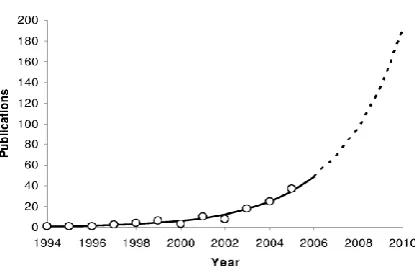
Sensors have a long and illustrious history, the realm of nanosensors is relatively new. The following chart shows the development of various nanosensors within 1994-2005.
The various nanosensors can be loosely grouped into three broad categories of nanosensors:
Optical nanosensors
Electromagnetic nanosensors
Mechanical or vibrational nanosensors
Journal of Global Trends in Pharmaceutical Sciences
Fig 1: Nanosensors within 1994-2005
Many other nanosensors do not fall into above-mentioned categories. Nanoparticles are unique tools as sensors. First, they have the larger size than molecules & now they are smaller than viruses. They are similar to that of many proteins in size & this is the reason that they can operate well inside or within the cells. (36) second nanosensors having unique physical characterstics, they deliver sensitivity order of magnitude better than conventional devices and provided such performance advantages as fast response & portability.(37) Third nanoparticles reveals the unique physical properties which do not in bulk materials. Fourth nanosensors allow for building integrated devices, which provide an elemental base for intelligent sensors. These sensors are characterized as having the data storing, processing, and analyzing power. These sensors are utilized as autonomous system or they spread out in large numbers to form networks. A nanotechnology provides the ability to work at the molecular level, atom by atom, to create large structure with fundamentally new molecular orgnisation. It is concerned with materials, devices & systems whose structures and components having novel and significantly improved physical, chemical, and biological properties, phenomenon and processes due to their nanoscale size.
A nanoscale technology has been developed in NASA Ames by using nanostructures like single walled carbon nanotubes and metal oxide nanotubes or nanowires on a pair of integrated electrodes processed with a silicon-based microfabrication and micromachining technique. The interdigited
electrodes fingers were prepared using
photolithography and thin film metallization techniques. These sensors have been exposed to nitrogen dioxide, acetone, benzene, nitrotoulene, chlorine in the concentration range of ppm to ppb at room temperature. The electronic molecular sensing of carbon nanotubes understood by electron modulation such as charge transfer mechanism, because of charge transfer the conductance of nanostructures will change. The metal oxide nanobelts sensors operate at a lower temp i.e 150oc compared to 500oc for conventional metal oxide
sensor with some sensing behavior. Due to large surface area, low surface energy barrier and high thermal stability, mechanical stability nanostructured chemical sensors potentially can offer high sensitivity. These are more attaractive for defense, space application and also for commercial application. When sensor combined with MEMS technology, light weight and compact size sensors can be made in wafer scale with low cost and high yield. A wireless capability of such a sensor chip can be used for network mobile and fixed site detection and warning systems for military bases.(38)
How nanosensor work:
Chemical nanosensor:
Typically nanosensor work by monitoring electrical changes in the sensor materials.
Ex. Carbon nanotubes based sensors. When molecule of nitrogen dioxide (No2) is present then it will strip an electron from a nanotubes and it causes the nanotubes to be less conductive. If ammonia (No3) is present then it reacts with water vapour and donates an electron to the carbon nanotubes which in turn causes the nanotubes more conductive.
Mechanical nanosensor:
Like chemical nanosensors, mechanical nanosensors are used to measure electrical changes. Those nanosensors that are used in the MEMS systems that car airbags depend upon the change in capacitance.
Examples:
The most famous example of nanosensors which includes the use of fluorescence characterstics of cadmium selenide quantum dots in order to discover tumour in the body. When these small quantum dots are injected into the infected area of human body, then the doctors could determine the exact stage of cancer or tumour. Nanosensors are also used in DNA test to recognize the similar properties of two blood cells.
Advantages:
When the constructions like building, bridge, dams are built then they need to withstand extreme conditions and stand for a long time. In order to detect any such kind of problem scientist have discovered two types of sensors.
The first type is a micro electromechanical system, which checks the temperature and moisture content in the concrete.
Another type of nanosensors developed by our Indian scientists and engineers in order to detect heart attacks or cardiac problems.
Disadvantages:
High cost about 0.6-2.7 billions.
Privacy intrusion.
Security problems.
Medical nanosensors give the future profile about health of an individual along with diagnosis and treatment.
Economic and social impacts of nanosensors:
Nanosensors are still considered as new in the field of nanotechnology. They have a strong economic impact because advance production and high fabrication is required in order to produce nanosensors. The huge cost is required to use this technology. The discovery of properties of specific material is also dangerous because this leads to negative and destructive usages of the substances. Nanosensors also reduced the air pollutions and discovered the strong air pollutants. Nanaosensor technology is relatively a new field. However the nanosensoe developers must overcome the present high cost of production in order to become worthwhile for implementation in consumer products. Ethical and social impacts are hard to define and sort as good or bad by comparing with health and environmental impacts. The advancement in detecting, sensing different biological, chemical species with increased capacity and accuracy may transform societal mechanisms. For ex The ability to measure extremely low amount of air pollutant or toxic material in water raises the questions.
Current nanosensors device:
Nanostructured materials: Ex: Porous silicon.
Nanoparticles.
Nanoprobes.
Nanowire nanosensors.
Nanosystems.
Types of nanosensors:
Depending upon the structure nanosensors are mainly divided into two types:
Optical nanosensor.
Electrochemical nanosensor.
Based upon the application the nanosensors are classified into three types:
Physical nanosensors.
Chemical nanosensors
Biological nanosensors.
Optical nanosensors:
The first developed optical Nanosensor based on fluorescein which is trapped within a polyacrylamide
nanoparticle and which is used for pH
measurements.(1) In this basic concept, fluorescent chemosensors are the molecules which are composed of at least one substrate binding unit (s) and
photoactive component (s).(2,3) The
phosphorescence or luminescence phenomenon means it is a process by which a flurophore absorbs the light of a certain wavelength which is followed by emission of light with an energy corresponding to the difference between ground state and excited state.(4,5) . The fig 1 Show a typical luminescent sensor whereby, the reflected light changes the colour when the receptor binds with analyte that change in photo-vibrational properties that underlines the sensing concept. The most basic optical nanosensor whereby, is like that of the molecular dye probe i.e inside the cell, which is a direct cell loading of fluorescent dyes. (6) A slightly different deviation from this free dye method is the labeled nanoparticle that consist of receptor molecule attached to the outside of the nanoparticles.(7,8) The major difference between the labeled nanoparticles and the free method is labeled nanoparticles having solid state and the free dye method having fluid nature. The labeled nanoparticles are freely flowing and the receptor molecules are in contact with the intracellular component just like that of the free dye method, because of inherent sensitivity of florescence analysis is well known and used for trace analysis.
Ex. Nanobiosensor for detection of nitric oxide via the fluorescence detection of cytochrome or fluorescently.
Advantages:
An advantage of this approach is to minimize the physical perturbation of the cell.
Disadvantages:
Disadvantage of the free dye is inherent dye cell chemical interference resulting in the protein binding, cell sequestration and toxicity.
Electromagnetic Nanosensor:
The electromagnetic nanosensors are classified into two types of sensors depending upon their physical mechanisms.
Electrical current measurement:
The electrical current measurement is of two cases:
1. Detection of current inhibition. 2. Detection of current enhance
A salient advantage of this approach is the label free methodology over the use of dyes.
Detection of current inhibition:
In the category of current inhibition, (9) the study of interaction between hydrogen sulfide and gold nanoparticles found that the adsorption hydrogen sulfide molecules onto the nanoparticles change the hopping behavior of the electrons through the particles hence the suppressed phenomenon and this electron hopping measured in the presence of electrical field, by recording the current and voltage across chromium and gold electrodes. Loss of current was observed with the exposure to hydrogen sulfide and without exposure to hydrogen sulfide, the current increases with applied voltage and hence it is clear that the current loss is due to a change in surface properties of the gold nanoparticles and adsorption of hydrogen sulfide molecules as a result of chemical affinity between gold and sulfur atom.(10-14)
Detection of current enhancement:
In this category of current enhancement, the critical components of the nanosensors are Carbon Nanotubes (CNTs) or conducting molecules. The incorporation of these molecules can be done either as vertically aligned arrays (as in fig.2) or by embedment to form nanocomposite electrodes.(15-19)
Magnetism measurement:
In nuclear magnetic resonance (NMR) the spin-spin relaxation time is defined as the time required reducing the transverse magnetism by a factor of e. This spin-spin relaxation time is one of the biological
parameter which is used in magnetic resonance imaging in order to distinguish between the types of tissues called as T2. The examples of t2 reading are 2500ms, 180ms for muscles, fat, blood respectively.
It has been state that, magnetic nanosensors composed of magnetic nanoparticles which can be used for detecting molecular interaction by magnetic resonance techniques. Magnetic nanosensors for measuring various enzymatic acivities incliding restriction endonuclease which have the capacity for recognizing Short sequences of DNA and cleaving them at a target site.
Examples of magnetic nanosensor:
Magnetic nanosensor for detecting DNA and other is magnetic nanosensor for measuring various enzymatic activities including restriction endonucleases methylases and proteases.
Mechanical nanosensors:
Binth et al. these mechanical nanosensors used for measuring the vibration and elastic characterstics of a nanosphere proposed the mechanical nanosensor. This role of magnetic nanosensor is important for
application in nanodevices components,
microelectronic devices.(20,25,26,27)
Production methods:
There are a number of different methods for the production of nanosensors. The three most commonly known methods are:
Top-down lithography
Bottom-up assembly
Molecular self assembly.
The scientist have also formed a way to manufacture a nanosensor by using semiconducting nanowires that is an “easy to make” method of producing a type of nanosensor. The other methods of producing sensors include the use of carbon nanotubes (CNTs) as well as one method using a material in blue crabs.
Top-down lithography:
Bottom-up assembly:
This method is more difficult as compared to top- down lithography. This method uses a atomic size components as the basis of sensor. This method is extremely difficult especially to use in mass production because at this point in time, this method has been achieved in a laboratory using an atomic force microscopes.
Molecular self-assembly:
Molecular self-assembly also known as “growing” nanostructure consists of two methods. The first method uses a naturally formed nanostructure as the base and immersing it in free atoms. Over time, the structure take a shape with an irregular surface that cause the structure to become more prone to attracting more molecules and continuing the pattern of capturing more of the free atoms and forming more of itself. The second method of self assembly is more difficult, this method start with a complete set of components that automatically themselves into finished products in case of nanosensor. This method is only used in the manufacture of micro-size computer chips.(32,33)
Why nanosensor:
Particles that are small than the characterstics length associated with the specific
Phenomenon that display new chemistry and new physics that lead to new properties depend on size.
When the size of particle is decreased, surface to volume ratio increases and the surface phenomenon predominate over the chemistry and physics in the bulk.
Sensing part in the sensor when reduced in size, so it is important in order to miniaturize the devices.
The nanomaterial deals with new
phenomena and new sensor devices take advantage of the phenomena.
The sensitivity can increases due to its better conduction properties, the limit of detection can be lower i.e very small quantities of sample can be analysed, direct detection is possible without using labels. (34)
Applications of nanosensors:
1) Hot wire anemometer to measure fluid flow. 2) Thin film bolometer for IR detection. 3) Capacitive humidity sensors- metal coated. 4) Photo detector.
5) To detect various chemicals in gases for pollution monitoring.
6) For medical diagnostic purposes either as blood borne sensors or in lab-on-a-chip type devices.
7) To monitor physical parameters such as temperature, displacement and flow.
8) As accelerometers in MEMS devices like airbag sensor.(35)
Predicted applications:
Uses of nanosensors revolve the potential of nanosensors to accurately identify particular cells or places in the body in need. Nanosensors may be able to distinguish between certain cells or recognize the certain cells by measuring change in volume, concentration, displacement and velocity, gravitational, electrical, and magnetic forces, pressure or temperature of a cell in body mostly those of cancer, at the molecular level in order to deliver medicine to specific places in the body.In addition they may be able to detect macroscopic variation from outside the body and communicates changes with other nanoproducts within the body.
Example: quantum dots as sensors to uncover tumors within the body. By injecting a body these quantum dots, a doctor could see where a tumour or cancer cell in the body with their fhuorescence. These quantum dots are specifically constructed to find out the particular cell for which the body was at risk.However the cadmium selenide are highly toxic to the body. As a result researchers are still working on developing the dots made up from less toxic material while retaining fluorescence properties. Predicted applications may also includes sensors used to detect specific DNA to recognize genetic defects.(37,38)
CONCLUSION:
This review provides a brief knowledge about the nanosensor, an important part of nanotechnology and brief idea about its applications.
REFERENCES:
1. K. Sasaki, Z.Y. Shi, R. Kopelman, And H. Masuhara, Chem. Lett. 25, 141 (1996). 2. A. P. De Silva, H. Q. N. Gunaratne, T.
Gunnlaugsson,
3. A. J. M. Huxley, C. P. Mccoy, J. T. Rademacher, And T. E. Rice, Chem. Rev. 97, 1515 (1997).
4. A.W. Czarnik, Fluorescent Chemosensors For Ion And Molecular Recognition, Acs Symposium Series 538, Acs, Washington, Dc 1993.
5. J. R. Lakowicz, Principles Of Fluorescent Spectroscopy,Springer, Berlin 1999.
7. R. P. Haugland, Molecular Probes Handbook Of Fluorescent Probes And Research Chemicals, Molecular Probes Inc., Oregon 1993.
8. J. F. Geng, M. D. R. Thomas, D. S. Shephard, and B. F. G. Johnson, Chem. Commun. 2005, 1895 (2005).
9. J. J. Gooding, R. Wibowo, J.Q. Liu, W. Yang, S. Orbon,
10. F. J. Mearns, J. G. Shapter, and D. B. Hibbert, J.Am. Chem. Soc. 125, 9006 (2003).
11. X.Yu, D. Chattopadhyay, I. Galeska, F. Papadimitrakopoulos, and J. F. Rusling, Electrochem. Commun. 5, 408 (2003). S. Sotiropoulo and N. A. Chaniotakis, Anal. Bioanal. Chem. 375, 103 (2003).
12. Y. Lin, F. Lu, Y. Tu, and Z. Ren, Nano Lett. 2, 191 (2004).
13. J. Koehne, H. Chen, J. Li, A. Cassell, Q.
Ye, H. Ng, and M. Meyyappan,
Nanotechnology 14, 1239 (2003).
14. J. Wang and M. Musameh, Anal. Chem. 75, 2075 (2003).
15. M. D. Rubianes and G. A. Rivas, Electrochem. Commun.5, 689 (2003). 16. F. Valentini, A. Amine, S. Orlanducci, M.
Terranova, and G. Palleschi, Anal. Chem. 75, 5413 (2003).
17. P. J. Britto, K. S.V. Santhanam, and P. M. Ayajan, Bioelectrochem. Bioenerg. 41, 121 (1996).
18. J. Wang and M. Musameh, Analyst 128, 1382 (2003).
19. J. Ji, N. Rosenweig, I. Jones, And Z. Rosenweig, Anal.Chem. 73, 3521 (2001). 20. Teik-Cheng Lima and Seeram Ramakrishna,
A Conceptual Review of Nanosensors, 21. V. T. Binh, N. Garcia, and A. L. Levanuyk,
Surface Sci.301, L224 (1994).
22. D. Uttamchandany and S. McCulloch, Adv. Drug Delivery, Rev. 21, 239 (1996).
23. Cusanovich, Anal. Chem. 70, 971 (1998). 24. Z. Rosenweig and K. P. McNamara, Abstr.
Pap. Am.Chem. Soc. 216, 035-ANYL (1998).
25. V. T. Binh and R. Uzan, Surface Sci. 179, 540 (1987).
26. V. T. Binh, A. Piquet, H. Roux, R. Uzan, and M. Drechsler,
27. J. Phys. E 9, 377 (1976).
28. N. Garcia and V. T. Binh, Phys. Rev. B 46, 7946 (1992).
29. C. Hierold, J. Micromech. Microeng. 14, S1 (2004).
30. http://www.nanomedicine.com/NMI/Glossar y.htm
31. http://www.sensorsmag.com/sensors/article/ articleDetail.jsp?id=361237.
32. http://www.technologyreview.com/Nanotech /18127.
33. http://en.wikipedia.org/wiki/Nanosensor. 34. H. Hosseinkhani, Introduction to
Nanotechnology, Textbook:Introduction to nanotechnology,By :Edward L. Wolf. 35. P. Tallury, A. Malhotra, L.M. Byrne,
S.Santra, Nano bioimaging and sensing of infectious diseases, Advanced Drug Delivery Reviews 62(4_5) (2010) 424_437. 36. Jozef T. devreese, Importance of
Nanosensors: Feynman,s Vision and the birth of Nanotechnology.
37. R.P. Feynman, Eng. Sci.23,22 (1960). 38. H.Wang, D.W. Brandl, F.Le,p.Nordlander,