IJE TRANSACTIONS A: Basics Vol. 32, No. 4, (April 2019) 528-535
Please cite this article as: P. Gupta, R. Pandey, Voltage Differencing Buffered Amplifier based Voltage Mode Four Quadrant Analog Multiplier and its Applications, International Journal of Engineering (IJE), IJE TRANSACTIONS A: Basics Vol. 32, No. 4, (April 2019) 528-535
International Journal of Engineering
J o u r n a l H o m e p a g e : w w w . i j e . i rVoltage Differencing Buffered Amplifier based Voltage Mode Four Quadrant Analog
Multiplier and its Applications
P. Gupta*, R. Pandey
Department of Electronics and Communication Engineering, Delhi Technological University, Delhi, India
P A P E R I N F O
Paper history: Received 25 July 2018
Received in revised form 20 January 2019
Accepted 07 March 2019
Keywords:
Analog Building Blocks
Voltage Differencing Buffered Amplifier Four Quadrant Analog Multiplier Quarter Square Algebraic Identity
A B S T R A C T
In this paper a voltage mode four quadrant analog multiplier (FQAM) using voltage differencing buffered amplifier (VDBA) based on quarter square algebraic identity is presented. In the proposed FQAM the passive resistor can be implemented using MOSFET s operating in saturationregion thereby making it suitable for integration. The effect of non idealities of VDBA has also been analyzed in this paper. T heoretical propositions are verified through SPICE simulations at 0.18μm CMOS technology node and the simulation results are found in close agreement with theoretical values. T he supply voltage is taken as ± 1V and the value of the bias current is set to 40µA.The simulated total harmonic distortion (THD) is observed to be under 3% and the total power dissipation is found as 627µW. T he workability of the proposed FQAM is also tested through two applications, namely, an amplitude modulator and a rectifier. T he simulated results corroborate the theoretical propositions.
doi: 10.5829/ije.2019.32.04a.10
NOMENCLATURE
V Volt Greek Symbols
R Resistance ε T racking error
n nano αp,n 1-εgmp,n
A Ampere βp,n 1-εp,n
µ Micro Ω Ohms
1. INTRODUCTION1
The FQAM performs multiplication of two bipolar signals and preserves the polarity relationship. Analo g multiplier is used extensively for nonlinear applications such as a modulator, equalizer, frequency doublers, and neural computing [1]. A large number of analog multipliers are available in literature [2-14] using different analog building blocks (ABBs) having there own pros and cons.
On the other hand, researchers are continuously striving to explore different ABBs with attributes like higher bandwidth, higher slew rate, lower power consumption, and better linearity [15]. This journey initiated way back in 1966 with current conveyor [16]
*Corresponding Author Email: priyankagupta09@gm ail.com (P. Gupta)
TABLE 1. Comparison of previously reported analog multipliers R e fe r e n c e N o . A B B N u m b e r o f A B B s N u m b e r o f e x tr a tr a n si st o r s P a ss iv e r e si st o r s F o u r q u a q r a n t In p u t r a n g e o u tp u t r a n g e S u p p ly v o lt a g e T y p e o f In p u t si g n a l T y p e o f o u p u t si g n a l P o w e r d is si p a ti o n (m W) 3 d B F r e q u e n c y
[2] CCCII+ 2 0 0 No - - ±5V Current Current - 20 MHz
[3] OT A 3 0 0 Yes ±.8mA ±.8mA ±10V Current Current - 155 MHz
[4]
Op-Amp 5 0 8 Yes 2.62V ±200mV ±2.4V Voltage Voltage - 840 KHz
[5] CCCII 1 0 1 No - - ±2.5V Current Current 3.82 -
1 0 1 Yes ±2.5V Current Current 3.82
[6] OT RA 1 6 0 Yes ±200mV ±350mV ±1.5V Voltage Voltage - 25 MHz
[7] CDBA 1 6 0 Yes ±250mV ±180mV ±5V Voltage Voltage - 82.3 MHz
[8] CDBA 1 4 0 Yes ±1V ±0.6V ±5V Voltage Voltage - 10 MHz
[9] CDT A 2 0 0 Yes - - ±5V Current Current - 30 MHz
[10] OT A 4 16 0 Yes ±0.1V ±0.015V ±1V Voltage Voltage 0.588 3.96 GHz
[11] CT T A 1 0 0 Yes ±150uA ±40uA ±1.5V Current Current 1.83 53.1MHz
[12] OT A 3 0 0 Yes ±1mA ±1mA ±10V Current Current - 162 MHz
[13] VSDVG 3 6 0 Yes ±150mV ±600mv ±1.5V Voltage Voltage 0.550 10 MHz
[14] OT RA 1 4 0 Yes ±300mV ±100mV ±1.5V Voltage Voltage 0.830 8 MHz
Proposed VDBA 2 10 0 Yes ±50mV ±15mV ±1V Voltage Voltage 0.627 220 MHz
The structures discussed in literature [2-9, 12] are not suitable from portability view point due to higher power supply requirements. Structures discussed in literature [2-4, 10, 12 and 13] use a large number of ABBs.
The bandwidth of all the listed configurations other than reported value [10] is smaller as compared to the proposed configurations.
Multipliers reported literature [4, 5] use passive components which is not suitable for integrated circuit.
Voltage output is available at a high impedance in literature [10] making a buffer necessary to drive the voltage input circuits.
The work presented in literature [2] is a two quadrant, while the multiplier designed in another paper [5] can work as a two or four quadrant multiplier.
Thus the intention of this paper is to propose a VDBA based FQAM which operates at the low power supply consumes less power and provides higher bandwidth.
2. CIRCUIT DESCRIPTION
In this section, the generalized quarter square algebraic identity based FQAM [1] is described first which has been adapted for implementation with VDBA.
2. 1. Generic FQAM based on Quarter Square
Algebraic Identity An FQAM can be implemented
using well known quarter square algebraic iden tity given below: 2 1 2 2 1 2 2
1 ) ( ) 4
(Vin Vin Vin Vin VinVin (1)
It may be observed from Equation (1) that FQAM based on quarter square algebraic identity can be designed with the help of adder, subtractor and squarer circuits arranged as depicted in Figure 1
2. 2. Proposed VDBA based FQAM The circuit
symbol of VDBA is shown in Figure 2, the terminals p
and n are high impedance input voltage differencing terminals. The z represents a high impedance output current terminal and the w-(w+) is the low impedance buffered inverted (non inverted) output terminal. Due to the high input and low output impedances, this block is well suited for voltage mode operation. The port relationship of the VDBA is described in Eq. (2).
n p w w z m m n p w w z V V I I V g g I I V V I 0 0 0 0 0 0 0 0 0 0 0 0 0 0 1 0 0 0 0 1 0 0 0 (2)
530 P. Gupta and R. Pandey / IJE TRANSACTIONS A: Basics Vol. 32, No. 4, (April 2019) 528-535
b
m I
g
L Cox W µn
(3)
It may be observed that the value of gm can be controlled through bias current Ib.
The proposed VDBA based FQAM is shown in Figure 3. The circuit comprising of VDBA I and resistance R1 represents an adder whereas VDBA II along with resistance R1 performs the subtraction operation.
The current and voltage outputs of VDBA I are expressed in Equations (4) and (5), respectively: Similarly, for VDBA II Equations (6) and (7) represent the current and voltage outputs.
)
( 1 2
1 mv in in z g V V
I (4)
) ( 1 2 1
1
1 w mv in in
w V g R V V
V (5)
)
( 1 2
2 mv in in z g V V
I (6)
)
( 1 2
1 2
2 w mv in in
w V g R V V
V (7)
ADDER
ADDER
SUBTRACTOR
SUBTRACTOR
SQUARER
SQUARER
SQUARER
SQUARER
SUBTRACTOR
SUBTRACTOR Vin1
Vin2
Vin1+Vin2
Vin1-Vin2
(Vin1+Vin2)2
(Vin1-Vin2)2
4Vin1Vn2
Figure 1. Block diagram of Quarter square algebraic identity
[1]
Vp
Vn
Iz
Vw+
Vw-p
n z
w+
w
-VDBA
Figure 2. The VDBA Circuit Symbol
Vin1
-Vin2
Vin2
Vin1
Vw1+
V
w1-Vw2+
V
w2-Vout= Vo1-Vo2
p1
n1
W+1
W-1
VDBA I
p2
n2 W-2
VDBA II
a1
b1
SQUARER IO1
a2
b2
SQUARER IIO2
Vo1
Vo2
IZ1
IZ2 z1
z2 R1
R1
W+2
Figure 3. Proposed VDBA based FQAM
where gmv represents the transconductance of VDBA It may be seen from Equation (5) that Vw1+ is proportional to the sum of the input voltages whereas Vw1- is an inversion of Vw1+ Equation (7) shows that buffered outputs of VDBA II are proportional to the difference of input voltages with opposite polarities. The squarer block [13] having a and b as two inputs and
O as the output terminalis shown in Figure 4. Using routine analysis the output voltage of the squarer circuit (VSQ) may be derived and expressed as Equation (16) provided transistors Ms1 and Ms2 are perfectly matched and all the transistors are biased in the saturation region. Further aspect ratio of Ms3 is considered to be twice as that of Ms1 and Ms2.
For the nmos transistor in saturation region, the drain current is given as follows:
2
) (
2 gs TH
d V V
K
I (8)
where K is transconductance parameter.
From Figure 4 Current through MS3 can be written as follows:
2 1
3 MS MS
MS I I
I (9)
As KMS1=KMS2=K=0.5KMS3 (10)
] ) (
) [(
2 ) (
2 2
2
2 2
TH SQ x
TH SQ x TH SS SQ
V V V
V V V K V V V K
(11)
2 ) 2 ( 2
2
SS TH SS
x SQ
V V V
V
V
(12)
where Vx is the applied input voltage. VSQ is the output of the squarer circuit. Using Equations (8) and (10) current through respectively can be written as follows:
2 3 ( SQ SS TH)
MS KV V V
I (13)
Now putting the value of VSQfrom Equation (12) into Equation (13),
2 2 2
4 3
) 2 ( 4
)) 2 ( ) 2 ( 2 (
TH ss
Th ss TH ss x x MS
V V
V V V V V V K I
(14)
For small signals, Vx40
2 2
3 ( 2 )
4
2 x SS TH
MS V V
K V K
I (15)
2 2
3
) 2 ( 4
2 ms ss TH
x ms ms MS
SQ V V
g K V g K g I
V (16)
the output voltages of the squarer I and squarer II, may be written as Equations (17) and (18), respectively.
2 2
1
1 ( 2 )
4
2 ms ss TH
s w ms s
o V V
g K V g K
V (17)
2 2
2
2 ( 2 )
4
2 ms ss TH
s w ms s
o V V
g K V g K
V (18)
Where gms represents the transconductance of squarer. The output voltage (Vout) can be determined as follows:
) ( 2 2 2 2 1 2
1 w w
ms s o o
out V V
g K V V
V (19)
From Equations (5), (7) and (19)
2 1 2 2 1 2 2 1 2 1
2 (( ) ( ) )
2 ms mv in in in in in in
s
out g R V V V V CV V
g K
V (20)
Where , 2
1 2 2 R g g K C mv ms s (21)
Thus, it may be concluded from Equation (21), the output voltage is proportional to the multiplication of the two input signals. The passive resistors consume a large chip area as compared to active resistors. Thus from integration view point, it is always preferred to implement a passive resistor using MOSFETs operating in the linear region.
The resistance R1 in Figure 3 can be realized using MOSFETs as shown in Figure 5 where both the transistors (MR1and MR2 with aspect ratio as WMR/LMR) are operating in saturation. The equivalent resistor R may be expressed as follows:
Ms1 Ms2
IMS1 IMS2
VDD
Vss
VX -VX
VSQ
MS3 IMS3
a b
O
Figure 4. Squarer Circuit [13]
VDD Vss Vo MR2 MR1 Iin R
Figure 5. The NM OS based resistor (R) realization
) ( 2 1 ) (
2 ox MR DD TH R DD TH
MR in o V V K V V W C L I V R (22)
Substituting the value of R1 from Equation (22) into Equation (20) the Vout may be expressed as follows:
1 22 1 22
1 22 ) ( ) ( ) ( 2 2 in in in in in in TH DD R mv ms s
out V V V V CV V
V V K g g K
V
(23)
and the C of Equation (21) modifies to following expression: 2 ) ( 2 2 TH DD R mv ms s V V K g g K C (24)
3. NON-IDEAL ANALYSIS
In the analysis so far, the VDBA characteristics are considered to be ideal. However, in CMOS implementation of VDBA transconductance and voltage tracking errors may exist due to device mismatch which may lead to deviation from the ideal behavior. Therefore, the effect of non-idealities of VDBA needs to be considered on the performance of the proposed FQAM configuration. Taking the tracking errors into consideration Equation (2) modifies to following expression: n p w w z n p m n m p n p w w z V V I I V g g I I V V I 0 0 0 0 0 0 0 0 0 0 0 0 0 0 0 0 0 0 0 0 0 (25)
where αp(αn) represents transconductance transfer ratio from p(n) to z terminal and similarly βp(βn) represent voltage transfer ratio from z to w+(w-) terminal. The non-idealities of VDBA have been summarized in Table 2.
Including the non-idealities of VDBA the outputs of VDBA I and VDBA II of Figure 3 represented by Equations (5) - (7) get modified as Equations (26)-(29):
) (
2
)
( 1 2
_ 1 TH DD R in n in p mv p n w V V K V V g V (26)
TABLE 2. VDBA Non-Idealities
Parameter from Value p to z Value from n to z
Value from z to
w+
Value from z
to
w-Voltage
transfer ratio - - βp=(1-εp)
βn
=(1-εn).
T ransconductan
ce transfer ratio αp=(1εgmp) αn=(1-εgmn) - -
T racking error εgmp (|εgmp|<<1)
εgmn
(|εgmn|<<1)
εp
(|εp|<<1)
εn
532 P. Gupta and R. Pandey / IJE TRANSACTIONS A: Basics Vol. 32, No. 4, (April 2019) 528-535
) (
2
)
( 1 2
1 _ TH DD R in n in p mv n w V V K V V g V n (27) ) ( 2 )
( 1 2
_ 2 TH DD R in n in p mv p n w V V K V V g V (28) ) ( 2 )
( 1 2
2 _ TH DD R in n in p mv n w V V K V V g V n (29)
Considering βn= βp= β,
n w TH DD R in n in p mv n w V V V K V V g
V 1_
2 1 _ 1 ) ( 2 ) (
(30)
n w TH DD R in n in p mv n w V V V K V V g
V 2 _
2 1 _ 2 ) ( 2 ) (
(31)
Using Equations (16), (30) and (31), the output voltage of the FQAM can be written as follows:
2
2 1 2 2 1 2 _ ( ) ( ) ) ( 2
2 R DD TH pin nin pin nin mv
ms s n
out V V V V
V V K g g K
V
(32)
1 2
2
_ 4
) ( 2
2 R DD TH p nin in mv
ms s n
out V V
V V K g g K
V
(33)
For
p= n=
, the resultant output voltage may beexpressed as follows:
2 1 2 _n ( ) in in
out CV V
V (34)
However, the deviation caused in the output due to tracking errors may be ignored as the values of εgmp, εgmn,εn and εp are much smaller than unity.
4. SIMULATION RESULTS
The working of the proposed FQAM circuit is confirmed through SPICE simulations. The CMOS implementation of the VDBA [21] shown in Figure 6 is used and 0.18µm technology node is used for simulations.
The supply voltage used is ±1V. The value of the bias current is set to 40µA. The aspect ratios for the transistors used in VDBA, squarer circuit, and R1 implementation are given in Table 3.
VDD
p M3 M4
M1 M2
n
M5
M6
M7
M8
z w- w+
Ib
VSS
Figure 6. CM OS Implementation of VDBA [21]
TABLE 3. Aspect Ratio of the transistors
Tr ansis to r M1-M4 M5- M8 MS1-MS2 MS3 MR 1- MR 3
(W /L) µm 0.36/0.18 21.6/0.72 5.4/0.27 10.8/0.27 0.27/0.27
The values of αp and αn are found 0.934 and 0.933, respectively. Similarly, βp and βn were obtained as 0.95 and 0.97, respectively.
4. 1. The DC Characteristics The DC transfer
characteristics for the proposed FQAM is depicted in Figure 7(a) with the variation of Vin2 from -40 mV to 40 mV. It is observed from Figure 7(a) that the proposed circuit is an FQAM. The output voltage varies linearly with Vin1 as observed from Figure 7(a). The nonlinearity curve for the proposed FQAM is shown in Figure 7(b) which depicts that over the entire input range maximum nonlinearity is less than 0.03%. The simulated power consumption is found to be 627µW when Vin1 and Vin2 are kept grounded.
4. 2. AC Characteristics The simulated frequency
response for output voltage is presented in Figure 8. A DC voltage source is applied to Vin2 while Vin1 is taken as AC source of 100 mV. The 3dB bandwidth of the proposed FQAM circuit is found to be 220 MHz.
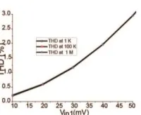
4. 3. Total Harmonic Distortion The Total
Harmonic Distortion (THD) is a measure to estimate the degree to which a system is nonlinear. Therefore the variation in THD as a function of input signal amplitude is observed. For this, a constant DC voltage of 50 mV is applied to Vin2 while a sinusoidal signal of 100 kHz is applied to Vin1 with amplitude varying. The measured THD is plotted in Figure 9.
(a) (b)
Figure 7. (a) DC characteristics of proposed multiplier (b) %
Nonlinearity curve
Figure 9. THD vs Vin1 of proposed multiplier
The similar measurements are obtained for two other input signals having frequencies 1 kHz and 1 MHz, respectively and found that for input signals < 50 mV the maximum THD remains under 3% for the proposed FQAM for all three cases.
4. 4 Noise Analysis The noise limits the minimum
signal level that a circuit can process with acceptable quality. Therefore, the effect of noise on the proposed circuit is examined through SPICE simulations. The equivalent input noise and the equivalent output noise are plotted in Figures 10(a) and 10(b), respectively with varying input frequency. For simulations, Vin1 is taken as a 100 mV AC signal whereas Vin2 is chosen as 80 mV DC value. The obseved Vinoise and Vonise are 21.75 nV/√Hz and 10.38 nV/√Hz, respectively.
5. APPLICATIONS
5. 1. Amplitude Modulator An amplitude
modulator can be designed provided the carrier and modulating signals are applied to the two inputs of an FQAM, respectively. To validate the functionality of proposed FQAM as an amplitude modulator, two sinusoids of 100 mV/100 kHz and 100 mV/10 kHz frequencies were applied at Vin1and Vin2,respectively. The input transient and corresponding spctrum are shown in Figures 11(a) and 11(b), respectively. Similarly, Figure 12(a) depicts the amplitude modulated output with its spectrum in Figure 12(b). The output frequency spectrum has two frequency components of 90 kHz and 110 kHz thereby confirming the modulation operation.
5. 2. Rectifier The rectifier can be implemented
using multiplier by taking one of the inputs as pulse type having frequency same as that of the signal which is to be rectified. To verify the workability of rectifier two inputs namely a sinusoidal signal and a square wave of 100 kHz/100 mV each were applied to the respective inputs of FQAM.
The input transient is shown in Figure 13(a) and the rectified output is presented in Figure 13(b). The simulated ripple factor curve is plotted in Figure 13 (c).
(a) (b)
Figure 10. (a) Input Noise (b) Output Noise
(a) (b)
Figure 11. (a) Input transient (b) Frequency spectrum
(a) (b)
Figure 12. (a) output transient (b) Frequency spectrum
(a) (b)
(c)
Figure 13. Time domain representation of (a) input signals (b)
output signal (c) ripple factor
534 P. Gupta and R. Pandey / IJE TRANSACTIONS A: Basics Vol. 32, No. 4, (April 2019) 528-535
6. CONCLUSION
A voltage mode FQAM based on quarter square -algebric identity employing VDBA is proposed in this paper. The circuit is suitable for integration as passive resistor may suitably be implemented using MOSFETs. The theoretical propositions have been verified through SPICE simulations using 0.18µm CMOS process parameters. The power dissipation is found low as compared to other available structures and the simulated THD is well below 3%. Applications like amplitude modulator and rectifier are predesigned using proposed structure to show its applicability and results are in total agreement with the theory.
7. REFERENCES
1. Hsiao, S.Y., and Wu, C.Y., “ A 1.2 V CMOS four-quadrant analog multiplier”,Proceedings of 1997 IEEE International Symposium on Circuits and Systems, (1997), 241–244. 2. Abuelma’atti Muhammad, M.T ., “A mode
current-controlled current -conveyor-based analogue
multiplier/divider”,International Journal of Electronics, Vol. 85, No. 1, (1998), 71–77.
3. Kaewdang, K., Fongsamut, C. and Surakampontorn, W., “A wide-band current -mode OT A-based analog multiplier-divider”,Proceedings of the 2003 IEEE International Symposium on Circuits and Systems, (2003).
4. Riewruja, V. and Rerkratn, A., “ Four-quadrant analogue multiplier using operational amplifier”, International Journal
of Electronics, Vol. 98, No. 4, (2011), 459–474.
5. Yuce, E., “Design of a Simple Current -Mode Multiplier T opology Using a Single CCCII+”, IEEE Transactions on
Instrumentation and Measurement, Vol. 57, No. 3,
(2008),631–637.
6. Chadha, U. and Arora, T ., “Four quadrant analog multiplier/divider employing single OT RA”, Proceedings of the International Conference on Communication and Computing Systems,(2016),635–639.
7. Pathak, J.K., Singh, A.K. and Senani, R. “New Multiplier/Divider Using a Single CDBA”,American Journal of
Electrical and Electronic Engineering, Vol. 2, No. 3,(2014),
98–102.
8. Keskin, A. Ü.,“A Four Quadrant Analog Multiplier Employing Single CDBA”,Analog Integrated Circuits and Signal
Processing,Vol.40, No. 1,(2004), 99–101.
9. T angsrirat, W., Pukkalanun, T ., Mongkolwai, P., and Surakampontorn, W.,“Simple current -mode analog multiplier, divider, square-rooter and squarer based on CDT As”,AEU -
International Journal of Electronics and Communications,
Vol. 65, No. 3,(2011), 198–203.
10. Hidayat, R., Dejhan, K., Moungnoul, P. and Miyanaga, Y.,“OTA-based high frequency CMOS multiplier and squaring circuit:, IEEE2008 International Symposium on Intelligent Signal Processing and Communications Systems,(2009),1-4.
11. Surakampontorn, W.,Kaewdang, K. and Fongsamut, C..,“ A Simple Current -Mode Analog Multiplier- Divider Circuit Using OT As”, 2002 International Technical Conference on Circuits, Computers and Communications, Thailand,(2002), pp. 658–61.
12. Pisutthipong, N. and Siripruchyanun, M.,“ A novel simple current -mode multiplier/divider employing only single multiple-output current controlled CTTA”. TENCON 2009 IEEE Region 10 Conference, (2009), 1–4.
13. Boonchu, B. and Surakampontorn, W.,“Power Detector Voltage-Mode CMOS Squarer/Multiplier Circuit,”International T echnical Conference on Circuits,(2002),8–11.
14. Pandey, R., Pandey, N., Sriram, B. and Paul, S. K., “ Single OT RA Based Analog Multiplier and Its Applications”,ISRN
Electronics, Vol. 2012,(2012),1–7.
15. Kaçar, F., Yeşil, A. and Noori, A., “ New CMOS realization of voltage differencing buffered amplifier and its biquad filter applications”,Radioengineering, Vol.21, No. 1,(2012), 333– 339.
16. T oumazou, C., Lidgey, F. J. and Haigh, D.,“ Analogue IC design: the current -mode approach”, IET , (1993), 1st Ed. London.
17. Biolek, D., Senani, R. and Biolková, V., “ Active Elements for Analog Signal Processing: Classification , Review , and New Proposals”, Radioengineering, Vol. 17, No. 4, (2008), 15-32 18. Herencsar, N., Cicekoglu, O., Sotner, R., Koton, J. and Vrba, K., “New resistorless tunable voltage-mode universal filter using single VDIBA”, Analog Integrated Circuits and Signal
Processing, Vol.76, No. 2,(2013), 251–260.
19. Guney, A., Alaybeyoglu, E. and Kuntman, H.,“ New CMOS realization of Z Copy Voltage Differencing Buffered Amplifier and its current -mode filter application”, IEEE 8th International Conference on Design & T echnology of Integrated Systems in Nanoscale Era, (2013), 68–71.
20. Khatib, N. and Biolek, D.,“ New voltage mode universal filter based on promising structure of Voltage Differencing Buffered Amplifier”, IEEE 23rd International Conference Radioelektronika, (2013),177–181. 25.
21. Sotner, R., Jerabek, J. and Herencsar, N.,“Voltage Differencing Buffered/Inverted Amplifiers and T heir Applications for Signal Generation”, Radioengineering,Vol. 22, No. 2, (2013), 490– 504.
22. Farshidi, E. and Keramatzadeh, A., “ A New Approach for low voltage CMOS based on current -controlled conveyors”,
International Journal of Engineering, Transactions B:
Applications, Vol. 27, No. 5, (2014),723-730.
23. Singh, S. V., T omar, R. S. and Chauhan D. S., “ A New T rans-Admittance-Mode Biquad Filter Suitable for Low Voltage Operation”, International Journal of Engineering,
Transactions B: Applications, Vol. 28, No. 12, (2015),
Voltage Differencing Buffered Amplifier based Voltage Mode Four Quadrant Analog
Multiplier and its Applications
P. Gupta, R. Pandey
Department of Electronics and Communication Engineering, Delhi Technological University, Delhi, India
P A P E R I N F O
Paper history: Received 25 July 2018
Received in revised form 20 January 2019
Accepted 07 March 2019
Keywords:
Analog Building Blocks
Voltage Differencing Buffered Amplifier Four Quadrant Analog Multiplier Quarter Square Algebraic Identity
هديكچ
( هناگراهچ گولانآ بیرض راهچ ژاتلو تلاح کی هلاقم نیا رد
FQAM
ت زا هدافتسا اب ) ( ژاتلو رفاب هدننک تیوق
VDBA
تیوه ساسا رب )
رد .تسا هدش هئارا عبرم یربج
FQAM
زا هدافتسا اب ناوت یم ار لعفنم تمواقم ،یداهنشیپ
MOSFET
ارجا عابشا هقطنم رد لماع یاه
یشیارآ ریغ رثا هلاقم نیا رد .دنک یم بسانم ماغدا یارب ار نآ نیاربانب و درک
VDBA
ارق لیلحت دروم زین یرظن یاه هرازگ .تسا هتفرگ ر
یزاس هیبش قیرط زا
SPICE
یروآ نف هرگ رد
CMOS 0.18μm
تفای یرظن ریداقم اب کیدزن قفاوت رد یزاس هیبش جیاتن و هدش دییات
ناونع هب هیذغت عبنم ژاتلو .دوش یم
±
1
V
هب یلداعت نایرج رادقم و دوش یم هبساحم 40
μA
لک کینومراه جاجوعا .دوش یم میظنت
( لخادت
T HD
زا رتمک ) 3
٪
هب هیلخت تردق لک و دوش یم هدهاشم 627
μW
داهنشیپ ییاراک .دسر یم
FQAM
همانرب ود قیرط زا زین
.دنک یم دییأت ار یرظن یاه هرازگ یزاس هیبش جیاتن .دریگ یم رارق شیامزآ دروم ،هدننک وسکی کی و هنماد روتلاودم کی ینعی ،یدربراک

![Figure 1. Block diagram of Quarter square algebraic identity [1]](https://thumb-us.123doks.com/thumbv2/123dok_us/20407.2002179/3.596.60.283.271.477/figure-block-diagram-quarter-square-algebraic-identity.webp)