Please cite this article as: S. Valiollahi and G. Ardeshir, A Simple General-purpose I-V Model for All Operating Modes of Deep Submicron MOSFETs, International Journal of Engineering (IJE), IJE TRANSACTIONS B: Applications Vol. 31, No. 2, (February 2018) 270-277
International Journal of Engineering
J o u r n a l H o m e p a g e : w w w . i j e . i rA Simple General-purpose I-V Model for All Operating Modes of Deep Submicron
MOSFETs
S. Valiollahi, G. Ardeshir*
Department of Electrical and Computer Engineering, Babol Noshirvani University of Technology, Babol, Iran
P A P E R I N F O
Paper history:
Received 04 March 2017
Received in revised form 08 June 2017 Accepted 12 October 2017
Keywords:
Deep Submicron Heuristic Optimization MOSFET Modeling nth-Power Law Model
Short Channel Effects Sub-threshold Current
A B S T R A C T
A simple general-purpose I-V model for all operating modes of deep-submicron MOSFETs is presented. Considering the most dominant short channel effects with simple equations including few parameters, a reasonable trade-off between simplicity and accuracy is established. To further improve the accuracy, model parameters are optimized over various channel widths and full ranges of operating voltages using a heuristic optimization algorithm. The obtained results demonstrate only 1.28% and 0.97% average error in IBM 0.13um CMOS technology node for NMOS and PMOS, respectively, comparing with the accurate physically-based BSIM3 model. Furthermore, the tolerance of the model accuracy against parameters variation is investigated.
doi: 10.5829/ije.2018.31.02b.10
1. INTRODUCTION1
Modeling transistors I-V characteristics is an essential of any circuit design, both for intuitive analysis on paper and also for design verification in circuit simulators. The well-known square law model fails to represent the I-V behavior of submicron MOSFETs, because of ignoring short channel effects especially the velocity saturation and mobility degradation. Therewith, many different models have been proposed for submicron regimes [1-6], which can be generally divided into two groups. a) Models [1, 2, 6] which take the accuracy as the foremost priority and sacrifice simplicity for this sake, like BSIM3 [2], i.e. suitable to be implemented in circuit simulators such as HSPICE [7]. These models focus on emulating the physical behavior of MOSFETs very accurately and continuously, hence, they are complex and incorporate a large number of parameters. b) The other group of models [3-5, 8, 9] mainly focus on fast analysis while providing a reasonable accuracy. To set a balance between simplicity and accuracy, they try to keep the complexity as low as an acceptable
*Corresponding Author’s Email: [email protected](G. Ardeshir)
[8-11], which are further discussed in section 2, tried to modify the initial nth-power law model to fit the characteristics of nanometer devices. This is quite a challenging task, since various complex phenomena influence the drain current in deep submicron devices [2]. To achieve a reasonable trade-off between simplicity and accuracy, the most dominant phenomena should be considered and approximated by simple equations and few parameters as possible. On the other hand, setting proper values to parameters is a deciding factor on the overall accuracy of the model. The parameters values should be globally optimum for full ranges of operating voltages and various channel widths. I-V equations of submicron MOSFETs are highly nonlinear, have two separate relations for linear and saturation sections, and involve at least several parameters. In such conditions, the classic gradient-base optimization methods [8] usually stuck in local extrema, and their performance highly depends on the initial guess. On the other hand, heuristic optimization methods can efficiently find the global optimum for such complex multi-variable problems without requiring carefully set initial values.
Totally, the previous modifications made on nth-power law model suffer from one or more drawbacks: not setting a reasonable trade-off between simplicity and accuracy i.e. overcomplicating the equations or adding too many extra parameters for sake of accuracy [9], designed for a special purpose like delay analysis or just applicable in digital circuits [6, 12, 13], not covering all operating modes [8, 9], and not applying a fast efficient optimization algorithm [8, 11]. Regarding the existing gaps, this paper presents an I-V model for deep submicron MOSFETs with the following main features:
A well-established simplicity-accuracy trade off The model takes into account the most dominant short channel effects through all operating modes (sub-threshold, triode, and saturation) by simple equations and few added parameters. The accuracy is further improved by optimizing the model parameters across various channel widths and full ranges of operating voltages. Furthermore, the tolerance of accuracy against each parameter variation is investigated.
General-purpose
The model is not designed for any special application. It can be used in both analog and digital circuits for any purpose where the I-V model has to be applied.
Heuristic optimization algorithm
The model parameters are optimized by a heuristic method, which can efficiently find the global optimum of such a nonlinear complex problem. Heuristic algorithms start from a random initial population and do not require a carefully selected initial point [14, 15]. They are fast and do not impose heavy computational loads on the overall
system. The applied heuristic method, named Artificial Bee Colony (ABC) [16], has only three control parameters, so it is easily configurable [17, 18].
The obtained results demonstrate only 1.28% and 0.97% error in IBM 0.13um CMOS technology node for NMOS and PMOS, respectively, comparing with the accurate physically based model of BSIM3. The rest of the paper is organized as follow. Section 2 reviews some similar models. Section 3 explains the proposed model and the optimization process. Section 4 contains the simulation results. Finally, Section 5 concludes the paper.
2. REVIEW of SOME SIMILAR MODELS
The initial nth-power law model [5] was introduced as follow.
In linear mode, VDS VDSsat
2
2
(2 DS DS )(1 ),
D Dsat DS
DSsat DSsat
V V
I I V
V V
(1)
in saturation mode, VDS VDSsat
(1 ),
D Dsat DS
I I V (2)
where
( ) ,n
e
Dsat GS t
e
W
I B V V
L
(3)
2 ,
e D
L L XL L (4)
2 ,
e D
W WXW W (5)
0 1VSB,
(6)
( ) ,m
DSsat GS t
V K V V (7)
0 ( 2 2 ).
t t F SB F
V V V (8)
DS
V , VGS, and VSB are the drain-source, gate-source and source-bulk voltages, respectively. VDSsat is the drain-source voltage at which the average carrier drift velocity saturates. We and Le are the effective channel width and length, respectively. L and W are the drawn channel length and width, respectively. X L and
channel from the bulk along the width, F is the potential difference between the electrostatic potential and the Fermi potential inside the substrate under thermal equilibrium, and Vt0 is the threshold voltage at
0 SB
V . B is a technology dependent constant, which implicitly includes mobility. is the body-effect coefficient. 0 is the channel length modulation coefficient at VSB 0. n, m, K , and 1 are
empirical constants. Therefore, at VSB 0, the six parameters of initial nth-power law are
0 0
[Vt , ,B ,K m n, , ]. As mentioned before, the initial n
th
-power law assumes mobility (included in B ) and Vt constants over all VDS and VGS which leads to a considerable inaccuracy in submicron regimes. Furthermore, the sub-threshold current is not taken into account. Hamoui [8] considered the effects of short channel length and width on Vt0 as follows:
0 (1 ),
e
t tw
e
L
V V f
W
(9)
where Vtw is the threshold voltage of wide channel MOSFETs at VSB 0 and f is an empirical factor. He modified the model with seven parameters at VSB 0 as [Vt0, , , ,f B K m n, , ]. Hamoui claimed that the DIBL effect was implicitly considered in his proposed modified model, as the threshold voltage would be optimized over the full range of VDS voltage. However, the model is not accurate enough in deep submicron regimes. Since, just optimizing the threshold voltage over VDS cannot sufficiently model the DIBL effect on
0
t
V . The mobility is not constant over all VGS. Addressing the sub-threshold current just by optimizing
tw
V is quite insufficient. Finally, a classic gradient-base optimization method would easily stick in local extrema.
The authors in [9, 11] considered the mobility degradation and hence rewrote Bas B B0. B0 is a constant and the hole and electron mobility were
empirically approximated as 2
0
/ (1 )
hole k B VDS
and
2 3/ 2 0
/ (1 ( ) )
elec k B VDS
, respectively. Where
0/ (L Ve sat)
and k B00/Le. 0 is the carrier
mobility and Vsat is the voltage at which the carrier
velocity saturates. The dominant effect of VGSon mobility degradation was not accounted [2]. The authors also applied the empirical equation C/ 1VVDS
which models the variations of with VDS[19], where
C
and V are constants. An empirical relation to
model the variation of the threshold voltage due to the DIBL effect was used as follows:
, DSsat DS t e V V V L
(10)
where
is a constant. The effects of short channel length and width were ignored while they are crucial in deep submicron devices. The authors also suggested( / ) ( / )
e W VGS GS
W W W W W V , where WW and WV GS
are constants. The authors introduced the following equation for drain current in deep inversion:
(1 ) .p
D Dsat DS
I I V (11)
while around VDSsat,the drain current was computed as follow:
(2 DS )q DS (1 ).
D Dsat DS
DSsat DSsat
V V
I I V
V V
(12)
As it is obvious, p and q added extra degrees of nonlinearity to the overall model. They considered thirteen parameters at VSB0 in their modified model as
0
[Vt ,K m n, , , C, V, , , ,k WW,WVGS, , ]p q and applied a two-stage optimization process where first the most effective parameters were selected by the genetic algorithm and then just the selected parameters were optimized by simulated annealing method i.e. a huge optimization process imposing a heavy computational load. In addition, to weak points of the model, stated above, the sub-threshold current is not considered. The author in reference [10] claimed that the proposed model to work both in moderate and inversion modes:
0 0 , , ( ) , GS t S V V N GS Th Dsat GS t GS Th S
I e V V
I
V V
I e V V
N (13)
where VTh VtNS. This modified model incorporates seven parameters at VSB 0as [Vt0,I0, , NS,K m n, , ]. The sub-threshold current, variations of Vt due to channel width and length and the DIBL effect, and the effect of channel width and length on IDsat were ignored.
Another modified nth-power law model in saturation
mode [12] was proposed as
(1 )(1 ( 1))
D Dsat m DS GS
I I V d V , where
1
( b )
m aVGS C VSB
and 1
( )n ( / n)
Dsat GS t e GS
I B V V W V .
No optimization process was applied and the parameters were extracted from BSIM4 or the same manner as [5]. This modified model incorporated ten parameters at
0 SB
degradation and variations of threshold voltage, and the sub-threshold current were ignored.
3. THE PROPOSED MODEL
Regarding the existing weak points of the similar models, discussed in details in the previous section, the proposed model takes into account the most dominant short channel effects on the drain current. These effects include the mobility degradation, threshold voltage variations due to scaling and DIBL effect, and sub-threshold current. For VGS Vt a modified version of nth-power law is proposed. However, since nth-power law is not able to model weak inversion especially in deep submicron regimes, a simple equation is added to account for the sub-threshold current. The model parameters are optimized over full ranges of VGS and
DS
V . Considering the dominant short channel effects along with parameter optimization over full ranges of operating voltages result in an accurate enough model across all operating modes. The details of the proposed model are explained as follow.
3. 1. Mobility Degradation To account for the mobility degradation effect, B is written as B B0, where B0 is a constant. The mobility is modeled, by considering the most dominant cause of its degradation i.e. VGS[2], just by adding one extra parameter (1) as follows:
0
1 . 1 VGS
(14)
3. 2. Modified Threshold Voltage The most dominant short channel effects on threshold voltage are: increasing as channel length shrinks, increasing as channel width narrows, and decreasing by VDS (DIBL), all of which are considered [8, 20], just by adding two extra parameters of
and f as follows:0 ( )(1 ),
e
t tw DS
e
L
V V V f
W
(15)
where Vtwis the threshold voltage of a long channel device at VSB 0.
3. 3. Sub-threshold Current The sub-threshold current of MOSFET is critical, especially in deep submicron regimes. It cannot be modeled just by optimizing parameters of the modified nth-power law model in sub-threshold mode, but has to be modeled separately. Some models of the sub-threshold current are complex, absolutely accurate, but not suitable for
intuitive analysis [6], and some are simple but not accurate enough because of ignoring dominant effects like exponential variations by VDS [21] or not optimizing the parameters over full ranges of operating voltages [22]. The proposed equation for the sub-threshold current, inspired from BSIM3 [2], is as follows:
0(1 ) (1 ),
DS GS t OFF sub T sub T
V V V V n V n V
Dsub DS
I I e e V
(16)
where 1nsub3, VT is the thermal voltage as KT q/ ,
OFF
V is a negative offset voltage to compensate for the threshold voltage difference in the sub-threshold mode,
is a constant proposed in this work to model the linear dependence of IDsubon VDS , and I0 is considered as follows:2
0 ,
4
e si CH
T
e B
W q N
I V
L
(17)
where
is a constant proposed here to modify I0 for deep submicron devices, and other constants are defined the same as reference [2]. The proposed modelincorporates nine parameters as
0 1 0
[Vtw, , ,f B, , ,K m n, , ] at VSB 0 in the above threshold mode, and four parameters as [ , nsub,VOFF, ] in the sub-threshold mode. Therefore, the proposed model works in all operating modes with a reasonable accuracy just by thirteen parameters.
3. 4. Optimization Process The MOSFET I-V models entail nonlinear equations involving at least several parameters, whose number grows as the channel length shrinks. Therefore, applying classic optimization methods for extracting model parameters usually results in local extrema. Heuristic optimization algorithms are efficient alternatives. The Artificial Bee Colony method is a heuristic swarm-based algorithm, proposed by Karaboga at 2005 [16] inspired from foraging behavior of honey bees. The ABC optimization algorithm best suits multi-variable continuous optimization problems, and has only three controlling parameters, hence, it is easy to configure. The following steps are repeated in the ABC algorithm until a stopping criterion is met.
Step 1: Initial Phase
A random population from the search space is formed by the following equation:
min max min
( ),
1, 2,..., and 1, 2,...,
mi i i i
X X rand X X
m SN i n
(18)
where Xmi is a solution vector, SN is the total population size or the total number of solution vectors,
min
i
X and max
i
respectively the lower and upper range of solution vector, and rand is a random number between [0,1]. The fitness of each solution is then computed.
Step 2: employed bee phase
A new solution is produced in the neighborhood of Xmi:
( ),
mi mi mi mi ki
V X X X (19)
int( ) 1.
k rand SN (20)
mi
is the a monotonic distribution of real random numbers between[ 1,1] . As can be seen from Equation (20), k is chosen randomly among {1, 2,...,SN}. The new solution replaces the previous one only if it has a better fitness.
Step 3: Onlooker Bees Phase
In this phase, a solution is selected according to its probability amount (Pm) calculated as follows by applying a selection method like Roulette Wheel:
1
( )
,
( )
m m
m SN
m m
m
fit X
P
fit X
(21)where fitm(Xm) is the fitness of solution Xm. The number of selected solution equalsSN . Then, step 2 is repeated again in the present step. All three steps iterate until a stopping criterion is met. If a solution is not improved after a predetermined number of iterations (limit), that solution is discarded and a new one is produced randomly as step 1.
The model parameters are optimized applying the following fitness function:
2 mod 1
( ) ,
. . VGS W VDS
Dmeasured D el
N N N
VGS VDS W Dmeasured
I I
E
N N N I
(22)where NV GS, NV DS, and NW are, respectively, the number of VGS, VDS, and channel widths points. IDmeasured is the accurate drain current obtained from BSIM3 model, while IDmodel is the drain current calculated by the proposed model.
4. SIMULATION RESULTS
To examine the accuracy of the proposed model, the obtained results were compared with the results of an accurate physically based method (BSIM3). To insure the efficiency of the model over different device sizes including narrow width channels, various widths between W 1Lto W 5L were considered, where
0.13
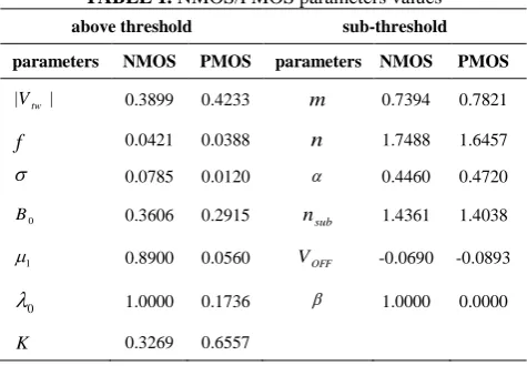
L um. The model parameters are optimized through full ranges of VGS and VDS i.e. [0,1.3 ]V . The values of model parameters for NMOS/PMOS are reported in Table 1.
TABLE 1. NMOS/PMOS parameters values
above threshold sub-threshold
parameters NMOS PMOS parameters NMOS PMOS
|Vtw | 0.3899 0.4233 m 0.7394 0.7821
f 0.0421 0.0388 n 1.7488 1.6457
0.0785 0.0120 0.4460 0.4720
0
B 0.3606 0.2915 nsub 1.4361 1.4038
1
0.8900 0.0560 VOFF -0.0690 -0.0893
0
1.0000 0.1736 1.0000 0.0000
K 0.3269 0.6557
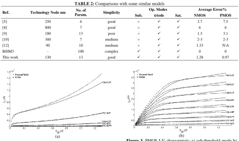
The optimization algorithm efficiently converged to the global minimum of the error function in Equation (22), over various channel widths and the full ranges of operating voltages, after about 200 iterations (as depicted in Figure 1). For both NMOS and PMOS devices, the population size was 200 and the value of limit parameter was 100. The average error was 1.28% and 0.97% for NMOS and PMOS, respectively over entire operating modes (sub-threshold, triode, and saturation). In order to demonstrate the accuracy of the proposed model, Figure 2 shows how precisely the drain current computed by the proposed model fits the exact current obtained from BSIM3 model. Since the current scaling in sub-threshold and above threshold modes are different, these two modes are depicted in separate figures for a better resolution.
(a)
(b)
Figure 1. The convergence of normalized error function for a)
The average error in the sub-threshold mode is 2.31 and 1.76% for NMOS and PMOS respectively, while in the above threshold it is 0.86 and 0.45%. As it is obvious from parameters values in Table 1, Figure 2, and Figure 3, the linear dependence of NMOS drain current on
DS
V is stronger than that of PMOS in both sub-threshold and above threshold modes.
Table 2 compares the proposed model with some other similar models and the accurate model of BSIM3 in terms of simplicity, accuracy, and generalization. As can be concluded from the table, considering the technology node, number of parameters, and equations simplicity, the proposed model establishes a robust trade-off of simplicity-accuracy and also is applicable in all operating modes for any purpose.
The number of parameters and the reported error for the proposed model are for entire operating modes. None of the reported similar models are applicable in the sub-threshold mode, while the proposed model covers all operating modes with a comparable number of parameters, simpler equations, and a better overall accuracy for both NMOS and PMOS devices.
To explain the robustness of the proposed model against parameters variations and to recognize the most sensitive parameters, the tolerance of the error function in Equation (22) is computed as follows:
_ dev opt,
opt
Error Tolerance E E
E
(23)
(a)
(b)
Figure 2. NMOS I-V characteristic a) sub-threshold mode b)
above threshold mode
TABLE 2: Comparisons with some similar models
Ref. Technology Node nm No. of
Param. Simplicity
Op. Modes Average Error%
Sub. triode Sat. NMOS PMOS
[5] 250 6 good × 3.7 7.5
[8] 800 7 good × 6 6
[9] 180 13 poor × 1.3 3.1
[10] 360 7 medium × 2-3 2-3
[12] 90 10 medium × 1.33 N/A
BSIM3 - 100 complex 0 0
This work 130 13 good 1.28 0.97
(a) (b)
Figure 3. PMOS I-V characteristic a) sub-threshold mode b)
where Edev is the deviated error from the optimum error opt
E , because of parameters variations.
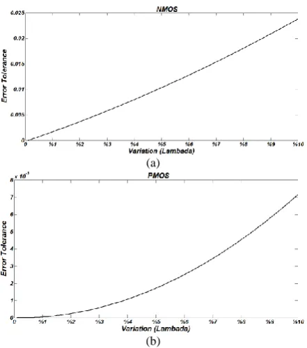
The amount of error tolerance caused by %10 variation of each parameter from its optimum value is reported in Table 3. As expected, the most sensitive parameter is the threshold voltage which is effective in all operating modes, hence its unsuitable setting leads to a considerable source of error. Most of other parameters cause less than %10 percent variations in error tolerance by changing up to %10 percent. Figure 4 shows the error tolerance caused by the variation of a sample parameter (0).
(a)
(b)
Figure 4. Error tolerance of the model with variations of 0
a) NMOS b) PMOS
TABLE 3. Error tolerance (%) with 10% variations of
parameters
Above threshold sub threshold
parameters NMOS PMOS parameters NMOS PMOS
tw
V 50.52 48.03 m 1.8 1.59
f 0.47 0.32 n 13.6 13.30
4.40 4.22
6.80 6.480
2.38 0.72
sub
n 15.90 14.30
1
0.13 0.05
OFF
V 10.21 9.55
0
B 6.32 6.14 4.00 0.00
K 3.73 3.62
5. CONCLUSIONS
A simple general-purpose I-V model for all operating modes of deep submicron MOSFETs was presented. The proposed model addressed weak points of other similar models by considering dominant short channel effects such as the mobility degradation, threshold voltage variations due to scaling and DIBL effect, and the sub-threshold current. Considering the dominant short channel effects approximated by simple equations and a reasonable number of parameters along with parameters optimization over various device sizes and full ranges of operating voltages balanced the trade-off between accuracy and simplicity robustly in all operating modes. The proposed model demonstrates only 1.28% and 0.97% average error in IBM 0.13um CMOS technology node for NMOS and PMOS, respectively, comparing with the accurate physically based model of BSIM3. Furthermore, the tolerance of accuracy against each parameter variation was investigated, which indicated the robustness of the proposed model against parameters variations.
6. REFERENCES
1. Bucher, M., Lallement, C., Enz, C.C., Théodoloz, F. and Krummenacher, F., The epfl-ekv model equations for simulation. 1998, Electronics Laboratories, Swiss Federal Institute of Technology (EPFL): Lausanne, Switzerland.
2. Cheng, Y. and Hu, C., Mosfet modeling & bsim3 user’s guide, K.A. PUBLISHERS, Editor. 2002, KLUWER ACADEMIC PUBLISHERS.
3. Qi, Z. and Stan, M.R., "Accurate back-of-the-envelope transistor model for deep sub-micron mos", in 2007 IEEE International Conference on Microelectronic Systems Education (MSE'07), San Diego, California., (2007), 75-76.
4. Sakurai, T. and Newton, A.R., "Alpha-power law mosfet model and its applications to cmos inverter delay and other formulas",
IEEE Journal of Solid-State Circuits, Vol. 25, No. 2, (1990), 584-594.
5. Sakurai, T. and Newton, A.R., "A simple mosfet model for circuit analysis", IEEE Trans. Electron Deviees, Vol. 38, No. 4, (1991), 887-894.
6. Keller, S., Harris, D.M. and Martin, A.J., "A compact transregional model for digital cmos circuits operating near threshold", IEEE Transactions on Very Large Scale Integration (VLSI) Systems, Vol. 22, No. 10, (2014), 2041-2053.
7. Hspice® reference, manual: Mosfet models. 2010.
8. Hamoui, A., "Current, delay, and power analysis of sublllicron cmos circuits", McGill University, Montréal, Department of Electrical and Computer Engineering, Master of Engineering, (1998),
9. Taherzadeh-Sani, M., Abbasian, A., Amelifard, B. and Afzali-Kusha, A., "Mos compact i-v modeling with variable accuracy based on genetic algorithm and simulated annealing", in Microelectronics, 2004. ICM 2004 Proceedings. The 16th International Conference on., (2004), 364-367.
in Proceedings of the 2005 European Conference on Circuit Theory and Design. Vol. 1, (2005), I/115-I/118.
11. Abbasian, A., Taherzadeh-Sani, M., Amelifard, B. and Afzali-Kusha, A., "Modeling of mos transistors based on genetic algorithm and simulated annealing", in 2005 IEEE International Symposium on Circuits and Systems., (2005), 6218-6221 Vol. 6216.
12. Singh, A.K., Samanta, J. and Bhaumik, J., "Modified i-v model for delay analysis of udsm cmos circuits", in 2012 International Conference on Communications, Devices and Intelligent Systems (CODIS), (2012), 357-360.
13. Consoli, E., Giustolisi, G. and Palumbo, G., "An accurate ultra-compact i-v model for nanometer mos transistors with applications on digital circuits", IEEE Transactions on Circuits and Systems-I: Regular Papers, Vol. 59, No. 1, (2012), 159-169.
14. Yegane, B.Y., Kamalabadi, I.N. and Khanlarzade, N., "Critical path method for flexible job shop scheduling problem with preemption", International Journal of Engineering (IJE) TRANSACTIONS B: Applications, Vol. 30, No. 2, (2017), 261-269.
15. Samoei, P., Khodakarami, V. and Fattahi, P., "Mixed-model assembly line balancing with considering reliability",
International Journal of Engineering (IJE) Transactions C: Aspects, Vol. 30, No. 3, (2017), 411-423.
16. Karaboga, N., An idea based on honey bee swarm for numerical optimization. 2005, Erciyes University, Engineering Faculty, Computer Engineering Department: Turkey.
17. S. Valiollahi, R.G., A. Ebrahimzadeh, "A q-learning based continuous tuning of fuzzy wall tracking without exploration",
International Journal of Engineering (IJE) Transactions A: Basics, Vol. 25, No. 4, (2012), 355-366.
18. Z. Guo, S.W., X. Yue, D. Jiang, K. Li, "Elite opposition-based artificial bee colony algorithm for global optimization",
International Journal of Engineering (IJE) Transactions C: Aspects, Vol. 28, No. 9, (2015), 1268-1275.
19. Tsividis, Y., "Operation and modeling of the mos transistor., McGraw-Hill, (1999).
20. Langevelde, R.v. and Klaassen, F.M., "Accurate drain conductance modeling for distortion analysis in mosfets", in IEDM1997 Tech. Digest., (1997), 313-316.
21. Comer, D.J. and Comer, D.T., "Operation of analog mos circuits in the weak or moderate inversion region", IEEE Transactions on Education, Vol. 47, No. 4, (2004), 430-435.
22. Gupta, K.A., Anvekar, D.K. and V, V., "Modeling of short channel mosfet devices and analysis of design aspects for power optimisation", International Journal of Modeling and Optimization, Vol. 3, No. 3, (2013), 266-271.
A Simple General-purpose I-V Model for All Operating Modes of Deep Submicron
MOSFETs
S. Valiollahi, G. Ardeshir
Department of Electrical and Computer Engineering, Babol Noshirvani University of Technology, Babol, Iran
P A P E R I N F O
Paper history:
Received 04 March 2017
Received in revised form 08 June 2017 Accepted 12 October 2017
Keywords:
Deep Submicron Heuristic Optimization MOSFET Modeling nth-Power Law Model
Short Channel Effects Sub-threshold Current
ديكچ ه
نایرج لدم -هداس هروظنم همه ژاتلو یم هئارا قیمع نورکیمریز تفسام یاهروتسیزنارت یراک یحاون یمامت یارب یا
اب .دوش
هحلاصم ،رتماراپ یمک دادعت لماش هداس یتلاداعم بلاق رد هاتوک لاناک تارثا نیرترثوم نتفرگ رظن رد یقطنم یا
یگداس نایم
ضرع یور لدم یاهرتماراپ ،تقد رتشیب دوبهب تهج .تسا هتفای تقد و هدودحم و فلتخم لاناک یاه
یاهژاتلو لماک یاه
هنیهب متیروگلا زا هدافتسا اب یراک هدش هنیهب یراکتبا یزاس
طسوتم یاطخ اهنت هدمآ تسد هب جیاتن .دنا 1.28
و % 0.97 رد ار %
یژولونکت
IBM 0.13um CMOS
یارب بیترت هب
NMOS
و
PMOS
قیقد یکیزیف لدم اب هسیاقم رد ،
BSIM3
ناشن
یم هدش یسررب رتماراپ تارییغت هب تبسن لدم تقد فارحنا ،هولاع هب .دنهد .تسا