Abstract—In the manufacturing process of Integrated Circuit (IC), defects existing in real layout are inevitable. Defects cause circuit fault, which reduces the yield and increases the IC cost. Reducing the Critical Area (CA) can lower the occurrence of circuit fault. In this paper, a novel model of Open Critical Area (OCA) are proposed. Firstly, according to the net matrix and the morphological theory, the edge of nets is extracted. Secondly, the defect replications are operated on all horizontal lines and vertical lines of the edge of nets. Then, we extract the OCA extraction on nets by reducing replication times and increasing the moving distance of defects. Finally, in order to further reduce the extraction time of OCA, the new model is implemented on Hadoop. Compared with the existing model based on the net flow-axis, the experimental results on synthesized OpenSparc circuit and three nodes of the cluster on Hadoop show that the proposed model is more efficient without accuracy loss.
Index Terms—open critical area, defects, Hadoop
I. INTRODUCTION
With the boom in nanoscale IC [1]-[3], it is difficult to acquire the desired yield by making use of the IC design rules when designing layouts [4]-[9]. For the sake of determining the yield loss mainly caused by defects in the manufacturing process [10], [11], experts proposed the definition and extraction algorithm of CA [12]-[18]. CA is the area of a layout at which the occurrence of a defect would result in functional failure. If the area where the occurrence of a defect would result in an open failure, it is called OCA. The yield can be raised successfully by reducing CA of layouts, thereby reducing IC cost [19], [20]. Concern for the accuracy and extraction efficiency of CA is at the core of yield improvement [21].
For the extraction of CA, the model proposed by Wang et al. is relatively precise because it is based on the net flow-axis [22]. It can extract CA of different shapes nets with higher precision, but with low efficiency and high time complexity. Contrast to the former, the model proposed by Wang and Wu is more efficient, which lowers the time complexity and reduces the extraction time of short CA [23]. But it does not put forward OCA model and rapid extraction algorithm, which is the key factor restricting the layout optimization and sensitivity calculation. In order to reduce extraction time of OCA
Manuscript received May 15, 2019; revised November 25, 2015.
and receive a high precision, this paper proposes a new model of OCA. This model is first applied to the edge of arbitrary nets. In new model, CA extraction of arbitrary nets is optimized. Replication times of defects on arbitrary nets is reduced owing to the reason that the defect centroid is moved a defect’s feature size rather than a grid unit when continuing to copy next defect. Moreover, because a defect is copied partially on rectangle nets, the number of points of one replication operation is also decreased. Since implemented on Hadoop, novel model further improves OCA extraction speed.
II. NOVEL MODEL OF OCA
OCA of layouts is caused by defects. In the novel model, the layout and defect can both be converted to a two-dimensional matrix. If the point is covered by nets or defect, the matrix value of this point is 1.
A. Novel Modeling of OCA Based on Defect Characteristics
For a single net N i, j
with row range and columnrange, whose OCA can be obtained by expanding the boundary of this net. For a random defect D X ,Y
C C
,suppose the characteristic size of a defect is D u D u1 2 ,
and the centroid is
X ,YC C
. u is the size of a grid oncircuit layout. The OCA composed of the centroid of the defect on the net is as shown in formula (1)–(3).
1
1
H i H i
V j V j
numi
O C C R H H
i H i j y
numj
R V V i x
j j V
A X ,Y ,N D i , j
D i , j
(1)
1 2 1
i min min min max
H x ,x D ,x D ,...,x (2)
2 2 2
i min min min max
V y , y D , y D ,..., y (3)
In formula (1), AO
X ,Y ,NC C
is a two-dimensionalmatrix, whose size is same as the layout. The area of
O C C
A X ,Y ,N in which matrix value exceeds 1 is defined as OCA. numi is the number of horizontal lines
Novel
M
odel of OCA in IC and Its
Implementation on Hadoop
Shulei Wei and Junping Wang
©2019 Int. J. Electron. Electr. Eng. 75 in boundary of this net.
numj
is the number of verticallines in boundary of this net. Hi represents the numerical range of the x-axis direction crossed by the ith horizontal line. yi represents the value of the y-axis direction
occupied by the ith horizontal line. Vj represents the
numerical range of the y-axis direction crossed by the jth vertical line. xj represents the value of the x-axis
direction occupied by the jth vertical line.
B. Algorithm Steps of Novel Model
In order to improve the feasibility of novel model given in previous section, corresponding algorithm steps are proposed. The layout and defect can be transformed into a two-dimensional matrix. The conversion rule of layout is defined as follows, if the net covers the point
i, j , then the value on this point in matrix equals 1, otherwise 0. The transformation rule of the defect in matrix is similar to the above conversion, if the defect overlap with the point
i, j , then the value on this pointin matrix equals 1, otherwise 0.
Algorithm Steps. Algorithm steps to extract OCA according to novel model
Step 1 Obtain binary image of a layout and save it in a matrix imgN1N2 and create a matrix resultN1N2 whose value of every point are 0.
Step 2 Extract the characteristics and centroid of the defect, and save the defect in a matrix
1 2
D D
D .
Step 3 Split every net in layouts according to connectivity, label a single net n which is a positive number smaller than num,num is the number of nets, and initialize n with integer 1.
Step 4 Extract the boundary of the net. Moreover, obtain horizontal lines and vertical lines in the boundary.
Step 5 Get the numerical range of the x-axis direction
xmin,xmax
and the value of the y-axis directiony
of thehorizontal line. Initialize the point
R Cm, n
of net nwith
xmin, y
.Step 6 CopyD R
m,Cn
, and append the replicationresult in corresponding points of re sultN1N2 . If
max
m
R x , then RmRmD1 and return to Step 6, otherwise jump to Step 7.
Step 7 If all horizontal lines have been processed, return to Step 5, otherwise jump to Step 8.
Step 8 Get the numerical range of the y-axis direction
ymin, ymax
and the value of the x-axis directionx
of thevertical line. Initialize the point
R Cm, n
of netn
with
x, ymin
.Step 9 Copy D R
m,Cn
, and append the replicationresult in corresponding points of re sultN1N2 . If
max
n
C y , then CnCnD2 and return to Step 9, otherwise jump to Step 10.
Step 10 If all vertical lines have been processed, return to Step 8, otherwise jump to Step 11.
Step 11 Letn=n+1, if nnum, return to Step 4, otherwise jump to Step 12.
Step 12 Compute the area of the domain where the matrix value exceeds 1 in re sultN1N2.
The explanation of the algorithm above is shown as follows. Steps 1–3 can determine layout matrix, defect matrix and the number of nets. Step 4 obtains horizontal lines and vertical lines in the boundary of nets. Defect replication of each horizontal line is realized in Step 5-7.Similarly, defect replication of each vertical line is realized in Step 8-11. The step 12 completes the extraction operation for all nets. The step 14 calculates the value of OCA.
C. Performance Analysis of Novel Model
In this paper, we analyze mainly the time complexity of the novel model. The executive time of the model on a net of rn rows and cn columns mainly depends on the defect copy operation of certain options. Because this model is realized in the boundary of a net and the defect centroid is moved a defect’s feature size rather than a grid
unit, so times of copy operation on a net are
1
2 rn 1
D
or
2
2 cn 1
D
. 1
2 rn 1
D
is times of copy operation on
the horizontal net, and
2
2 cn 1
D
is times of copy
operationon thehorizontalnet. Furthermore, the number of points of a copy operation on a single net is D1D2. Let constant C be the time of one assignment operation, so the time of replication operation on a net is
1 2
1
2 2
n r
C D D
D
or 2 1 2
2 2
n c
C D D
D
.
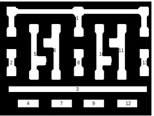
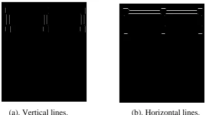
In order to understand better the advantage of new model in the time complexity, we analyze each net of a layout named SRAM in Fig. 1. Aimed to a single net labeled integer from 1 to 13, for the net 1, its components–vertical and horizontal lines are extracted in Fig. 2. Moreover, times of the defect copied is analyzed in Fig. 3. In the graph above, compared with the two model from Reference [11] and Reference [22] severally, the new model proposed in this paper is superior to them whether times of the defect copied.
1
2
3 4
5 6
7 8
9 10 11
12 13
(a). Vertical lines. (b). Horizontal lines.
Figure 2. Components the net 1–vertical and horizontal lines.
Figure 3. Times of the defect copied on each net.
III. IMPLEMENTATION OF NOVEL MODEL
To verify suitability of the new model, every layout layer of 43-active from synthesized OpenSparc circuit is tested under different defect sizes. There are the 7 group layouts in these layout layers, and each group has different number of nets.Nets represents the number of nets on the layout layer. The feature size of the defect is taken as 18u18u,20u20u and 25u25u respectively. Theu2is the unit of the OCA, and u is the size of a grid on circuit layout. The unit of time is s (second).
A. Implementation of New Algorithm
The proposed model in this paper and the existing model in [22] are implemented on the same computer. Hardware configurations of the computer are: Intel(R) Pentium (R) CPU G 645 @ 2.90 GHz and 4 GB’s memory physical address extension. Experiment results is shown as Table I, Table II and Table III. Among which, the column AO represents the OCA applying the existing
model in Reference [22], and AN represents the OCA
applying the proposed model in this paper. Similarly, TO
and TNrepresent the extraction time applying the existing model in Reference [22] and the proposed model in this paper respectively.
From Table I, Table II and Table III, AN is equal to
O
A . However, TN is obviously less than TO. It is proved that the proposed model in this paper significantly improves the extraction efficiency of OCA under the condition of guaranteed accuracy. This characteristic is advantageous to the development of IC.
TABLE I. THE SIZE OF DEFECT IS 18u18u
Layout Nets (10 ) / u6 2
O
A (10 ) / u6 2
N
A (10 ) / s4
O
T (10 ) / s4
N
T
1 6577 4.404 4.404 0.920 0.239
2 4990 4.595 4.595 0.746 0.160
3 3696 1.342 1.342 0.401 0.093
4 30,824 31.563 31.563 5.157 0.829
5 23,505 23.297 23.297 3.755 0.611
6 6216 6.951 6.951 0.868 0.189
7 12,816 9.538 9.538 1.818 0.376
TABLE II. THE SIZE OF DEFECT IS 20u20u
Layout Nets 6 2
(10 ) / u O
A 6 2 (10 ) / u N
A 4 (10 ) / s O
T 4 (10 ) / s N
T
1 6577 11.549 11.549 0.925 0.259
2 4990 7.716 7.716 0.850 0.169
3 3696 2.243 2.243 0.464 0.097
4 30,824 65.831 65.831 5.328 1.249
5 23,505 38.385 38.385 3.830 0.917
6 6216 11.153 11.153 0.906 0.195
7 12,816 15.654 15.654 1.899 0.378
TABLE III. THE SIZE OF DEFECT IS 25u25u
Layout Nets (10 ) / u6 2
O
A (10 ) / u6 2
N
A (10 ) / s4
O
T (10 ) / s4
N
T
1 6577 17.236 17.236 0.950 0.259
2 4990 13.974 13.974 0.954 0.196
3 3696 5.552 5.552 0.464 0.097
4 30,824 99.013 99.013 5.744 1.656
5 23,505 69.848 69.848 5.208 1.211
6 6216 20.001 20.001 0.961 0.196
7 12,816 26.396 26.396 2.124 0.411
B. Implementation on Hadoop
Nowadays, IC scale becomes increasing larger, so it is not enough to only improve the efficiency of the model. Hadoop is a software framework allowing for the distributed processing of large amounts of data, whose characteristics are high reliability, efficiency, expansibility and high fault tolerance. So, we implement the model on Hadoop [24]. In order to test the efficiency of new model proposed in this paper, this model and the existing model in Reference [22] are implemented on the same Hadoop system. With Hadoop system built by three nodes, the configuration information and IP address of each node in the cluster are shown in Table IV. In addition, the operating system of each node is same, which is equipped with CentOS 6.3.
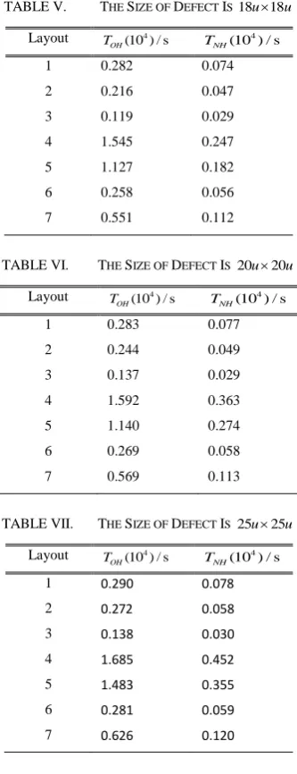
TABLE IV. THE SIZE OF DEFECT IS 18u18u
configure Master. Hadoop Slave1.Hadoop Slave2.Hadoop IP
address 192.168.1.219 192.168.1.220 192.168.1.221
CPU Pentium(R) D CPU 2.80GHz
Pentium(R) Dual-CoreCPU
E5800 @ 3.20GHz
Pentium(R) Dual-CoreCPU
E5800 @ 3.20GHz Physical
memory 2G 2G 2G
Hadoop
TABLE V. THE SIZE OF DEFECT IS 18u18u
Layout 4
(10 ) / s
OH
T 4
(10 ) / s
NH
T
1 0.282 0.074
2 0.216 0.047
3 0.119 0.029
4 1.545 0.247
5 1.127 0.182
6 0.258 0.056
7 0.551 0.112
TABLE VI. THE SIZE OF DEFECT IS 20u20u
Layout 4
(10 ) / s
OH
T 4
(10 ) / s
NH
T
1 0.283 0.077
2 0.244 0.049
3 0.137 0.029
4 1.592 0.363
5 1.140 0.274
6 0.269 0.058
7 0.569 0.113
TABLE VII. THE SIZE OF DEFECT IS 25u25u
Layout (10 ) / s4
OH
T (10 ) / s4
NH
T
1 0.290 0.078
2 0.272 0.058
3 0.138 0.030
4 1.685 0.452
5 1.483 0.355
6 0.281 0.059
7 0.626 0.120
Experiment results is shown as Table V, Table VI and Table VII. With Hadoop, the column TOH represents the extraction time applying the existing model in Reference [22], and TNH represents the extraction time applying proposed model in this paper.
From Table V, Table VI and Table VII, TNH is
obviously less than TOH, which verifies that the proposed model is also feasible for Hadoop. Moreover, the extraction efficiency of OCA is further improved.
IV. CONCLUSION
In this paper, a new model of OCA is proposed. It can improve the extraction efficiency of OCA. Furthermore, implemented on Hadoop, the novel model further raises the OCA extraction speed. On the real layout, the experimental results verify the high efficiency and accuracy of new model. The new model proposed in this paper can be widely used in IC because of its advantages. Moreover, this model can offer the valuable advice for layout optimization and yield evaluation, and then the cost of IC fabrication can be reduced.
ACKNOWLEDGMENT
This work was supported by the National Natural Science Foundation of China under Grant 61872433.
REFERENCES
[1] X. Gao and L. Macchiarlo, “Track routing optimizing timing and yield,” presented at the 16th Asia and South Pacific Design Automation Conference, Yokohama, Japan, January 15-28, 2011. [2] W. Khalil, et al., “Toward millimeter-wave DACs: Challenges and
opportunities,” presented at IEEE Compound Semiconductor Integrated Circuit Symposium (CSICS), La Jolla, CA, USA, October 14-17, 2012.
[3] J. J. Zhu, et al., “Scratch-concerned yield algorithm ing for IC manufacturing involved with a chemical mechanical polishing process,” Journal of Zhejiang University SCIENCE C, vol. 13, no. 5, pp. 376-384, Jan. 2012.
[4] P. Vijayakumar, V. B. Suresh, and S. Kundu, “Lithography aware critical area estimation and yield analysis,” presented at IEEE International Test Conference, Anaheim, CA, USA, Sept. 20-22, 2011.
[5] M. Cho, et al., “Track routing and optimization for yield,” IEEE Transactions on Computer-Aided Design of Integrated Circuits and Systems, vol. 27, no. 5, pp. 872-882, April 2008.
[6] P. J. Ma, Y. Hao, and H. X. Liu, “Analysis and simulation of effect of pinhole defects on integrated circuits functional yield,”
Chinese Journal of Semiconductors, vol. 21, no. 1, pp. 102-106, 2001.
[7] H. Walker and S. W. Director, “VLASIC: A catastrophic fault yield simulator for integrated circuits,” IEEE Transactions on Computer-Aided Design of Integrated Circuits and Systems, vol. 5, no. 4, pp. 541-556, Oct. 1986.
[8] J. P. Wang and Y. Hao, “Yield algorithm of IC based on distribution of defect shapes,” Chinese Journal of Semiconductors, vol. 26, no. 8, pp. 1054-1058, May 2005.
[9] C. Chiang and J. Kawa, “Three DFM challenges: Random defects, thickness variation, and printability variation,” presented at IEEE Asia Pacific Conference on Circuits and Systems, Singapore, Singapore, Dec. 4-7, 2006.
[10] T. X. Gong and Y. J. Wang, “Mass defect effect in the gravitational field,” Chinese Physics, vol. 14, no. 1, pp. 45-48, 2005.
[11] J. P. Wang and Y. Hao, “Critical area computation for real defects and arbitrary conductor shapes,” Chinese Physics, vol. 15, no. 7, pp. 1621-1630, 2006.
[12] S. K. Dey, et al., “Layout pattern analysis using the Voronoi diagram of line segments,” Journal of Micro-Nanolithography MEMS and MOEMS, vol. 15, no. 1, pp. 1621-1631, Feb. 2016. [13] J. P. Wang and Y. Hao, “Efficient WCA algorithm for 65–90 nm
processes,” Acta Physica Sinica, vol. 58, no. 6, pp. 4267-4273, Oct. 2009.
[14] G. A. Allan and A. J. Walton, “Critical area extraction for soft fault estimation,” IEEE Transactions on Semiconductor Manufacturing, vol. 11, no. 1, pp. 146-154, Feb. 1998.
[15] W. A. Pleskacz, C. H. Ouyang, and W. Maly, “A DRC-based algorithm for extraction of critical areas for opens in large VLSI circuits,” IEEE Transactions on Computer-Aided Design of Integrated Circuits and Systems, vol. 18, no. 2, pp. 151-162, Feb. 1999.
[16] S. T. Zachariah and S. Chakravarty, “A scalable and efficient methodology to extract two node bridges from large industrial circuits,” presented at Proceedings International Test Conference, Oct. 3-5, 2000.
[17] X. L. Sun, Y. Hao, and G. X. Song, “The study of multifractal characterization of IC defect outline,” Journal of Electronics and Information Technology, vol. 29, no. 2, pp. 496-498, Feb. 2005. [18] J. J. Zhu, et al., “An improved shape shifting method of Critical
area extraction,” Journal of Semiconductors, vol. 35, no. 2, 2014. [19] D. Müller, “Optimizing yield in global routing,” presented at 2006
IEEE/ACM International Conference on Computer Aided Design, San Jose, CA, USA, Nov. 5-9, 2006.
[20] S. Lee, W. Kang, and H. Shin, “Detection and elimination of a yield-critical non-visual residue defect,” Solid State Technology, vol. 56, no. 4, 2013.
[21] A. Canelas, et al., “Efficient yield optimization method using a variable K-Means algorithm for analog IC sizing,” presented at Design, Automation & Test in Europe Conference & Exhibition (DATE), Lausanne, Switzerland, March 27-31, 2017.
[22] L. Wang, et al., “Open critical area algorithm and extraction algorithm based on the net flow-axis,” Chinese Physics B, vol. 22, no. 12, pp. 531-536, 2013.
[23] J. P. Wang, Y. Wu, and T. W. Zhao, “Short critical area model and extraction algorithm based on defect characteristics in integrated circuits,” Analog Integrated Circuits and Signal Processing, vol. 91, no. 1, pp. 83-91, Aug. 2017.
[24] M. Sogodekar, S. Pandey, I. Tupkari, and A. Manekar, “Big data analytics: Hadoop and tools,” in Proc. Bombay Section Symposium, Baramati, India, Dec. 21-22, 2017, pp. 1-6.
Jun-Ping Wang received the B.S. degree in
computer engineering, the M.S. degree in pattern recognition and artificial intelligence, and the Ph.D. degree in microelectronics from Xidian University, Xi’an, China, in 1986, 1992, and 2005, respectively.
She is currently a Professor of Telecommunications Engineering with Xidian University. Three national patents have been declared. The number of published papers in important journals is more than 40, in which nearly 30 articles have
been indexed by SCI, EI, and ISTP. Her current research interests include physical design for VLSI circuits, design for manufacturability, multimedia communication, and image/video processing.
Dr. Wang is a member of the Shaanxi Communication Association and the China Communication Association. She holds research projects that received the second prize of Shaanxi province scientific and technological progress. She has received the Eastern Research Grants of Xidian University, and a prize for excellent papers of the 13th National Youth Communication Meeting. She is a Reviewer of international academic conference of the IEEE Computational Intelligence Society in 2006, the Section Chair of international academic conference of the IEEE International Conference on Anti-Counterfeiting, Security and Identification in 2008, and a Reviewer of the Journal of Xidian University, the Journal of Systems Engineering and Electronics, and the Journal of Communications.
Shu-Lei Wei received the B.S. degree in
communication engineering from Yan Tai University, Yantai, China, in 2016, and master’s degree from the School of Telecommunications Engineering, Xidain University, Xi’an, China.