Chemistry Publications
Chemistry
2005
Sensing Dipole Fields at Atomic Steps with
Combined Scanning Tunneling and Force
Microscopy
Jeong Young Park
Lawrence Berkeley National Laboratory
G. M. Sacha
Lawrence Berkeley National Laboratory
M. Enachescu
Lawrence Berkeley National Laboratory
D. F. Ogletree
Lawrence Berkeley National Laboratory
R. A. Ribeiro
Iowa State UniversitySee next page for additional authors
Follow this and additional works at:
http://lib.dr.iastate.edu/chem_pubs
Part of the
Biological and Chemical Physics Commons
,
Materials Science and Engineering
Commons
, and the
Physical Chemistry Commons
The complete bibliographic information for this item can be found at
http://lib.dr.iastate.edu/
chem_pubs/48
. For information on how to cite this item, please visit
http://lib.dr.iastate.edu/
howtocite.html
.
This Article is brought to you for free and open access by the Chemistry at Iowa State University Digital Repository. It has been accepted for inclusion in Chemistry Publications by an authorized administrator of Iowa State University Digital Repository. For more information, please contact
Tunneling and Force Microscopy
Abstract
The electric field of dipoles localized at the atomic steps of metal surfaces due to the Smoluchowski effect were measured from the electrostatic force exerted on the biased tip of a scanning tunneling microscope. By varying the tip-sample bias the contribution of the step dipole was separated from changes in the force due to van der Waals and polarization forces. Combined with electrostatic calculations, the method was used to determine the local dipole moment in steps of different heights on Au(111) and on the twofold surface of an Al-Ni-Co decagonal quasicrystal.
Keywords
Ames Laboratory, Materials Science and Engineering, Physics and Astronomy
Disciplines
Biological and Chemical Physics | Materials Science and Engineering | Physical Chemistry
Comments
This article is fromPhysical Review Letters95, no. 13 (2005): 136802, doi:10.1103/PhysRevLett.95.136802.
Authors
Jeong Young Park, G. M. Sacha, M. Enachescu, D. F. Ogletree, R. A. Ribeiro, Paul C. Canfield, Cynthia J. Jenks, Patricia A. Thiel, J. J. Sáenz, and M. Salmeron
Sensing Dipole Fields at Atomic Steps with Combined Scanning Tunneling and Force Microscopy
Jeong Young Park,1G. M. Sacha,1M. Enachescu,1D. F. Ogletree,1R. A. Ribeiro,2P. C. Canfield,2C. J. Jenks,3 P. A. Thiel,3J. J. Sa´enz,4and M. Salmeron1,*
1Materials Sciences Division, Lawrence Berkeley National Laboratory, University of California, Berkeley, California 94720, USA
2Ames Laboratory and Department of Physics and Astronomy, Iowa State University, Ames, Iowa 50011, USA
3Ames Laboratory, and Departments of Chemistry, and of Materials Science and Engineering, Iowa State University,
Ames, Iowa 50011, USA
4Departamento de Fı´sica de la Materia Condensada, Universidad Auto´noma de Madrid, 28049-Madrid, Spain
(Received 17 May 2005; published 21 September 2005)
The electric field of dipoles localized at the atomic steps of metal surfaces due to the Smoluchowski effect were measured from the electrostatic force exerted on the biased tip of a scanning tunneling microscope. By varying the tip-sample bias the contribution of the step dipole was separated from changes in the force due to van der Waals and polarization forces. Combined with electrostatic calculations, the method was used to determine the local dipole moment in steps of different heights on Au(111) and on the twofold surface of an Al-Ni-Co decagonal quasicrystal.
DOI:10.1103/PhysRevLett.95.136802 PACS numbers: 73.30.+y, 68.37.Ef, 68.37.Ps, 71.23.Ft
The different electronic structure of the atoms at steps and terraces of metal surfaces is thought to be responsible for their different (often-enhanced) chemical reactivity. Dipole moments are postulated to exist localized at the steps due to incomplete screening of the positive ion cores by conduction electrons, because the spatial variation of the charge density is limited by the Fermi wavelength. This is known as the Smoluchowski effect [1]. Indirect support for this assumption is provided by work-function (’) mea-surements. Besocke and Wagner found a decrease in ’ proportional to the step density on Au(111) [2] and used this to estimate the average value of the step dipole. Similar results have been reported for Pt(111) and W(110) [3,4]. Calculations using the jellium model [5] predict that the localized step dipole increases with step height and screen-ing length. Electronic structure calculations for the (111) and (100) microfacet steps on Al(111) produced very small dipole moments [6], indicating that the Smoluchowski effect alone is insufficient to fully describe the electronic structure of steps. It is therefore important that the presence and the magnitude of local dipole moments at steps be measured experimentally.
Scanning probe microscopy can be used to investigate the electronic structure of steps. Marchonet al.observed a reduction in the tunneling barrier at surface steps on sulfur-covered Re(0001) [7] using scanning tunneling micros-copy (STM). Later Jia et al.used this effect to calculate the step dipole for Au(111) and Cu(111) [8]. Arai and Tomitori investigated step contrast as a function of tip bias on Si(111) (77) using dynamic atomic force mi-croscopy (D-AFM) [9] and suggested that step dipoles could explain their observations. In contrast, Guggisberg et al. investigated the same system using STM feedback combined with D-AFM force detection and concluded that the step dipole moments inSi111-77were negligible [10]. They attributed the D-AFM contrast effects to
changes in the van der Waals and electrostatic polarization forces, which are reduced above and increased below the step edges relative to the flat terrace.
In this Letter we report measurements of the strength of the fields produced by step dipoles by direct measurement of the electrostatic force they produce on biased tips. We use a combined STM-AFM system [11] with cantilevers that are made conductive by a 30 nm coating of W2C [12]. Relatively stiff cantilevers of 48 or 88 N=m were used to avoid jump-to-contact instabilities close to the surface. Attractive forces cause the cantilevers to bend toward the surface during imaging, as illustrated in Fig. 1(a). Scanning is done at constant current as in stan-dard STM mode, while forces are measured simulta-neously from the cantilever deflection [13].
The force acting on the tip is the sum of van der Waals and electrostatic contributions. The former is independent of the applied bias. The electrostatic contributions are additive and can be written as [14]
FfD=RV2gD=RPVhD=RP2; (1)
whereDis the tip-surface distance,Rthe tip radius, andf, g, andhare functions of the tip and sample geometry.Pis the dipole moment, and V is the electrostatic potential difference between tip and sample. The first term in [1] represents the attractive force from polarization (i.e., im-age charges) induced by the applied voltim-age. The second term is due to surface dipolesPinteracting with the biased tip, and is proportional to the bias. The last term is the force between the dipole P and its image on the tip. Of these contributions only the second term is linear with applied voltage, and provides an easy way to determine the net effect of the dipole field.
The measurements were carried out in ultrahigh vacuum with an optical deflection AFM [15]. Several samples were used, including Pt(111), Au(111), and the twofold surface PRL95,136802 (2005) P H Y S I C A L R E V I E W L E T T E R S 23 SEPTEMBER 2005week ending
of aAl74Ni10Co16decagonal quasicrystal prepared by cut-ting the crystal parallel to the tenfold axis. The growth and characterization of the Al-Ni-Co quasicrystal are outlined in detail elsewhere [16]. Because of the aperiodic nature of the atomic layering in the latter sample, steps of various heights were readily obtained on a single surface. The Pt single crystal and the quasicrystal [17] samples were sput-tered and annealed in UHV. The Au sample was in the form of a thin film on glass, prepared in air by flame annealing and transferred to vacuum without further treatment. An average tip radius of 30 –70 nm was determined by scan-ning electron microscopy imaging.
Figures 1(b) and 1(d) shows the STM topography and force image of Pt(111) obtained simultaneously for a tip bias of0:2 V. Figure 1(c) is a height and force profiles across the line in 1(b). The force, which is always attrac-tive, increases by1:5 nN as the tip approaches the bot-tom of the step and decreases by 4 nN after climbing over the step. When the attractive force increases, the STM current feedback loop retracts the base of the cantilever to keep the tunnel current, and hence the tip-sample distance, constant. The reduction of attractive force in the upper side of the steps is due to the reduction in the van der Waals and polarization part of the force (image charges), since in that position half of the surface (the lower terrace) is farther away from the tip. This is consistent with the results of Guggisberg [10]. By itself this result does not prove the existence of localized dipoles at the steps. For that we need to examine the changes in the force due to applied bias.
Earlier studies of decagonal Al-Ni-Co quasicrystal sur-faces [18] indicate that the bulk structure consists of pairs
of layers with fivefold quasiperiodic structure stacked along the tenfold direction with a periodicity of 0.4 nm. In our twofold surface this produces rows of atoms ar-ranged periodically. The rows are separated by distances varying in an aperiodic manner and are parallel to the step edges. Most steps have heights of 0.5, 0.8, and 1.3 nm, although a few are observed also with 0.2 nm. The ratios of these heights follow the golden mean (1:618), characteristic of their quasiperiodic nature. Figure 2(a) shows a topographic profile perpendicular to the tenfold axis, along with corresponding force profiles acquired at 1:2and 1:2 V tip bias (at 100 pA tunneling current). Figure 2(b) shows similar topographic and force profiles across single- and double-height steps on Au(111) at 3
and3 Vtip bias. As in the Pt case, there is a reduction of the attractive force when the tip crosses over the steps (upward peaks in the force profile). While this reduction is present for both and biases, there is a noticeable difference between the two. The difference between forces at opposite biases eliminates all contributions except that from the second term in Eq. (1), which is purely due to the step dipole. We can immediately conclude that the positive end of the step dipole points up, consistent with a smaller attractive force at the positive tip bias.
Approach curves (force and current versus distance at fixed bias) were used to determine an STM tip-sample distance of 0:50:1 nm during tunneling as shown in
0 20 40 60
x (nm) Fn ( u ni t : 20nN ) -10 -5 0 5 h ei gh t (n m )
-100 -50 0 50 100 x(nm) F n (u n it : 5 n N ) -5 -4 -3 -2 -1 0 1 he ig h t (n m )
(a)
(b)
8Å 8Å 2Å 13Å
8Å
5Å
Vt=+1.2V
Vt=-1.2V
Vt=+3V
Vt=-3V
2.5Å 5Å 5Å attractive attractive repulsive repulsive
0 20 40 60
x (nm) Fn ( u ni t : 20nN ) -10 -5 0 5 h ei gh t (n m )
-100 -50 0 50 100 x(nm) F n (u n it : 5 n N ) -5 -4 -3 -2 -1 0 1 he ig h t (n m )
(a)
(b)
8Å 8Å 2Å 13Å
8Å
5Å
Vt=+1.2V
Vt=-1.2V
Vt=+3V
Vt=-3V
2.5Å 5Å 5Å attractive attractive repulsive repulsive
FIG. 2. (a) Height and force profiles across steps for positive and negatively biased tip (I0:1 nA) on the Al-Ni-Co quasi-crystal surface showing steps of multiple heights (0.2, 0.5, 0.8, and 1.3 nm). (b) Height and force profile across steps on a Au(111) surface. Small relative peak shifts in the force profiles are caused by noise and thermal drift.Vt is the tip voltage with respect to the sample.
-2 0 2 4 6 8 10
-40 -20 0 20 40 distance (nm) fo rc e ( n N ) -1 -0.8 -0.6 -0.4 -0.2 0 0.2 0.4 0.6 hei ght ( n m )
(a)
(b) D h R(b)
(c)
(d)
4Å height force Less attractive More attractiveFIG. 1 (color online). (a) STM-AFM configuration using a conductive cantilever bending in response to forces. (b) The
70 nm70 nmSTM image of a Pt(111) surface (Vt 0:2 V,
I0:16 nA). (c) Height and force profile across the steps. The force on the tip is more attractive at the bottom of the steps and less attractive at the top. (d) Force image simultaneously ac-quired with (b). Yellow and blue colors represent low and high attractive forces, respectively.
[image:4.612.57.291.52.231.2]Fig. 3. Tunnel current vs voltage curves for all samples showed a metallic character, with no significant depen-dence on bias polarity, so there is no change in the tip-sample distance under STM feedback when polarity is reversed. Force vs voltage curves over flat terraces reveal a small tip-sample contact potential difference of 0.14 V for the quasicrystal and 0.20 V for gold. This contact potential difference is negligible compared with the ap-plied bias and cannot account for the polarity-dependent force contrast at step edges.
The tip radius can be extracted from the force-distance curves as described in previous work [19] that shows that the effective tip radius is given byR36A=V2, whereAis the slope in the plot of electrostatic forceF, versus1=D,F is in nanonewtons,1=Dinnm1,Vin volts, andRin nm, as shown in the inset of Fig. 3.
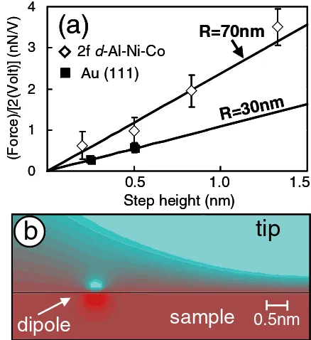
Results from measurements using the polarity-dependent component of the force (i.e., the difference between forces at V and V bias, divided by 2jVj) at steps of various heights are shown in Fig. 4(a). As can be seen, the experimental points follow a straight line. To determine the magnitude of the step dipole moment we compute the electrostatic force using the Generalized Image Charge Method(GICM) program [20,21], a varia-tional method for solving electrostatic problems that is particularly efficient for problems with high symmetry. The tip is modeled by a sphere of radiusR, which is an equipotential surface produced by a series of point charges qi and dipolespi at fixed positionsrj within the sphere. The magnitudes of the charges are adjusted to reproduce the boundary conditions of a constant potentialVat radius R, and the sample surface at ground. With a suitable choice of positions, a relatively small number of point charges (less than 10) can reproduce the potential over the surface
of the sphere within 1%. In this method the relative positions of the point charges and dipoles within the tip are fixed — only the magnitudes of the charges are changed as the tip-sample geometry is changed. For the present geometry, six point charges were distributed along the surface normal between the center and the sphere bound-ary, plus two symmetrical pairs of point dipoles located off axis in the plane defined by the surface normal and the line dipoleP. Once the effective charges were determined, the tip-sample forces were calculated as the sum of the forces between the point chargesqi,pi, their image chargesq0i,p0i
below the surface plane, and the fixed line dipole P. The field distribution calculated using these parameters is shown in Fig. 4(b).
The radii of the tips used for the Au and Al-Ni-Co samples derived from the force-distance curves was found to be3011 nmand7030 nm, respectively. Calcula-tions performed for several values of tip radius and for 0.5 nm for Dare shown in Fig. 4(a) as a function of step height and step dipole moment [22]. As we can see the data (difference in the force at and bias per unit applied volt) fit quite well the lines corresponding to step dipole values of 1:6 D=nm or 0:45 D=step atom for Au(111) monatomic steps [23] with the tip radius of 30 nm, and
-40 -30 -20 -10 0 10 20
-4 -2 0 2
Vertical displacement of piezo (nm)
n o rm a l fo rc e (n N ) -2 -1.5 -1 -0.5 0 0.5 1 cu rr e n t (n A ) 0 5 10 15 20 25
[image:5.612.326.545.357.596.2]0 1 2 3 1/D(1/nm) Fn(nN) D current force Electrostatic attraction
FIG. 3. Force and current-distance curves measured on Au(111) at a tip bias of3 V. Before contact the electrostatic force bends the tip towards the surface. This attraction is used to calculate the tip radius (inset), from the slope of F vs 1=D, yieldingR30 nm.
0 1 2 3 4 (F o rc e )/[2 (V o lt)] (n N /V )
R=70nm
R=30
nm
Step height (nm)
2f d-Al-Ni-Co
Au (111)
(a)
sample
tip
0.5nm
b
dipole
0.5 1.0 1.5
0 1 2 3 4 (F o rc e )/[2 (V o lt)] (n N /V )
R=70nm
R=30
nm
Step height (nm)
2f d-Al-Ni-Co
Au (111)
(a)
sample
tip
0.5nm
b
dipole
sample
tip
0.5nm
b
b
dipole
0.5 1.0 1.5
FIG. 4 (color online). (a) Difference in the force experienced by the tip at the steps for positive and negative bias, per unit applied volt nN=V. Open symbols correspond to steps on Al-Ni-Co quasicrystal surface. Filled symbols to steps on Au(111). The lines are calculations for 1 and 0.45 D per step atom, respectively; by definition they pass through the origin. The error bar is associated with the noise level of force measurement. (b) Electric field distribution calculated using the GICM in the tip-sample region with a permanent dipole close to the tip apex. (R30 nm,D0:5 nm.)
PRL95,136802 (2005) P H Y S I C A L R E V I E W L E T T E R S 23 SEPTEMBER 2005week ending
[image:5.612.54.296.472.650.2]2:5 D=nm or 1:0 D=step atom for the smallest (0.2 nm) quasicrystal steps with the tip radius of 70 nm. We can conclude that the dipole moment scales proportionally to step height, at least for steps up to 1.5 nm.
The dipole moment obtained for Au(111) is3times larger than the value of0:16 D=atom obtained by Jiaet al. [8] from STM barrier height measurements and2times larger than the 0.20 to0:27 D=atom obtained by Besocke et al. [2] from work-function measurements on stepped Au(111). Bartels et al. [24] obtained 0:33 D=atom for Cu(111) steps from STM spectroscopy of localized states at step edges. Apart from systematic and statistical errors in the measurements, the discrepancy could be related to the very different methods used, tunneling barrier in one case and average work function in another as compared to direct measurement of the dipole force field in the present work.
In conclusion, we have shown the existence of localized dipole fields in the vicinity of steps through direct mea-surements of the forces experienced by a biased STM tip. Together with measurements of the tip radius (from force-distance curves) and tip-sample force-distance (from current-distance approach curves) in the course of the same ex-periment, the method provides a direct way to map out and to measure local dipole moments on surfaces that should be of significance in studies of chemical and electronic prop-erties of surfaces.
This work was supported by the Director, Office of En-ergy Research, Office of Basic EnEn-ergy Sciences, Materials Sciences Division, of the U.S. Department of Energy through the Ames Laboratory, Contract No. W-405-Eng-82, and through Lawrence Berkeley National Laboratory, Contract No. DE-AC02-05CH11231. J. J. S. have been supported by the EU Integrated Project ‘‘Molecular Imaging’’ (Contract No. LSHG-CT-2003-503259). G. M. S. acknowledges support from the Spanish Ministerio de Educacio´n y Ciencia.
*Author to whom correspondence should be addressed. Electronic mail: mbsalmeron@lbl.gov
[1] R. Smoluchowski, Phys. Rev.60, 661 (1941).
[2] K. Besocke and H. Wagner, Phys. Rev. B8, 4597 (1973). [3] B. Kral-Urban, E. A Niekisch, and H. Wagner, Surf. Sci.
64, 52 (1977).
[4] K. Besocke, B. Krahl-Urban, and H. Wagner, Surf. Sci.68, 39 (1977).
[5] H. Ishida and A. Liebsch, Phys. Rev. B46, 7153 (1992). [6] R. Stumpf and M. Scheffler, Phys. Rev. B53, 4958 (1996). [7] B. Marchon, D. F. Ogletree, and M. Salmeron, J. Vac. Sci.
Technol. A6, 531 (1988).
[8] J. F. Jia, K. Inoue, Y. Hasegawa, W. S. Yang, and T. Sakurai, Phys. Rev. B58, 1193 (1998).
[9] T. Arai and M. Tomitori, Appl. Surf. Sci. 157, 207 (2000).
[10] M. Guggisberg, M. Bammerlin, A. Baratof, R. Lu¨thi, Ch. Lopacher, F. M. Battison, J. Lu¨, R. Bennewitz, E. Meyer, and H.-J. Gu¨ntherodt, Surf. Sci.461, 255 (2000). [11] J. Y. Park et al., Phys. Rev. B 71, 144203 (2005);
M. Enachescuet al., Phys. Rev. Lett.81, 1877 (1998). [12] NT-MDT Co., Zelenograd Research Institute of Physical
Problems, Moscow, Russia.
[13] J. Y. Parket al., Appl. Phys. Lett.86, 172105 (2005). [14] J. D. Jackson, Classical Electrodynamics (J. Wiley,
New York, 1975). The scaling relations are equivalent to the problem treated in Sect. 2.4 of a fixed charge and a biased conducting sphere.
[15] RHK Technology, Troy, MI USA, Model No. UHV-350. [16] I. R. Fisher, M. J. Kramer, Z. Islam, A. R. Ross,
A. Kracher, T. Wiener, M. J. Sailer, A. I. Goldman, and P. C. Canfield, Philos. Mag. B79, 425 (1999).
[17] J. Y. Park, D. F. Ogletree, M. Salmeron, C. J. Jenks, and P. A. Thiel, Tribol. Lett.17, 629 (2004).
[18] M. Kishida, Y. Kamimura, R. Tamura, K. Edagawa, S. Takeuchi, T. Sato, Y. Yokoyama, J. Q. Guo, and A. P. Tsai, Phys. Rev. B65, 094208 (2002).
[19] G. M. Sachaet al., Appl. Phys. Lett.86, 123101 (2005). [20] G. Mesa, E. Dobado-Fuentes, and J. J. Sa´enz, J. Appl.
Phys.79, 39 (1996).
[21] S. Go´mez-Mon˜ivas, L. S. Froufe-Pe´rez, A. J. Caaman˜o, and J. J. Sa´enz, Appl. Phys. Lett.79, 4048 (2001). [22] The origin0;0is a valid point because the force through
a zero height step is obviously zero.
[23] One debye1018 esucm 3:361030 Cm
0:39 eawhereais the Bohr radius andethe electron
charge.
[24] L. Bartels, S. W. Hla, A. Ku¨hnle, G. Meyer, K.-H. Rieder, and J. R. Manson, Phys. Rev. B67, 205416 (2003).