Electrical and Computer Engineering Publications
Electrical and Computer Engineering
2013
Growth and characterisation of Gd5(SixGe1−x)4
thin film
Ravi L. Hadimani
Iowa State University, [email protected]
Cajetan Ikenna Nlebedim
Iowa State University, [email protected]
Y. Melikhov
Cardiff University
David C. Jiles
Iowa State University, [email protected]
Follow this and additional works at:
http://lib.dr.iastate.edu/ece_pubs
Part of the
Electromagnetics and Photonics Commons
The complete bibliographic information for this item can be found at
http://lib.dr.iastate.edu/
ece_pubs/29
. For information on how to cite this item, please visit
http://lib.dr.iastate.edu/
howtocite.html
.
Growth and characterisation of Gd5(SixGe1−x)4 thin film
Abstract
We report for the first time successful growth of magnetic thin films containing the Gd5(Six Ge1−x)4 phase, which is expected to show giant magnetocaloric properties. The film wasdeposited by Pulsed Laser
Deposition (PLD) on a (001) silicon wafer at 200 °C from a polycrystalline Gd5Si2.09 Ge 1.91 target prepared by arc melting. PLD was achieved using a femto second laser with a repetition rate of 1 kHz, and a pulse energy of up to 3.5 mJ. The average film thickness was measured to be 400 nm using a Scanning Electron Microscopy and the composition of the film was analyzed using Energy Dispersive Spectroscopy and found to be close to the target composition. X-Ray Diffraction analysis confirmed the presence of Gd5Si2Ge 2
monoclinic structure. Magnetic moment vs. magnetic field measurement confirmed that the film was
ferromagnetic at a temperature of 200 K. The transition temperature of the film was determined from a plot of magnetic moment vs. temperature. The transition temperature was between 280 and 300 K which is close to the transition temperature of the bulk material.
Keywords
Ames Laboratory, Germanium, Pulsed laser deposition, Thin films, Magnetic films, Magnetic moments
Disciplines
Electromagnetics and Photonics
Comments
The following article appeared inJournal of Applied Physics113 (2013): 17A935 and may be found at
http://dx.doi.org/10.1063/1.4799975.
Rights
Copyright 2013 American Institute of Physics. This article may be downloaded for personal use only. Any other use requires prior permission of the author and the American Institute of Physics.
Growth and characterisation of Gd5(SixGe1x)4 thin film
R. L. Hadimani, I. C. Nlebedim, Y. Melikhov, and D. C. JilesCitation: Journal of Applied Physics 113, 17A935 (2013); doi: 10.1063/1.4799975
View online: http://dx.doi.org/10.1063/1.4799975
View Table of Contents: http://scitation.aip.org/content/aip/journal/jap/113/17?ver=pdfcov
Published by the AIP Publishing
Articles you may be interested in
Growth and characterization of Pt-protected Gd5Si4 thin films J. Appl. Phys. 115, 17C113 (2014); 10.1063/1.4865322
Large magnetocaloric effect and refrigerant capacity near room temperature in as-cast Gd5Ge2Si2xSnx compounds
Appl. Phys. Lett. 102, 192410 (2013); 10.1063/1.4806971
Magnetocaloric effect in layer structural Gd 5 ( Si x Ge 1 x ) 4 Gd composite material J. Appl. Phys. 101, 09C520 (2007); 10.1063/1.2712298
The effects of small metal additions ( Co , Cu , Ga , Mn , Al , Bi , Sn ) on the magnetocaloric properties of the Gd 5 Ge 2 Si 2 alloy
J. Appl. Phys. 99, 08K908 (2006); 10.1063/1.2173632
Thermal Property of DyxEr1xAl2 and Gd5(SixGe1x)4 for Hydrogen Magnetic Refrigeration AIP Conf. Proc. 711, 11 (2004); 10.1063/1.1774546
Growth and characterisation of Gd
5(Si
xGe
12x)
4thin film
R. L. Hadimani,1,2,a)I. C. Nlebedim,2,1Y. Melikhov,3and D. C. Jiles1,2 1
Department of Electrical and Computer Engineering, Iowa State University, Ames, Iowa 50011, USA
2
Ames Laboratory, US Department of Energy, Iowa State University, Ames, Iowa 50011, USA
3
Wolfson Centre for Magnetics, Cardiff University, Cardiff CF24 3AA, United Kingdom
(Presented 16 January 2013; received 1 November 2012; accepted 24 January 2013; published online 9 April 2013)
We report for the first time successful growth of magnetic thin films containing the Gd5(SixGe1 x)4 phase, which is expected to show giant magnetocaloric properties. The film was deposited by Pulsed Laser Deposition (PLD) on a (001) silicon wafer at 200 C from a polycrystalline Gd5Si2.09Ge1.91 target prepared by arc melting. PLD was achieved using a femto second laser with a repetition rate of 1 kHz, and a pulse energy of up to 3.5 mJ. The average film thickness was measured to be 400 nm using a Scanning Electron Microscopy and the composition of the film was analyzed using Energy Dispersive Spectroscopy and found to be close to the target composition. X-Ray Diffraction analysis confirmed the presence of Gd5Si2Ge2 monoclinic structure. Magnetic moment vs. magnetic field measurement confirmed that the film was ferromagnetic at a temperature of 200 K. The transition temperature of the film was determined from a plot of magnetic moment vs. temperature. The transition temperature was between 280 and 300 K which is close to the transition temperature of the bulk material.VC 2013 American Institute of Physics. [http://dx.doi.org/10.1063/1.4799975]
I. INTRODUCTION
Magnetocaloric Gd5(SixGe1 x)4has been studied exten-sively, since the giant magnetocaloric effect was discovered by Pecharskyet al.1Various other rare earth materials were also studied by the same group in search of even higher giant magnetocaloric effect.2Bruck et al.reported giant magneto-caloric effect in non-rare earth materials (MnFeP0.45As0.55) at room temperature.3 There has been extensive work on bulk magnetocaloric materials1–7 but there are fewer reports on thin films or other nanostructured magnetocaloric materials, although thin films of magnetocaloric materials have potential applications in micro-cooling in ICs and MEMS. Sambandam
et al.8reported unsuccessful growth of Gd5Si2Ge2thin film at a higher temperature of 750–1150 C using sputtering tech-nique on a silicon nitride wafer.
In this paper we report successful growth of magnetic thin film of Gd5Si2.09Ge1.91 using Pulsed Laser Deposition (PLD) technique and its structural and magnetic characteri-zation. The film’s microstructure including the thickness was analyzed using Scanning Electron Microscopy (SEM) and the composition was determined by Energy Dispersive Spectroscopy (EDS). Magnetic measurements and X-ray dif-fraction (XRD) of the film were also analyzed.
II. SAMPLE PREPARATION AND EXPERIMENTAL DETAILS
A polycrystalline Gd5Si2.09Ge1.91 sample prepared by arc melting using commercial grade gadolinium was used as a target in the pulsed laser deposition. Spectra Physics’ Solstice femtosecond laser with a repetition rate of 1000 Hz, pulse energy of up to 3.5 mJ, and a nominal beam diameter
of 7 mm before being focused was used for the deposition. The film was deposited on a (001) silicon wafer at 200 C at a pressure of 1.210 6Torr. The deposition was carried out for 20 min. The rate of deposition was estimated from the thick-ness measurement and found to be 20 nm/s. Microstructure and composition analyses were carried out using SEM and EDS, respectively. Secondary Electron (SE) detector and Back Scattered Electron (BSE) detectors were used during SEM imaging. XRD was carried out in the PANanalytical equip-ment with a Cu X-ray tube. The XRD data were analyzed in
X’PERT HIGHSCOREsoftware. Magnetization measurements were
carried out on a SQUID magnetometer.
III. RESULTS AND DISCUSSIONS
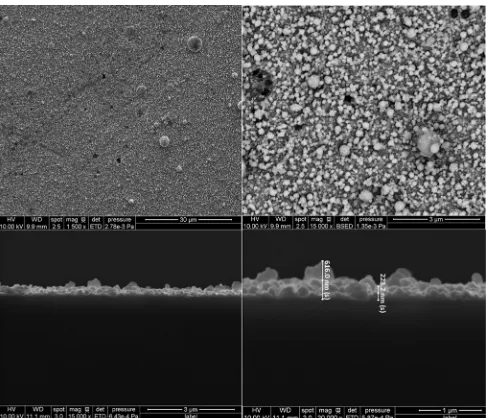
Figs.1(a)and1(b)show SE and BSE images of the film at magnifications at 1500and 15000, respectively. The deposition shows a continuous film with varying sizes of spherical droplets which is the characteristic of PLD deposi-tion of metallic thin films. Femtosecond laser was chosen for this deposition as the shorter pulse width produce smaller droplets and smoother films.9With a repetition rate of 1000, higher deposition rate is achieved at lesser time which helps to obtain similar phase material to the target material. BSE image shows most of the top grains in one gray level and the grains in the bottom layer with a different grey level. This variation in the contrast between the grains at different thick-ness of the film may be due to different phases of the mate-rial. However, another reason could be that variation in the distance between grains and the detector also results in dif-ferent contrast in the BSE image. Fig.1(c)shows the cross-section of the film that is continuous at 15000 magnifica-tion. Thickness of the film was measured at 30000
magnification as shown in Fig.1(d). Minimum thickness was measured to be 232 nm and maximum was 616 nm. Using the
a)Author to whom correspondence should be addressed. Electronic mail: [email protected]
0021-8979/2013/113(17)/17A935/3/$30.00 113, 17A935-1 VC2013 American Institute of Physics
thickness measured from Fig.1(d)the deposition rate was esti-mated to be 20 nm/s. EDS was carried out at three different locations on the film. The locations were chosen on three spherical particles of different sizes. Peaks of Gd, Si, and Ge from all the three spherical particles match closely with respect to the intensity suggesting similar composition. TableIshows quantitative analysis of composition, where the K(1.74 keV), K(9.8 keV), and L(6.05 keV) lines of silicon, germanium, and gadolinium were used for quantification. The composition of the film was similar to the composition of the target. The L line of germanium and the M line of gadolinium overlap at 1.2 keV, which cannot be used for quantification of composi-tion, hence the K line of germanium and the L line of gadolinium were used. In order to get the K line (9.8 keV) of germanium the accelerating voltage of the electron should be about 15 kV. Electrons penetrate into the wafer when the accelerating voltage of the electron is high and EDS detector detects x-rays that are emitted by the wafer.CASINOsimulation
software was used to determine the thickness of the film such that minimum number of electrons penetrates into the substrate which was determined to be about 150 nm for our parameters.
XRD analysis of thin film of Gd5Si2.09Ge1.91was carried out at room temperature.X’PERT HIGHSCORE PLUSsoftware was
used to identify and match the peaks. This search and match function indicated the presence of other phases such as Gd5Si4and Gd5Ge3as shown in TableII.
Magnetic moment vs. temperature was measured at an applied field of 100 Oe (7.9 kA/m) as shown in Fig. 2(a),
with its derivative shown in Fig.2(b). It can be seen that there is a constant slope below 280 K and then its value increases from 280 K to 300 K indicating that there is a phase transition occurring between these temperatures.10,11 The volume frac-tion of the monoclinic phase was estimated from the magnetic moment variation at the transition temperature and found to be 11% of the original material considering that other phases do not have a transition temperature below 200 K.
[image:5.612.53.296.61.270.2]FIG. 1. (a) Secondary electron image at 1500, (b) BSE image at 15000, (c) cross section of thin film at 15000, and (d) thickness measurement on cross section at 30000.
TABLE I. Composition of the film averaged from 3 locations.
Element Line type Wt. % Wt. % sigma At. %
Si K 6 0.12 23
Ge K 14 0.75 22
Gd L 80 0.71 55
[image:5.612.315.561.86.156.2]Total: 100.0 100.0
TABLE II.X’PERT HIGHSCORE PLUSmatched structures of Gd5Si2Ge2Gd5Ge3 and Gd5Si4.
Ref. code Score Compound name Scale factor Chem formula
01-087-2320 24 Gadolinium silicide germanide
0.317 Gd5(Si2Ge2)
00-026-1421 14 Gadolinium germanium 0.283 Gd5Ge3 01-087-2319 21 Gadolinium silicide 0.512 Gd5Ge4
FIG. 2. (a) m vs. T at an applied field of at 100 Oe (7.9 kA/m). (b) Derivative of Fig.2(a)showing the start and end of the phase transition. Inset figure shows the transition temperature of bulk sample of Gd5Si2.09Ge1.91.
FIG. 3. m vs.l0H at 200 K showing the ferromagnetic nature of the material inset figure shows m vs. H measurement at 270 K on bulk sample of Gd5Si2.09Ge1.91.
17A935-2 Hadimaniet al. J. Appl. Phys.113, 17A935 (2013)
[image:5.612.314.561.183.389.2] [image:5.612.325.548.555.731.2] [image:5.612.50.299.692.765.2]The transition temperature of the same composition measured on the bulk material at the same 100 Oe (7.9 kA/m) is between 270 K and 300 K as shown in the inset. Fig. 3
shows magnetic moment vs. magnetic field at 200 K. It can be seen that the sample is ferromagnetic and saturates below 0.5 T (0.39 MA/m). The inset shows the magnetization of the bulk sample with composition Gd5Si2.09Ge1.91at 270 K which also saturates at a similar magnetic field.
IV. CONCLUSION
A magnetic thin film of Gd5(SixGe1 x)4phase was suc-cessfully grown for the first time that is expected to show giant magnetocaloric properties. Its microstructure was ana-lyzed using SEM. The composition of the film was deter-mined by EDS using non-overlapping principal lines. XRD analysis confirmed the presence of monoclinic Gd5Si2Ge2 structure. The magnetic moment vs. temperature measure-ments on a thin film and a bulk sample showed similar phase transition temperatures. Magnetic moment vs. magnetic field measurements on thin film and bulk samples also showed that saturation is reached at similar values of magnetic field.
ACKNOWLEDGMENTS
This work at the Ames Laboratory was supported by the DOE-Basic Energy Sciences under Contract No.
DE-AC02-07CH11358 and Barbara and James Palmer Endowment at the Department of Electrical and Computer Engineering of Iowa State University. The authors acknowl-edge the contributions of A. H. Shaw and K. W. Dennis Ames Laboratory, US DOE for helping with the PLD and SQUID measurements, respectively.
1
V. K. Pecharsky and K. A. Gschneidner, Jr., Appl. Phys. Lett. 70, 3299–3301 (1997).
2
V. K. Pecharsky and K. A. Gschneidner, Jr.,J. Magn. Magn. Mater.200, 44–56 (1999).
3
O. Tegus, E. Bruck, K. H. J. Buschow, and F. R. de Boer,Nature415, 150–152 (2002).
4L. Morellon, P. A. Algarabel, M. R. Ibarra, J. Blasco, B. Garcıa-Landa, Z. Arnold, and F. Albertini,Phys. Rev. B58, R14721 (1998).
5
R. L. Hadimani and D. C. Jiles,IEEE Magn. Lett.1, 6000104 (2010). 6
R. L. Hadimani, Y. Melikhov, J. E. Snyder, and D. C. Jiles,J. Appl. Phys.
103, 033906 (2008).
7A. M. Pereira, E. Kampert, J. M. Moreira, U. Zeitler, J. H. Belo,
C. Magen, P. A. Algarabel, L. Morellon, M. R. Ibarra, J. N. Gonc¸alves, J. S. Amaral, V. S. Amaral, J. B. Sousa, and J. P. Araujo,Appl. Phys. Lett.
99, 132510 (2011).
8S. N. Sambandam, B. Bethala, D. K. Sood, and S. Bhansali,Surf. Coat.
Technol.200, 1335–1340 (2005). 9
P. Lu, Y. Zhou, Q. Zheng, and G. Yang, Phys. Lett. A350, 293–296 (2006).
10R. L. Hadimani, P. A. Bartlett, Y. Melikhov, J. E. Snyder, and D. C. Jiles,
J. Magn. Magn. Mater.323, 532–534 (2011). 11
R. L. Hadimani, Y. Melikhov, J. E. Snyder, and D. C. Jiles,IEEE Trans. Magn.45, 4368–4371 (2009).