n
‑
Type Doping of Organic Semiconductors: Immobilization via
Covalent Anchoring
Patrick Reiser,
§,∥,‡Frank S. Benneckendorf,
∥,⊥,‡Marc-Michael Barf,
∥,#Lars Mu
̈
ller,
∥,#Rainer Ba
̈
uerle,
∥,∇Sabina Hillebrandt,
∥,∇,†Sebastian Beck,
∥,∇Robert Lovrincic,
∥,#Eric Mankel,
§,∥Jan Freudenberg,
∥,⊥Daniel Ja
̈
nsch,
∥,⊥Wolfgang Kowalsky,
∥,#,∇Annemarie Pucci,
∥,∇Wolfram Jaegermann,
§,∥Uwe H. F. Bunz,
∥,⊥and Klaus Mu
̈
llen
*
,∥,○§Materials Science Department, Surface Science Division, TU Darmstadt, Otto-Berndt-Straße 3, 64287 Darmstadt, Germany
∥InnovationLab, Speyerer Straße 4, 69115 Heidelberg, Germany
⊥Organisch-Chemisches Institut, Ruprecht-Karls-Universität Heidelberg, Im Neuenheimer Feld 270, 69120 Heidelberg, Germany
#Institute for High-Frequency Technology, TU Braunschweig, Schleinitzstraße 22, 38106 Braunschweig, Germany
∇KirchhoffInstitute for Physics, Heidelberg University, Im Neuenheimer Feld 227, 69120 Heidelberg, Germany
○Max Planck Institute for Polymer Research, Ackermannweg 10, 55128 Mainz, Germany
*
S Supporting InformationABSTRACT: Electrical doping is an important tool in the design of organic devices to modify charge carrier concentration in and Fermi level position of organic layers. The undesired diffusion of dopant molecules within common transport materials adversely affects both lifetime and device performance. To overcome this drawback, we developed a strategy to achieve immobilization of dopants through their covalent attachment to the semiconductor host molecules. Derivatization of the commonly employed n-type dopant 2-(2-methoxyphenyl)-1,3-dimethyl-2,3-dihydro-1H -ben-zoimidazole (o-MeO-DMBI) with a phenylazide enables the resultingo-AzBnO-DMBIto photochemically generate a reactive nitrene, which subsequently binds covalently to the host material,
6,6-phenyl-C61-butyric acid methyl ester (PCBM). Both the activation and addition reactions are monitored by mass spectrometry as well as optical and photoelectron spectroscopy. A suppression of desorption and a decrease in volatility of the DMBI derivative in ultrahigh vacuum were observed after activation of a bilayer structure of PCBM and o-AzBnO-DMBI. Electrical measurements demonstrate that the immobilized o-AzBnO-DMBI can (i) dope the PCBM at conductivities comparable to values reported for o-MeO-DMBI in the literature and (ii) yield improved electrical stability measured in a lateral two terminal device geometry. Our immobilization strategy is not limited to the specific system presented herein but should also be applicable to other organic semiconductor−dopant combinations.
■
INTRODUCTIONThe applications and benefits of electrical or electrochemical doping in organic semiconductors are manifold.1,2 Suitable dopants increase the conductivity of organic layers by several orders of magnitude, for example, in charge transport layers of organic light-emitting diodes (OLEDs).3 Promising thermo-electric devices can be realized with doped conjugated polymers due to their low thermal conductivity.4−6 Most importantly, doped layers enable quasi-ohmic contacts to metal electrodes, which greatly improves charge carrier injection and mitigates contact resistances due to offsets in energy level alignment.7−9 A prerequisite for applying doped layers in dedicated device stacks is stability since diffusion of dopants into adjacent active layers has been identified as a degradation mechanism (e.g., exciton quenching), detrimental to photo-active devices.10−14 Moreover, diffusion of dopants can be
problematic in organic hole transport layers for planar perovskite solar cells.15 Consequently, stable and efficient doping of organic materials is of high interest in present-day device fabrication. Replacing atomic dopants such as halides or alkali metals by small molecular p- and n-type dopants reduces volatility significantly.16However, some host−dopant systems still exhibit diffusivity of organic electron donors/accept-ors.17,18 This effect is more pronounced within conjugated polymers compared to molecular host materials.19−21 Even though the dopant lacks diffusion in the host matrix, this might change when an electric field is applied. Recently, the migration of molecular dopants in an electric field has been
Received: March 22, 2019
Revised: May 14, 2019
Published: May 15, 2019
Article
pubs.acs.org/cm Cite This:Chem. Mater.2019, 31, 4213−4221
License, which permits unrestricted use, distribution and reproduction in any medium, provided the author and source are cited.
Downloaded by UNIV OF ST ANDREWS at 06:42:32:358 on June 28, 2019
Besides physical modifications such as size or morphology, increased intermolecular interaction also reduces the mobility of dopants. These include dispersion force, dipole−dipole interactions, π−π interactions, or even hybridization.28 Charged dopants are much less diffusive than neutral dopants due to electrostatic interactions.21,29A covalent bond between the dopant and the host molecule would allow much stronger “fixation” ideally for the immobilization of both neutral and charged dopants. A premodification of the host with a functional group that introduces self-doping was already used to localize dopants in assembled thin films.30,31 For the covalent bond formation after blending, the host and dopant have to have complementary functional groups.32−34 This concept requires modification of each transport material tofit the corresponding dopant, which is not practical given the plethora of materials in use. In order to be generally compatible with a wide scope of host materials, an anchor group for dopants needs an unspecific binding method, for example, by attachment to aliphatic C−H or olefinic CC bonds present in almost any organic semiconductor without introduction of severe degradation or traps. A practical solution for this issue can be derived from photochemical cross-linking as the desolubilization protocol:35The utilization of various bis-azides for cross-linking, thus preventing polymer strands from redissolution in solution-processed heterostruc-tures, is not limited to one specific polymer.36,37The azide is activated by deep-ultraviolet light (UV, 254 nm), inducing photolysis and generating reactive singlet nitrenes. When properly substituted, these predominantly insert into aliphatic CH bonds, and side reactions38 involving triplet pathways, aromatic insertion, attack upon other functional groups, or ketenimine ring expansion are suppressed.36,39,40The latter is found to be dominating only in solution for non-fluorinated aryl azides,39,41whereas in thinfilms or matrices, CH insertion prevails.42−45
1,3-Dimethyl-2-phenyl-2,3-dihydro-1H-benzoimidazole (DMBI) derivatives are effective, air-stable, and thus easy-to-handle, solution-processable n-type dopants. DMBIs are often used to dope n-channel semiconductors, preferably PCBM46−51 or n-type polymers.47,52 However, they seem to be more effective, in terms of achieved maximum conductivity, in combination with PCBM than with polymers like P(NDI2OD-T2) due to the poor miscibility of the dopant and polymer.6,47,53Although the doping mechanism of DMBI derivatives in, for example, PCBM has been investigated, it is still under debate.48,51,54 The initial step either involves a hydride transfer to the host or a hydrogen radical transfer with a subsequent electron transferboth mechanisms lead to the
mass spectrometry verifies a covalent linkage of the dopant to PCBM. Our immobilization strategy via nitrene generation is generally applicable and not limited to a specific host−dopant system. Furthermore, it is destined to improve the stability, lifetime, and performance of doped organic devices by ideally suppressing both detrimental diffusion and drift effects.
■
RESULTS AND DISCUSSIONSynthesis and Immobilization Reactions. DMBI dopants are easily accessible via simple condensation reactions according to Scheme 1. Introduction of a phenylazide is
achieved after etherification of salicylaldehyde employing 1-azido-4-(bromomethyl)benzene (1) in DMF at room temper-ature furnishing compound 2 in 85% yield, followed by condensation with N1,N2-dimethylbenzene-1,2-diamine to
afford o-AzBnO-DMBI in 40% yield. The characteristic IR absorption band of the azide stretching vibration at 2109 cm−1
(see Figure 4b and Figure S11) confirms the azide
functionalization.57
To elucidate the influence of the azide group on immobilization, we synthesized the non-azido-functionalized analogue and thus nonimmobilizableo-BnO-DMBIemploying benzyl bromide (3) for the Williamson ether synthesis. Both new dopants were isolated after crystallization from petroleum ether/methanol or DCM/hexane, respectively. The obtained colorless single crystals were suitable for X-ray crystal analyses, unambiguously proving their structure (see the Supporting
Information). In order to optimize the processing parameters,
we studied the stability of the newly synthesized dopants and the literature known o-MeO-DMBI in solution (see the Supporting Information, Figure S13). NMR spectroscopy revealed that the dopants are only fairly stable in solution: after 1 day at ambient conditions (sunlight and air) in chloroform, oxidized species can be seen. However, the dopant appears to be stable for processing within several hours. In the solid state at−10 °C, however, no degradation was observed over months.
In acetonitrile, the UV−vis spectrum of o-BnO-DMBI exhibits absorption features at λ = 221, 274, and 313 nm, whereas foro-AzBnO-DMBI, an additional absorption band at 253 nm is detected and attributed to the azide functional group
(Figure S14).42,58Irradiation at 254 nm excites the azide and
induces nitrene generation.42,45 Throughout this work, this wavelength is used to initiate the immobilization process. Thermogravimetric analysis (see Figure S15) of o -AzBnO-DMBIshows irreversible mass loss at 117°C corresponding to the extrusion of nitrogen. During additional heating/cooling cycles below the decomposition temperature of 240 °C, no further mass loss is observed. Similar to the azide-function-alized dopant, o-BnO-DMBI exhibits a rather low melting point at 108°C (86°C foro-AzBnO-DMBI) and decomposes at 200°C. To achieve maximum doping effects for the host/ DMBI blend, annealing at 75 °C is required.48 Thus, o -AzBnO-DMBI is stable enough to test the doping of the PCBM host upon thermal treatment.
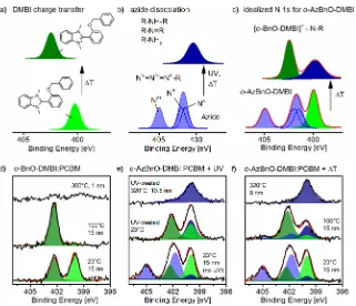
In the following, we provide spectroscopic data to corroborate successful anchoring of the o-AzBnO-DMBI dopant. From X-ray photoelectron spectroscopy (XPS) core-level spectra, we gain insight into the activation mechanism of both the dopant and the anchor group as well as possible decomposition reactions. In order to additionally test the thermal stability of the DMBI derivative in the blend, we annealed thinfilms of high doping concentration (50 mol %) in ultrahigh vacuum (UHV, 10−9mbar) and measured XPS at each temperature step (for details, seeFigure S20). The N 1s emission of o-AzBnO-DMBI contains a contribution of the functional azide group and the DMBI core, illustrated inFigure 1c in blue (azide) and in green (DMBI).
To assign the N 1s peak components of o-AzBnO-DMBI correctly, it is instructive to analyze spectral changes expected from DMBI and the azide group, sketched inFigures 1a and
[image:3.625.153.474.63.339.2]1b, respectively. The spectra of o-BnO-DMBI in Figure 1d only exhibit peak components of the DMBI core located at 402.5 and 400 eV. We identify the nitrogen emission at 402.5 eV as charged dopants having formed a radical and transferred an electron to PCBM. This assignment agrees with the N 1s emission of the ionic DMBI salt at about 402.5 eV reported in the literature.59With rising temperature, the peak component at 400 eV transforms into charged DMBI species at 402.5 eV, which correlates with an increase in conductivity observed for annealed PCBM films doped with DMBI. The N 1s signal reported for pure azides sketched in Figure 1b has three
Figure 1.XPS measurements of the N 1s core-level spectra of thermally annealed PCBMfilms doped witho-BnO-DMBIando-AzBnO-DMBIin panels (d−f). (a−c) Schematic cartoon of N 1s peak components and their transformation. (d) Recorded spectra of PCBM doped witho -BnO-DMBIfor different annealing temperatures. (e) N 1s signal of PCBM doped witho-AzBnO-DMBItogether with the spectrum measured after UV activation and after annealing of the UV-activatedfilm to 320°C. (f) Direct annealing of theo-AzBnO-DMBI/PCBMfilm without UV treatment.
The assignment of peak composition in panels (d−f) is inferred from contributions of DMBI in green and from the azide in blue. The expected peak components of DMBI upon charge transfer and decomposition of pure azide are sketched in panels (a) and (b), respectively. Foro -AzBnO-DMBI, both reactions of panels (a) and (b) can occur as illustrated in panel (c). The peak shapes of panels (a) and (b) arefitted to the data in panels (e−f) using a constrained model (see theSupporting Informationfor details). In the componentfit, there is already a considerable fraction of charged dopants in panels (d−f) and possibly dissociated azide in panels (e) and (f) at room temperature. The initialfilm thickness at room temperature is 15 nm and changes in panels (d−f) for higher temperatures.
of the doped PCBMfilm inFigure 1f, the N 1s emission at 405 eV disappears above 100 °C suggesting that the azide group becomes thermally activated and produces a nitrene. As a result, carbon−nitrogen bonds are formed causing an addi-tional N 1s emission at 400 eV, which persists at temperatures higher than 300 °C. At the same time, the DMBI part ofo -AzBnO-DMBIdonates an electron, similar to o-BnO-DMBI, thus transferring the peak component at 400 eV into the charged DMBI species at 402.5 eV. When reaching higher temperature in UHV, pure and o-BnO-DMBI-doped PCBM completely evaporate from the substrate at 300 and 200 °C, respectively. Interestingly, the film doped with o -AzBnO-DMBI is stable even beyond 300 °C, and only a partial decrease in coverage is observed. However, from the N 1s emission, we infer that the N 1s peak component at 402.5 eV, attributed to charged dopants, disappears almost completely above 210°C leaving only carbon−nitrogen bonds at 400 eV when approaching 320°C in Figure 1(for details, seeFigure
S20).
At room temperature, pure and untreatedo-AzBnO-DMBI is volatile under UHV conditions as observed by XPS. However, when o-AzBnO-DMBI is sequentially processed on top of PCBM in monolayer-range thickness, a desorption experiment in UVH at room temperature reveals that the anchoring ofo-AzBnO-DMBIalso appears to be quantitative, renderingo-AzBnO-DMBIcompletely resistant to desorption after UV activation (see the Supporting Information for details). A similar trend is observed for thicker bilayer structures, which means that in pure dopantfilmso -AzBnO-DMBI may also react with neighboring dopants (see Figure
S19).
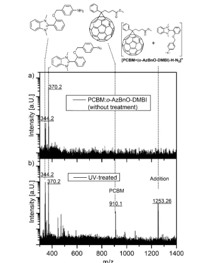
Concerning the anchoring mechanism, it is known that azides react with fullerenes in a 1,3-dipolar [3 + 2] cycloadditions affording triazolines,63,64 which, upon thermal treatment, undergo loss of nitrogen,65,66 or [2 + 1] cycloaddition with nitrenes yielding aziridinofullerenes or azafulleroids.67,68 Additionally, CH insertion into the alkyl chains of PCBM, though much less probable, may occur. To demonstrate covalent attachment of the dopant to the host, blends of o-AzBnO-DMBI and PCBM were analyzed by electrospray ionization (ESI) and matrix-assisted laser desorption ionization (MALDI) high-resolution mass spec-trometry. We prepared blends of PCBM ando-AzBnO-DMBI at 25 mol % in a solution of chlorobenzene, which were subsequently dried in vacuo. Azide activation was achieved by either annealing at 135°C or UV activation of spin-cast thin
films, which were redissolved, and the material was dried afterward. Whereas no [3 + 2] cycloaddition products are
is the more benign method as shown in the ESI spectra (Figure S25); fragmentation of the ether bond within the thermal activated blends is detected. We find comparably small mass peaks for amines (these may also be a fragment of mass spectroscopy created during ionization)69,70 and unreacted azide from the UV-activated blends (Figure 2). We attribute the latter to the slightly modified sample preparation for mass spectroscopy because XPS and IR experiments (Figures 3and
4, respectively) demonstrate quantitative azide photolysis.
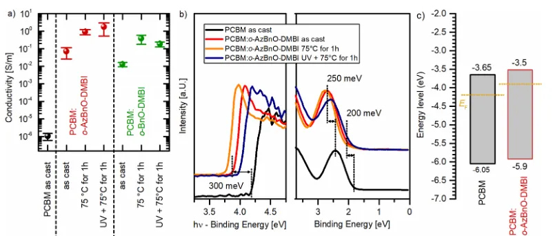
Doping and Functional Characterization. The con-ductivity measurements were performed under nitrogen on pure and doped PCBM layers (host-to-dopant ratio, 10:1), spin-cast from chlorobenzene onto prestructured silver contacts on glass substrates (Figure 3a and Figure S17). Whereas neat PCBM thin films exhibit conductivities in the range of 10−6S/m, this characteristic value rises up to 0.1 and
0.01 S/m for as-castfilms doped witho-AzBnO-DMBIando -BnO-DMBI, respectively. The final annealing step for doped
[image:4.625.335.541.132.402.2]films at 75 °C increases the conductivity further to 1 S/m. After UV treatment (254 nm) of as-cast films, the conductivities of the doped PCBM layers decrease by roughly half an order of magnitude in comparison to as-cast blends. The subsequent thermal treatment (1 h at 75°C) increases the
conductivities for both dopants by more than 2 orders of magnitude to 1 S/m. In total, this is a gain of 6 orders of magnitude compared to neat PCBM layers (seeFigure 3a).
UV photoelectron spectroscopic (UPS) measurements of corresponding PCBM layers on silicon are presented inFigure 3b. The secondary electron cutoffs ofo-AzBnO-DMBI-doped PCBM reveal strong shifts, which translate to a reduction of the work function of about 300 meV compared to the neat PCBM layer. Additionally, in doped layers, the highest occupied molecular orbital (HOMO) broadens, and the HOMO maximum shifts by 250 meV to higher binding energies compared to undoped PCBM and is accompanied by a shift of the core-level emission lines (see Figure S19). For comparison, Naab et al. observed a Fermi level shift of 500 meV in a PCBM blend with 1 wt %o-MeO-DMBIon ITO.51 The Fermi level shift goes along with an increase of free charge carrier concentration and thus leads to an increased conductivity revealing a strong n-type doping effect of both DMBI derivatives in PCBM. Annealing of the thinfilm results in an additional shift of the Fermi level toward the LUMO of about 50−100 meV for o-AzBnO-DMBI arriving at a total 350−400 meV shift. Furthermore, wefind a broadening of the emission of the HOMO level, yielding an increase of tail states
[image:5.625.114.515.63.234.2]for doped PCBMfilms. The results of the UPS measurements were used to calculate the energy level diagrams of pure and doped PCBM layers that are depicted inFigure 3c, assuming a constant band gap of about 2−2.5 eV.71−73
Figure 4a showsI−Vcurves of dopedo-AzBnO-DMBIand
o-BnO-DMBIPCBM layers as-cast and after UV treatment. At high electric field strength, the untreated films including o -AzBnO-DMBI feature a pronounced rise and subsequent falloffin current. As a result, theI−Vcurve displays a distinct hysteresis, which can be also observed when repeating the cycle (slightly shifted to higher voltages). This can be explained either by contact modification and/or by ionic migration. A drift of charged dopant molecules away from a contact causes a similar hysteresis in I−V curves, which was found for films of poly(3-hexylthiophen-2,5-diyl) (P3HT) doped with the p-dopants 2,3,5,6-tetrafl uoro-7,7,8,8-tetracya-noquinodimethane (F4TCNQ) and molybdenum tris[1-(methoxycarbonyl)-2-(trifluoromethyl)-ethane-1,2-dithiolene] (Mo(tfd-CO2Me)3)).22On the other hand, the I−Vcurve of
an o-AzBnO-DMBI doped layer that was UV-treated
(followed by a final annealing step) displays no or reduced hysteresis on average. This observation is afirst indication for a successful dopant immobilization after nitrene generation.
[image:5.625.103.566.292.452.2]Figure 3.(a) Conductivities of pure and doped PCBM layers with a molar doping ratio of 10:1 as-cast, after UV treatment, and after subsequent annealing. (b) UPS spectra of pure and doped PCBM layers with a molar doping ratio of 10:1 as-cast, after UV treatment, and after subsequent annealing. The secondary electron cutoffwith respect to the vacuum level and the HOMO onset with respect to the Fermi level are given. (c) Calculated energy levels of pure and doped PCBM layers with a band gap of 2.4 eV.
Figure 4.(a)I−Vcurves of annealed layers as-cast and after UV treatment. (b) Relative IR transmission spectra of 30 nm thick pure and doped PCBM layers with a molar doping ratio of 10:1. The spectra were measured on as-cast layers and after UV treatment as given in the legend. Dividing the spectra after the UV treatment by the as-cast spectra reveal the relative spectral change caused by the UV treatment. The vibrational mode of the azide group at 2109 cm−1is marked in panel (b) and strongly reduced by the UV treatment.
of PCBM layers doped witho-AzBnO-DMBIbefore and after UV treatment are presented inFigure 4b (see theSupporting
Information for additional spectra). Due to the doping
concentration of 10 mol %, most of the observed vibrational modes stem from PCBM and fail to reveal a change caused by the UV treatment. Only the characteristic vibrational mode of the dopant’s azide group at 2109 cm−1 vanishes completely, revealing a quantitative activation and dissociation of the azide by UV light.
■
CONCLUSIONSIn this work, we detail the synthesis of o-AzBnO-DMBI, a derivative of the literature known o-MeO-DMBI. An azidophenyl group is introduced to DMBI by etherification of salicylaldehyde employing 1-azido-4-(bromomethyl)-benzene and a subsequent condensation with N1,N2 -dimethylbenzene-1,2-diamine. The modification of DMBI with a reactive azide aims at providing a universally applicable anchor-like functional group, which should be able to covalently bind to a wide scope of common organic semiconductors. By creating a covalent bond with the host material, the dopant is expected to be immobilized or at least rendered significantly less mobile, which ideally reduces problems in devices arising from diffusion or drift of dopants. In an exemplary study, o-AzBnO-DMBI was blended with PCBM and activated by UV light in order to generate highly reactive nitrenes to ultimately form covalent carbon−nitrogen bonds between PCBM and the dopant. The azide activation was monitored by infrared and photoelectron spectroscopy. High-resolution mass spectrometry reveals addition products,
firmly demonstrating the covalent attachment of the dopant to PCBM molecules. The thermal stability ofo-AzBnO-DMBIin the blend was tested by annealing thinfilms of high doping concentration in UHV and by measuring temperature-dependent XPS. We find that the activated dopant renders the dopedfilm more resistant to desorption when approaching the desorption temperature of PCBM in UHV. At room temperature, activation of o-AzBnO-DMBI in a bilayer structure was shown to prevent desorption from PCBM under UHV. I−V measurements further prove that UV-activated o-AzBnO-DMBI maintains its doping properties giving rise to conductivities typical for blends of DMBI and PCBM. At high electricfield strength, the UV-activated doped PCBM films show no or neglectable hysteresis, but a pronounced hysteresis is observed if o-AzBnO-DMBI is not exposed to UV light. The increased electrical stability can be explained by a suppression of dopant drift due to anchoring of the dopant to PCBM after activation.
■
Synthesis. All reactions requiring exclusion of oxygen and moisture were carried out in heat-gun-dried glassware under a dry and oxygen-free nitrogen or argon atmosphere using Schlenk and glovebox techniques. All reagents were obtained from commercial suppliers and were used without further purification if not otherwise stated. Deuterated solvents were purchased from Sigma-Aldrich Laborchemikalien GmbH (Seelze, Germany).Sample Preparation for Analysis.If not noted otherwise, the dopants and PCBM were dissolved separately in chlorobenzene at a concentration of 5 g L−1 for XPS and 10 g L−1 for IR/I−V
measurements and were mixed right before spin-coating. The dopants were kept in solution for 5−10 min, but the PCBM solution was stirred overnight at 50°C. Thefilms were spin-coated at 1000 rpm for 60 s in a nitrogen glovebox on a cut n-doped silicon wafer for XPS, intrinsic silicon for IR, and on glass forI−Vmeasurements. Activation by UV light was performed with a GPH135T5L/4 mercury-vapor lamp from Peschl Ultraviolet with a nominal UV-C power of 1.2 W at 254 nm in the glovebox. The penlight was mounted on a stand at a distance of 10 cm above the sample. We measured the UV intensity at the sample position using a Newport power meter 1936-C equipped with a 818-UV photodiode plus attenuator and obtain a power density of 0.8 mW cm−2for a 20 min exposure time.
IR Spectroscopy.For IR transmission measurements, a Fourier transform IR spectrometer (Vertex 80v, Bruker) was used. To prevent absorptions from ambient air (H2O and CO2), the spectrometer was
evacuated to 3 mbar. All samples were recorded near normal transmittance (7°) with an MCT detector and a resolution of 4 cm−1.
For each spectrum, 200 scans were averaged.
Electrical Measurements. I−V measurements were performed under a nitrogen atmosphere at room temperature. For this purpose, finger-like structured silver contacts with channel lengths between 25 and 30μm were used. Voltages were applied on these contacts using the 4155C semiconductor parameter analyzer by Agilent Technolo-gies, which reads out corresponding currents for conductivity determination. Conductivities were then calculated from a set of at least three different samples.
Photoelectron Spectroscopy. Photoelectron spectroscopy (PES) measurements were carried out using a PHI5000 VersaProbe scanning photoelectron spectrometer, which was equipped with a monochromated Al KαX-ray source at 1486.7 eV photon energy for X-ray photoelectron spectroscopy (XPS) and a differentially pumped helium discharge lamp operated to achieve He I emission at 21.2 eV photon energy for ultraviolet photoelectron spectroscopy (UPS). The focused X-ray spot was approximately 200μm in diameter and was moved to a different position on the sample for longer acquisition in order to avoid radiation damage.
■
ASSOCIATED CONTENT*
S Supporting InformationThe Supporting Information is available free of charge on the
ACS Publications website at DOI:
10.1021/acs.chemma-ter.9b01150.
Synthesis, NMR spectroscopy, crystal structure, IR spectroscopy, NMR stability test, UV−vis absorption, TGA/DSC, ESI mass spectra, and XPS analysis (PDF)
■
AUTHOR INFORMATIONCorresponding Author
*E-mail:muellen@mpip-mainz.mpg.de.
ORCID
Lars Müller:0000-0001-7321-4702 Sebastian Beck: 0000-0003-2194-6842 Robert Lovrincic:0000-0001-5429-5586 Eric Mankel:0000-0001-6566-157X Annemarie Pucci:0000-0002-9038-4110 Uwe H. F. Bunz: 0000-0002-9369-5387 Klaus Müllen: 0000-0001-6630-8786 Present Address
†University of St Andrews, North Haugh, St Andrews KY16
9SS, United Kingdom.
Author Contributions
‡P.R. and F.S.B. contributed equally.
Notes
The authors declare no competingfinancial interest.
■
ACKNOWLEDGMENTSWe gratefully acknowledge the German Federal Ministry of Education and Research (BMBF) forfinancial support within the InterPhase project (FKZ 13N13659, 13N13656, 13N13657, and 13N13658). We thankfully acknowledge the mass spectroscopy data acquired by the Mass Spectroscopy Facility at OCI Heidelberg under the supervision of Dr. J. Gross. We thank Dr. Frank Rominger for single-crystal X-ray diffraction of our title compounds.
■
ABBREVIATIONS(DMBI) 1,3-dimethyl-2-phenyl-2,3-dihydro-1H -benzoimidazole
(o-MeO-DMBI) 2-(2-methoxyphenyl)-1,3-dimethyl-2,3-di-hydro-1H-benzoimidazole
(o-BnO-DMBI) 2-(2-(benzyloxy)phenyl)-1,3-dimethyl-2,3-dihydro-1H-benzoimidazole
(o-AzBnO-DMBI) 2-(2-((4-azidobenzyl)oxy)phenyl)-1,3-di-methyl-2,3-dihydro-1H-benzoimidazole
■
REFERENCES(1) Lüssem, B.; Riede, M.; Leo, K. Doping of Organic Semi-conductors.Phys. Status Solidi A2013, 9−43.
(2) Pfeiffer, M.; Leo, K.; Zhou, X.; Huang, J. S.; Hofmann, M.; Werner, A.; Blochwitz-Nimoth, J. Doped Organic Semiconductors: Physics and Application in Light Emitting Diodes.Org. Electron.2003, 4, 89−103.
(3) Pfeiffer, M.; Fritz, T.; Blochwitz, J.; Nollau, A.; Plönnigs, B.; Beyer, A.; Leo, K. Controlled Doping of Molecular Organic Layers: Physics and Device Prospects. InAdvances in Solid State Physics 39; Kramer, B., Ed.; Springer Berlin Heidelberg: Berlin, Heidelberg, 1999; pp 77−90.
(4) Bubnova, O.; Khan, Z. U.; Malti, A.; Braun, S.; Fahlman, M.; Berggren, M.; Crispin, X. Optimization of the Thermoelectric Figure of Merit in the Conducting Polymer Poly(3,4-Ethylenedioxythio-phene).Nat. Mater.2011,10, 429.
(5) Hynynen, J.; Kiefer, D.; Müller, C. Influence of Crystallinity on the Thermoelectric Power Factor of P3HT Vapour-Doped with F4TCNQ.RSC Adv.2018,8, 1593−1599.
(6) Liu, J.; Qiu, L.; Portale, G.; Koopmans, M.; ten Brink, G.; Hummelen, J. C.; Koster, L. J. A. N-Type Organic Thermoelectrics: Improved Power Factor by Tailoring Host−Dopant Miscibility.Adv. Mater.2017,29, 1701641.
(7) Shen, Y.; Hosseini, A. R.; Wong, M. H.; Malliaras, G. G. How To Make Ohmic Contacts to Organic Semiconductors.ChemPhysChem
2004,5, 16−25.
(8) Gross, M.; Müller, D. C.; Nothofer, H.-G.; Scherf, U.; Neher, D.; Bräuchle, C.; Meerholz, K. Improving the Performance of Dopedπ -Conjugated Polymers for Use in Organic Light-Emitting Diodes. Nature2000,405, 661−665.
(9) Ganzorig, C.; Fujihira, M. Improved Drive Voltages of Organic Electroluminescent Devices with an Efficient P-Type Aromatic Diamine Hole-Injection Layer.Appl. Phys. Lett.2000,77, 4211−4213. (10) D’Andrade, B. W.; Forrest, S. R.; Chwang, A. B. Operational Stability of Electrophosphorescent Devices Containing p and n Doped Transport Layers.Appl. Phys. Lett.2003,83, 3858−3860.
(11) Arkhipov, V. I.; Emelianova, E. V.; Bässler, H. Quenching of Excitons in Doped Disordered Organic Semiconductors.Phys. Rev. B
2004,70, 205205.
(12) Arkhipov, V. I.; Emelianova, E. V.; Bässler, H. On the Role of Spectral Diffusion of Excitons in Sensitized Photoconduction in Conjugated Polymers.Chem. Phys. Lett.2004,383, 166−170.
(13) Tyagi, P.; Tuli, S.; Srivastava, R. Study of Fluorescence Quenching Due to 2, 3, 5, 6-Tetrafluoro-7, 7′, 8, 8′-Tetracyano Quinodimethane and Its Solid State Diffusion Analysis Using Photoluminescence Spectroscopy.J. Chem. Phys.2015,142, 054707. (14) Ferguson, A. J.; Kopidakis, N.; Shaheen, S. E.; Rumbles, G. Quenching of Excitons by Holes in Poly(3-Hexylthiophene) Films.J. Phys. Chem. C2008,112, 9865−9871.
(15) Correa-Baena, J. P.; Tress, W.; Domanski, K.; Anaraki, E. H.; Turren-Cruz, S. H.; Roose, B.; Boix, P. P.; Grätzel, M.; Saliba, M.; Abate, A.; et al. Identifying and Suppressing Interfacial Recombina-tion to Achieve High Open-Circuit Voltage in Perovskite Solar Cells. Energy Environ. Sci.2017,10, 1207−1212.
(16) Parthasarathy, G.; Shen, C.; Kahn, A.; Forrest, S. R. Lithium Doping of Semiconducting Organic Charge Transport Materials. J. Appl. Phys.2001,89, 4986−4992.
(17) Duhm, S.; Salzmann, I.; Bröker, B.; Glowatzki, H.; Johnson, R. L.; Koch, N. Interdiffusion of Molecular Acceptors through Organic Layers to Metal Substrates Mimics Doping-Related Energy Level Shifts.Appl. Phys. Lett.2009,95, 093305.
(18) Gao, W.; Kahn, A. Controlledp-doping of Zinc Phthalocyanine by Coevaporation with Tetrafluorotetracyanoquinodimethane: A Direct and Inverse Photoemission Study.Appl. Phys. Lett. 2001,79, 4040−4042.
(19) Jacobs, I. E.; Aasen, E. W.; Oliveira, J. L.; Fonseca, T. N.; Roehling, J. D.; Li, J.; Zhang, G.; Augustine, M. P.; Mascal, M.; Moulé, A. J. Comparison of Solution-Mixed and Sequentially Processed P3HT:F4TCNQ Films: Effect of Doping-Induced Aggregation on Film Morphology. J. Mater. Chem. C 2016, 4, 3454−3466.
(20) Hynynen, J.; Kiefer, D.; Yu, L.; Kroon, R.; Munir, R.; Amassian, A.; Kemerink, M.; Müller, C. Enhanced Electrical Conductivity of Molecularly P-Doped Poly(3-Hexylthiophene) through Understand-ing the Correlation with Solid-State Order.Macromolecules2017,50, 8140−8148.
(21) Reiser, P.; Müller, L.; Sivanesan, V.; Lovrincic, R.; Barlow, S.; Marder, S. R.; Pucci, A.; Jaegermann, W.; Mankel, E.; Beck, S. Dopant Diffusion in Sequentially Doped Poly(3-Hexylthiophene) Studied by Infrared and Photoelectron Spectroscopy.J. Phys. Chem. C2018,122, 14518−14527.
23−31.
(26) Ishii, H.; Sugiyama, K.; Ito, E.; Seki, K. Energy Level Alignment and Interfacial Electronic Structures at Organic/Metal and Organic/ Organic Interfaces.Adv. Mater.1999,11, 605−625.
(27) Li, J.; Rochester, C. W.; Jacobs, I. E.; Friedrich, S.; Stroeve, P.; Riede, M.; Moulé, A. J. Measurement of Small Molecular Dopant F4TCNQ and C60F36Diffusion in Organic Bilayer Architectures.ACS
Appl. Mater. Interfaces2015,7, 28420−28428.
(28) Sutton, C.; Risko, C.; Brédas, J.-L. Noncovalent Intermolecular Interactions in Organic Electronic Materials: Implications for the Molecular Packing vs Electronic Properties of Acenes.Chem. Mater.
2016,28, 3−16.
(29) Li, J.; Koshnick, C.; Diallo, S. O.; Ackling, S.; Huang, D. M.; Jacobs, I. E.; Harrelson, T. F.; Hong, K.; Zhang, G.; Beckett, J.; et al. Quantitative Measurements of the Temperature-Dependent Micro-scopic and MacroMicro-scopic Dynamics of a Molecular Dopant in a Conjugated Polymer.Macromolecules2017,50, 5476−5489.
(30) Russ, B.; Robb, M. J.; Brunetti, F. G.; Miller, P. L.; Perry, E. E.; Patel, S. N.; Ho, V.; Chang, W. B.; Urban, J. J.; Chabinyc, M. L.; et al. Power Factor Enhancement in Solution-Processed Organic n-Type Thermoelectrics through Molecular Design. Adv. Mater. 2014, 26, 3473−3477.
(31) Chen, W.; Jiao, W.; Li, D.; Sun, X.; Guo, X.; Lei, M.; Wang, Q.; Li, Y. Cross Self-n-Doping and Electron Transfer Model in a Stable and Highly Conductive Fullerene Ammonium Iodide: A Promising Cathode Interlayer in Organic Solar Cells. Chem. Mater.2016,28, 1227−1235.
(32) Shlyakhtenko, L. S.; Gall, A. A.; Weimer, J. J.; Hawn, D. D.; Lyubchenko, Y. L. Atomic Force Microscopy Imaging of DNA Covalently Immobilized on a Functionalized Mica Substrate.Biophys. J.1999,77, 568−576.
(33) Dhal, P. K.; Babu, G. N.; Sudhakaran, S.; Borkar, P. S. Immobilization of Penicillin Acylase by Covalent Linkage on Vinyl Copolymers Containing Epoxy Groups. Makromol. Chem., Rapid Commun.1985,6, 91−95.
(34) Lobnik, A.; Oehme, I.; Murkovic, I.; Wolfbeis, O. S. PH Optical Sensors Based on Sol-Gels: Chemical Doping versus Covalent Immobilization.Anal. Chim. Acta1998,367, 159−165.
(35) Freudenberg, J.; Jansch, D.; Hinkel, F.; Bunz, U. H. F.̈ Immobilization Strategies for Organic Semiconducting Conjugated Polymers.Chem. Rev.2018, 5598−5689.
(36) Png, R.-Q.; Chia, P.-J.; Tang, J.-C.; Liu, B.; Sivaramakrishnan, S.; Zhou, M.; Khong, S.-H.; Chan, H. S. O.; Burroughes, J. H.; Chua, L.-L.; et al. High-Performance Polymer Semiconducting Hetero-structure Devices by Nitrene-Mediated Photocrosslinking of Alkyl Side Chains.Nat. Mater.2010,9, 152.
(37) Cho, N.; Yip, H.-L.; Davies, J. A.; Kazarinoff, P. D.; Zeigler, D. F.; Durban, M. M.; Segawa, Y.; O’Malley, K. M.; Luscombe, C. K.; Jen, A. K.-Y. In-Situ Crosslinking and n-Doping of Semiconducting Polymers and Their Application as Efficient Electron-Transporting Materials in Inverted Polymer Solar Cells.Adv. Energy Mater.2011,1, 1148−1153.
Thermal Stability.Polym. J.2003,35, 203−208.
(43) Reiser, A.; Leyshon, L. J.; Johnston, L. Effect of Matrix Rigidity on the Reactions of Aromatic Nitrenes in Polymers.Trans. Faraday Soc.1971,67, 2389−2396.
(44) Reddington, S. C.; Rizkallah, P. J.; Watson, P. D.; Pearson, R.; Tippmann, E. M.; Jones, D. D. Different Photochemical Events of a Genetically Encoded Phenyl Azide Define and Modulate GFP Fluorescence.Angew. Chem., Int. Ed.2013,52, 5974−5977.
(45) Cai, S. X.; Glenn, D. J.; Kanskar, M.; Wybourne, M. N.; Keana, J. F. W. Development of Highly Efficient Deep-UV and Electron Beam Mediated Cross-Linkers: Synthesis and Photolysis of Bis-(Perfluorophenyl) Azides.Chem. Mater.1994,6, 1822−1829.
(46) Kim, S. S.; Bae, S.; Jo, W. H. Performance Enhancement of Planar Heterojunction Perovskite Solar Cells by N-Doping of the Electron Transporting Layer. Chem. Commun. 2015, 51, 17413− 17416.
(47) Naab, B. D.; Zhang, S.; Vandewal, K.; Salleo, A.; Barlow, S.; Marder, S. R.; Bao, Z. Effective Solutio and Vacuum-Processed n-Doping by Dimers of Benzimidazoline Radicals.Adv. Mater.2014,26, 4268−4272.
(48) Wei, P.; Oh, J. H.; Dong, G.; Bao, Z. Use of a 1H-Benzoimidazole Derivative as an n-Type Dopant and to Enable Air-Stable Solution-Processed n-Channel Organic Thin-Film Transistors. J. Am. Chem. Soc.2010,132, 8852−8853.
(49) Kwon, G.; Kim, K.; Choi, B. D.; Roh, J.; Lee, C.; Noh, Y. Y.; Seo, S. Y.; Kim, M. G.; Kim, C. Multifunctional Organic-Semi-conductor Interfacial Layers for Solution-Processed Oxide-Semi-conductor Thin-Film Transistor.Adv. Mater.2017,29, 1607055.
(50) Rossbauer, S.; Müller, C.; Anthopoulos, T. D. Comparative Study of the N-Type Doping Efficiency in Solution-Processed Fullerenes and Fullerene Derivatives. Adv. Funct. Mater. 2014, 24, 7116−7124.
(51) Naab, B. D.; Guo, S.; Olthof, S.; Evans, E. G. B.; Wei, P.; Millhauser, G. L.; Kahn, A.; Barlow, S.; Marder, S. R.; Bao, Z. Mechanistic Study on the Solution-Phase n-Doping of 1,3-Dimethyl-2-Aryl-2, 3-Dihydro-1H-Benzoimidazole Derivatives. J. Am. Chem. Soc.2013,135, 15018−15025.
(52) Lu, M.; Nicolai, H. T.; Wetzelaer, G.-J. A. H.; Blom, P. W. M. N-Type Doping of Poly(p-Phenylene Vinylene) with Air-Stable Dopants.Appl. Phys. Lett.2011,99, 173302.
(53) Kiefer, D.; Giovannitti, A.; Sun, H.; Biskup, T.; Hofmann, A.; Koopmans, M.; Cendra, C.; Weber, S.; Anton Koster, L. J.; Olsson, E.; et al. Enhanced N-Doping Efficiency of a Naphthalenediimide-Based Copolymer through Polar Side Chains for Organic Thermoelectrics. ACS Energy Lett.2018,3, 278−285.
(54) Zhu, X.-Q.; Zhang, M.-T.; Yu, A.; Wang, C.-H.; Cheng, J.-P. Hydride, Hydrogen Atom, Proton, and Electron Transfer Driving Forces of Various Five-Membered Heterocyclic Organic Hydrides and Their Reaction Intermediates in Acetonitrile.J. Am. Chem. Soc.2008, 130, 2501−2516.
Based on Solution-Sheared Doped 6,13-Bis(Triisopropylsilylethynyl)-Pentacene Thin Films.Adv. Mater.2013,25, 4663−4667.
(56) Lee, W.-Y.; Wu, H.-C.; Lu, C.; Naab, B.D.; Chen, W.C.; Bao, Z. N-Type Doped Conjugated Polymer for Nonvolatile Memory. Adv. Mater.2017,29, 1605166.
(57) Lieber, E.; Rao, C. N. R.; Chao, T. S.; Hoffman, C. W. W. Infrared Spectra of Organic Azides.Anal. Chem.1957,29, 916−918. (58) Yuan, R. D.; Xue, J. D.; Zheng, X. M. Structural Dynamics of Phenyl Azide in Light-Absorbing Excited States: Resonance Raman and Quantum Mechanical Calculation Study. Chin. J. Chem. Phys.
2016,29, 21−30.
(59) Schwarze, M.; Naab, B. D.; Tietze, M. L.; Scholz, R.; Pahner, P.; Bussolotti, F.; Kera, S.; Kasemann, D.; Bao, Z.; Leo, K. Analyzing the N-Doping Mechanism of an Air-Stable Small-Molecule Precursor. ACS Appl. Mater. Interfaces2017,10, 1340−1346.
(60) Gouget-Laemmel, A. C.; Yang, J.; Lodhi, M. A.; Siriwardena, A.; Aureau, D.; Boukherroub, R.; Chazalviel, J. N.; Ozanam, F.; Szunerits, S. Functionalization of Azide-Terminated Silicon Surfaces with Glycans Using Click Chemistry: XPS and FTIR Study. J. Phys. Chem. C2012,117, 368−375.
(61) Stenehjem, E. D.; Ziatdinov, V. R.; Stack, T. D. P.; Chidsey, C. E. D. Gas-Phase Azide Functionalization of Carbon.J. Am. Chem. Soc.
2013,135, 1110−1116.
(62) Chen, F. F.; Wang, F. Electronic Structure of the Azide Group in 3¢-Azido-3¢-deoxythymidine (AZT) Compared to Small Azide Compounds.Molecules2009,14, 2656−2668.
(63) Grösser, T.; Prato, M.; Lucchini, V.; Hirsch, A.; Wudl, F. Ringexpansion Des Fullerengerüstes Durch Hochregioselektive Bildung von Diazafulleroiden.Angew. Chem.1995,107, 1462−1464. (64) Cases, M.; Duran, M.; Mestres, J.; Martín, N.; Solà, M. Mechanism of the Addition Reaction of Alkyl Azides to [60]Fullerene and the Subsequent N2extrusion to Form Monoimino-[60]-Fullerenes.J. Org. Chem.2001,66, 433−442.
(65) Grösser, T.; Prato, M.; Lucchini, V.; Hirsch, A.; Wudl, F. Ring Expansion of the Fullerene Core by Highly Regioselective Formation of Diazafulleroids.Angew. Chem., Int. Ed. Engl.1995,34, 1343−1345. (66) Hirsch, A. Addition Reactions of Buckminsterfullerene (C60). Synthesis1995,1995, 895−913.
(67) Nakahodo, T.; Okada, M.; Morita, H.; Yoshimura, T.; Ishitsuka, M. O.; Tsuchiya, T.; Maeda, Y.; Fujihara, H.; Akasaka, T.; Gao, X.; et al. [2+1] Cycloaddition of Nitrene onto C60 Revisited: Interconversion between an Aziridinofullerene and an Azafulleroid. Angew. Chem., Int. Ed.2008,47, 1298−1300.
(68) Smith, A. B., III; Tokuyama, H. Nitrene Additions to [60]Fullerene Do Not Generate [6,5] Aziridines.Tetrahedron1996, 52, 5257−5262.
(69) Knochenmuss, R.; Zenobi, R. MALDI Ionization: The Role of In-Plume Processes.Chem. Rev.2003,103, 441−452.
(70) El-Aneed, A.; Cohen, A.; Banoub, J. Mass Spectrometry,Review of the Basics: Electrospray, MALDI, and Commonly Used Mass Analyzers.Appl. Spectrosc. Rev.2009, 210−230.
(71) Yoo, S. H.; Kum, J. M.; Cho, S. O. Tuning the Electronic Band Structure of Pcbm by Electron Irradiation.Nanoscale Res. Lett.2011, 6, 545−7.
(72) Irwin, M. D.; Buchholz, D. B.; Hains, A. W.; Chang, R. P. H.; Marks, T. J. P-Type Semiconducting Nickel Oxide as an Efficiency-Enhancing Anode Interfacial Layer in Polymer Bulk-Heterojunction Solar Cells.Proc. Natl. Acad. Sci.2008,105, 2783−2787.
(73) Maibach, J.; Mankel, E.; Mayer, T.; Jaegermann, W. The Band Energy Diagram of PCBM-DH6T Bulk Heterojunction Solar Cells: Synchrotron-Induced Photoelectron Spectroscopy on Solution Processed DH6T:PCBM Blends and in Situ Prepared PCBM/ DH6T Interfaces.J. Mater. Chem. C2013,1, 7635−7642.