Optimal Design of Thermal Dissipation for the Array
Power LED by Using the RSM with Genetic Algorithm
Rongsheng Chen*, Hsin-En Cheng, Chihuang Huang, Ray-Wen Wu Department of Engineering Science, National Cheng Kung University, Tainan, Chinese Taipei
Email: *[email protected]
Received December 8, 2012; revised January 8, 2013; accepted January 16, 2013
ABSTRACT
In accordance with the enhancement for luminous efficiency improving, LED (Light Emitting Diode) has been gradu- ally developed by combining the characteristics of small volume, impact resistance, good reliability, long life, low power consumption with multiple purposes for energy saving and environmental protection. Therefore, the array LED has been widely applied in human livings nowadays. This study applies the finite element analysis software ANSYS to analyze the thermal behavior of the array power LED work lamp which is modeled by four same-size LED with MCPCB (Metal Core Print Circuit Board) mounted on a base heat-sink. The Flotran heat flow analysis is applied to obtain the natural convection of air coefficient, while the convection value can be confirmed by the iterative method since it is set as the boundary condition for ANSYS thermal analysis to obtain the temperature distribution, accordingly the chip junction temperature and the base heat-sink temperature were followed through experiments in order to check if the simulation results meet the design requirements and coincide with the power LED product design specification. Prior to the optimal design process for chip junction temperature, the most significant parameters were first chosen by the fractional factorial design. The regressive models were respectively setup by the dual response surface method (RSM) and the mixed response surface method. Furthermore, the genetic algorithm combined with response surface method was applied to acquire the optimal design parameters, and the results were obtained from both methods, which are reviewed for comparison. Afterwards, the mixed response surface method is adopted to investigate the effects of interactions among various factors on chip junction temperature. In conclusion, it is found that the thermal conductivity of MCPCB and the height of base heat-sink are the two major significant factors. In addition, the interactive effects between chip size and thermal conductivity of chip adhesion layer are acknowledged as the most significant interaction influenced on the chip junction temperature.
Keywords: Array Power Light Emitting Diode; Fractional Factorial Design; Response Surface Method; Genetic
Algorithm
1. Introduction
The initial development of LED white lighting was re- strained due to constraints of material properties and packaging technologies that cause the brightness and lifetime of white LED cannot meet requirements of illu- minator lighting system. In recent years, the develop- ments of white lighting LED have progressed from pre- vious indicators or backlight applications to recent illu- mination devices since new LED technology can provide as much emitting light as the luminous efficiency raised to 40 - 50 lm/W. Technological advances in the microe- lectronics industries have also provided LED luminous efficiency improving. One of major two reasons is to apply silicon epitaxial growth process with textured or rough LED chip surfaces which enhance light extraction
efficiency through semiconductor process solution. The other reason is to reduce the thermal resistance of high power LED package by using efficient cooling system [1].
In 2002, Petroski presented the LED lamp design us- ing natural convection requires the large areas for heat removal and space for air circulation beyond by incan- descent technologies that have been used in the past. The development showed the thermal resistance of high brightness LED has been improved from 240˚C/W to 12˚C/W after changes of package type [2]. Rainer et al., indicated some concepts to improve thermal design and the orientation of MCPCB attached horizontally to circuit board which performs less thermal resistance than verti- cal ones [3]. The variables of dielectric, copper and sol- der layer thicknesses result in different proximity possi- bilities for LED spacing. By using design of experiment
(DoE) to verify the most important factor, the highest LED temperature is determined through statistical analy- ses for widely spaced LED arrays [4]. In 2004, Arik et al., proposed a conceptual LED illumination system and used CFD (Computational Fluid Dynamics) models to deter- mine the availability and limitations of passive air-cool- ing. The results conclude active or preferably passive cooling with air will be the predominant choice for LED based illumination systems [5]. In 2005, Narendran et al., conducted two experiments for LED life tests, presenting the relationship between T-point temperature and life- time. In addition, the relative light output as a function of time for LED arrays shows a large variation in life among different packages, demonstrating that the pack- ages were used for different heat extraction techniques and materials [6]. Effects of the substrate thermal con- ductivities and bump defects were studied by Arik et al., with parametric models and actual packages, which con- clude a sapphire-based substrate can experience much higher temperature difference than a SiC chip directly due to the thermal conductivities [7]. In 2007, Cheng presented a novel package with thermal analysis based on ANSYS for high power LED design optimization. Based on single factor design, the influences of each factor were studied to verify for package thermal resis- tance [8]. In 2008, Yang et al., applied CFD software for thermal analyses compared with various LED chip size, the thermal resistance was found to decrease with the chip size by both simulation and experiments [9]. You et al., provided a new method to evaluate die-attach materi- als after LED packaged in order to estimate the suitable materials needed for different input power or package design. This technique is also useful for thermal man- agement design and selection as well as development of new die-attach materials for high power LED [10]. In 2012, Krivic et al., investigated the thermal perform-ances of high power LED assemblies and indicated that par- ticular benefits of the model arise from the lack of meas- uring methods to obtain the temperature distribu-tion in- side of the assembly, which showed the simula-tion is the only way to reveal the internal thermal behav-ior of high power LED [11].
The developments of various packages considering cross-coupling effects between geometric and material factors are very important since those influences would evidently affect LED lighting efficiency and reliability because increases of thermal conductivity lowering chip junction temperature. To ensure power LED lighting in high illumination and better reliability, both geometry and material influences are considered as major ap- proaches driven for thermal management design. In this paper, a product of high power LED work lamp is used as test vehicle for experiments and adopted simulation by using ANSYS thermal analysis with Flotran heat flow
analysis, which aim to confirm the natural convection of air coefficient, temperature distribution, thermal resis- tance and chip junction temperature for package design optimization. In association with genetic algorithm (GA) and response surface method (RSM), the optimal design is finally conducted to realize factor influences obtained from the lowest chip junction temperature for LED product design and technical studies.
2. Theory and Analysis
2.1. LED Thermal Resistance
The high brightness illumination device is composed of four power LEDs using InGaN-based chips with MCPCB assembled to a base heat-sink. The resistance (Rj−s) of thermal paste between LED chip and cooling block is 15˚C/W for the device under maximum operation tem- perature (125˚C). Figure 1 shows the schematic of high
power LED work lamp, which performs luminous effi- ciency 48 lm/W with color temperature 6500K and emis- sive angle 120˚. The base heat-sink connected to LED module is a good thermal conductor, whereas the re- maining parts are with lower thermal conductivity. The verifications of high power LED device focus on thermal analysis, especially the critical components between four LED MCPCB and base heat-sink are to be considered. To lower thermal resistance and enhance heat dissipation capability, following equation targeted small-the-better is performed,
j a j a
T T R
P
(1)
where, Rj−a, Tj, Ta, and P respectively represent thermal resistance, junction temperature, ambient temperature and input power.
2.2. Convection Heat Transfer
Heat transfer process regarding thermal convection under ambient temperature is considered as the major factor because the fluid motion is induced during device oper- ating. The rate of convection heat transfer is investigated to be proportional to the temperature difference, which can be conveniently expressed by Newton’s law of cool- ing [12]. Since almost without thermal radiation ob- served in this study, the heat dissipation rate between component conduction and fluid convection are verified as follows,
" "
cond conv
0
f c s
y
T
q k h T T q
y
(2)
where, q''cond is thermal conductive heat flux of flat plate (W/m2), q s fluid convection heat flux (W/m2),
conv
'' i
Figure 1. Schematic of thermal resistance for the High po- wer LED work lamp.
fer (W/m ·˚C), the convection heat ansfer for passing one surface can be obtained
where, q = dQ/dt and As respectively
transfer rate (W) and heat transfer surface area (m2). The
NSYS Flotran simulation based on the eq
convection heat trans 2
tr conv
through integral equation,
"
s s A
q
q dA h A T T (3) ''q
c s s
represent heat
convection parameter h is a film conductance, which shows significant influence on thermal convection analy-sis, therefore the convection value can be obtained by experience equation, experimental measuring data or FEA simulations.
The coefficient of air natural convection heat transfer is obtained from A
uivalent relation between Rayleigh number and Nus- selt number [13]. The Rayleigh number (Ra) is a product of the Grashof and Prandtl numbers that provides the critical value at which the flow of fluid will become un- stable and turbulent in a natural convection system,
3 2
p
a r r
C
L g T
R G P
k
(4)
where, Ra, Gr and Pr respectively represen
Grashof and Prandtl Number. g is acceleration due to t Rayleigh,
gravity (m/s2), β is coefficient of thermal expansion, ΔT
is temperature difference, L is characteristic physical di- mension (m), ρ is density (kg/m3), C
p is specific heat (J/kg·˚C), k is thermal conductivity (W/m·˚C), µ is Abso- lute Viscosity (Paּs). Under thermal convection, the di- mensionless parameter Nusselt number (Nu) can be ex- pressed below,
mhL
u r r
N a G P
k
(5)
where, a is a constant which change w = 0.25 when 103 < R
a< 109; m = 0.33 when Ra > 10 , Nu
heat transfer.
he cooling component surfaces were first portant uences
ion of design modeling processed by mathe- nique [14]. It com- gression analysis to
ith surface type, m 9
can be considered as the proportion for convection heat flux and conductive heat flux which L is the characteris- tic length like plate length, diameter of tube wall (when heat transfer along radial direction) or sphere diameter. The value of h represents the coefficient of convection
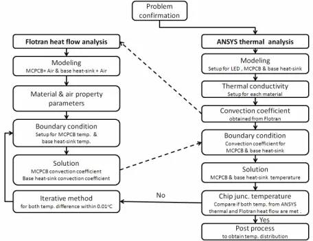
2.3. Iterative Method of Thermal Analysis
Considering the heat dissipation for convection heat transfer only, t
setup for ANSYS thermal analyses. It is very im for the settings of boundary condition since its infl on chip temperature shown the coefficient is a function of temperature and location, therefore, the result will be lack of accuracy if only input a fixed value. Based on the above reasons, the iterative method for correction of convection coefficient is proposed in this study like Fig- ure 2 analysis flowchart, which is controlled in accuracy
and reliable result for convergence. When applying Flo- tran heat flow analysis the modeling of heat dissipation components are built based on the defined ambient vo- lume to first obtain the coarse distribution of convention coefficient, accordingly the average value of surrounding component surfaces can be achieved after iterative me- thod and conduct the average thermal convention of each component surface for ANSYS boundary conditions set- up. Thus, the temperature distribution obtained from whole LED device substitutes the cooling component temperature from prior distribution plot into Flotran heat flow analysis. Repeat the above processes till the tem- perature differences within 0.01˚C for achieving con- vergence.
2.4. Response Surface Method
Response surface method (RSM) is a useful methodology for optimizat
matical analysis and statistical tech bines experimental design with re
implement systematically the experiments within the defined area. After collecting the required response val- ues, the regression analyses are conducted to collate the relations between response values and parameters for
[image:3.595.310.538.532.708.2]optimal solution found within the planned experiments. RSM combines both techniques regarding design of ex- periments (DoE) and fitting method to describe the cor- relation between design parameters with its target/re- sponse values [15]. By using RSM design optimization, the parameters can be efficiently estimated to confirm the influences with respect to target value. In this study, the Box-Behnken three-level design [16] is adopted for com- parison of both RSM methodologies.
2.5. Genetic Algorithm
Genetic algorithm (GA) was proposed by John Holland through his work [17] in the early 1970s and became popular since it has been widely experimented and ap- plied in many engineering fields that generate optimal
tance, mutation, selection, and cross-
ed to be with good ient heat dissipation, the rest of lower thermal conductive
n be ignored since . Like Figure 3 dis-
ly focused on chip,
ther- mal analysis is to determine LED power loading on and MC n in Figure 6(a), which is specified by
element type Solid70 with thermal conductivity defined solution by using techniques inspired by natural evolu- tion, such as inheri
over. GA can rapidly locate good solutions, even for large search spaces. In GA optimization, a population of strings encoded for candidate solutions are efficiently toward to optimal solution findings.
3. Modeling and Simulation
This study is based on the high power LED work lamp for product design optimization. The LED modules as connected to base heat-sink are requir
thermal conductors for effic components are composed
materials. In this study, the four LED with MCPCB and base heat-sink are modeled for thermal analysis verifica- tion because the above key components are critical for product design like Figure 1 shown the schematic.
3.1. Thermal Analysis for a Single LED with MCPCB
There is less heat directly dissipates via external case and lens for thermal conduction of single LED and MCPCB, therefore, the thermal simulation ca
limited influences on analysis result play the thermal analyses are main
chip adhesion layer (silver glue), cooling block and ther- mal paste. The dimension of LED with thermal conduc- tivity for each component is respectively specified in
Figure 4 and Table 1(a) [8,10]. The MCPCB composed
of aluminum, dielectric and copper layer with thermal conductivity for each component are respectively speci- fied in Figure 5 and Table 1(b), where the vertical
equivalent thermal conductivity is 1.5 W/m·˚C [18]. First of all, the verification process for ANSYS
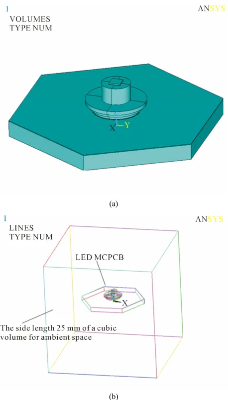
MCPCB, the simulation model setup for single LED PCB is show
LED
heat-sink MCPCB
Figure 3. Four LED with MCPCB assembled to a base heat- sink.
Figure 4. Modeling and dimension of LED components.
Figure 5. Modeling and dimension of MCPCB substrate.
in -
esh type with boundary conditions and apply 0.775 W power loading for LED device operating under 25˚C am- bient temperature.
Secondly, the boundary condition was setup for natu-
Table 1 for each component. Then, define the auto
(a)
[image:5.595.58.287.80.482.2](b)
Figure 6. Simulation of a single LED with MCPCB under ambient space.
ral convection specified by the contacting surfaces of ambient air and cooling co nent, in which the value is a function of temperature and position. The AN- SYS/Flotran heat flow analysis is used in this study which aims to avoid only one fixed-input caused inaccu- rate result and attain the convection value from surfaces of cooling components. As shown in Figure 6(b), Flor-
tan heat flow simulation model is designed for a single LED and MCPCB under ambient space. Specify element type Fluid142, setup thermal conductivity and flow pa- rameters for LED, MCPCB, and select Flotran Air-SI option in kg-m-s unit system and apply auto-mesh type for modeling mesh analysis. To facilitate analysis for boundary condition of cooling components, the initial temperature 80˚C is setup for MCPCB. After Flotran solution, an initial natural convection value for MCPCB surface is obtained. The Table 2(a) indicates the average
heat convection value summed up from each node of mpo
Table 1. Material property of LED and MCPCB. (a) LED; (b) MCPCB.
(a)
Material Thermal conductivity (W/m·˚C)
Chip (InGaN)
150
Chip adhesion layer 2
Cooling block
350 Thermal paste (T1079)
0.7
(b)
Material Thermal conductivity (W/m·˚C)
Copper
385 Dielectric layer
0.3 Aluminum
150
Equivalent thermal conductivity 1.5
MCPCB surface were initially obtained for top surface 13.71 W/m2·˚C, bottom surface 7.12 W/m2·˚C and side
surface 29.85 W/m2·˚C. Furthermore, setup the initial con-
vection v r boundary condition of ANSYS thermal
analys , ta of tem se-
quen The initial MCPC perature 80˚C from ary condition resu in 100.793˚C af l analysis, whic ows the differ- ence ˚C after first iteratio hen, return to F boundary tempe a to 100.793˚C. After iterativ s, the second convection result was collected for top surfac .82 W/m2·˚C, bottom sur-
face 7.47W 2 and side surface 31.63 W/m2·˚C re-
spectively. Average the conv
ANSYS , the MCPCB tempe 96.046˚C is obtain d ly, repeat the abov rocesses till temperat within 0.01˚C (reach to 0.004˚C after six which obtain the co v n value for
t 2 m surf W/m2·˚C
nd side surface 31.302 W/m2·˚C. Based on ANSYS
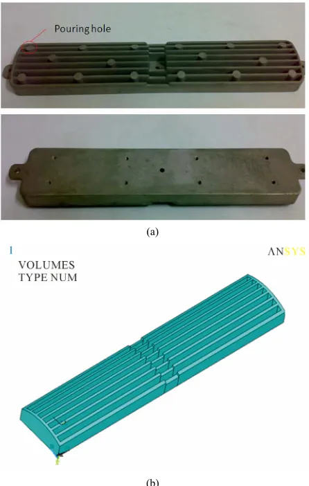
Figure 7(a) shows the base heat-sink made of ADC12
alue fo
is the da perature distribution is sub tly collected. B tem
Flotran bound ter ANSYS therma
lts h sh
up to 20.793 n. T
lotran and update its e solution
r ture
e 14 /m ·˚C
ection value and setup into
boundary rature
e . According ure difference
e p
iterations) n ectio op surface 14.605 W/m ·˚C, botto ace 7.405 a
boundary conditions, to input the confirmed convection value for top, bottom and side surfaces, and the chip junction temperature was obtained by 116.733˚C for the thermal paste 104.995˚C. Therefore, the thermal resis- tance can be achieved by Rj−s= (116.733 − 104.995)/0.775 = 15.203˚C/W, which is coincident with Everlight® LED
product specification. Similarly, adopt the same method to verify the four LED high power device and compare the iteration result for both methods.
[image:5.595.310.539.115.321.2]aluminum with thermal conductivity 92 W/m2·˚C for the
high power LED device, the simplified model in Figure 7(b) has ignored the round plastic pinholes due to its
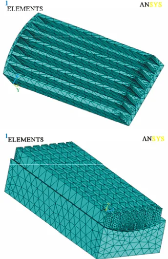
small influence but cause modeling complexity. Fur- thermore, align the four LED with MCPCB and connect to base heat-sink, the MCPCB performed a good thermal conductor for pathway without heat dissipation. Hence, construct the simulation model for single factor analysis to realize the influences of MCPCB thermal conductivity on chip junction temperature. In this study, specify ele- ment type Solid70 and thermal conductivity for each component, define the vertical equivalent thermal con- ductivity for MCPCB by 1.5 W/m2·˚C, apply manual mesh
on the critical MCPCB area and auto-mesh on remaining less influential heat-sink area, the modeling is shown in
Figure 8. Define boundary condition, ambient tempera-
ture 25˚C and power loading 0.775 W for each chip. Secondly, by means of Flotran iterative method to ob-
. As s duct modeling for this tain the convection value of ambient contacting surfaces
hown in Figure 9, the half pro
[image:6.595.313.536.84.435.2]symmetric base heat-sink was setup since its middle area not directly contact with external air. Therefore, select Air-SI option as ambient air property, define element type Fluid42 and specify thermal conductivity with auto-
Table 2. Iteration of convection coefficient for LED model. (a) Single LED model; (b) Four LED model.
(a)
Flotran heat flow analysis ANSYS thermal analysis
Convection (W/m2·˚C) MCPCBTemp. (˚C)
Iteration
Side Bottom Top Iteration
Initial 80˚C
1 29.85 7.12 13.71 1 100.793
2 31.63 7.47 14.82 2 96.046
3 31.26 7.4 14.58 3 96.997
4 31.306 7.405 14.607 4 96.893
5 31.3 7.405 14.604 5 96.904
End 31.302 7.405 14.605 End 96.9
(b)
Flotran heat flow analysis ANSYS thermal analysis
Convection Base heat-sink Chip junction
(W/m2·˚C) Temp. (˚C) Temp. (˚C)
Iteration
Side Bottom Iteration
Initial 50˚C -
1 2.86 3.64 1 52.133 90.068
2 2.87 3.65 2 52.110 90.049
(a)
[image:6.595.55.287.417.741.2](b)
Figure 7. Physical structure for base heat-sink with the sim- plified modeling.
Figure 8. Modeling of mesh layout for the four LED with MCPCB assembled to a base heat-sink.
mesh type, the model is shown in Figure 10. For the sake
of convenient calculation, the initial boundary condition for base heat-sink temperature is defined by 50˚C then the natural convection of air coefficient is conducted af- ter solution. Separate the ambient contacting surfaces into bottom and side convection area, the average convection values for each node summed up are shown in Table 2(b)
which obtain bottom surface 2.86 W/m2·˚C and side sur-
face 3.64 W/m2·˚C.
Furthermore, specify the convection values into boun-
[image:6.595.310.540.479.578.2]Figure 9. Modeling of base heat-sink with ambient space.
Figure 10. Modeling of mesh layout for base heat-sink (top) with ambient space (bottom).
dary condition, the ambient air contacting surfaces at base heat-sink bottom as well as side area are individu- ally setup for ANSYS thermal analysis. The initial tem- perature distribution for whole structure composed of four LED, MCPCB and base heat-sink are obtained. Re-
peat the above iterative calculations until temperature difference within 0.01˚C and finally reduced to 0.008˚C after three iterations, the bottom convection 2.87 W/m2·˚C
and side convection 3.64 W/m2˚C were determined as
shown in Figure 11. Finally, the chip junction tempera-
ture was confirmed by 90.053˚C to calculate the thermal resistance Rj−a = (90.053 − 25)/3.1 = 20.98˚C/W under ambient 25˚C.
4. Experiment Setup
4.1. Experiment of Thermal Resistance for High Power LED
To confirm the accuracy for high power LED simulation, the temperature calibration is first required to setup be- fore thermal resistance measurement. The experiments established for thermal measurement are respectively based on the model of single LED, four LED, MCPCB and base heat-sink, which are under natural convection environment.
1) Specification for thermal resistance measurement. The experiment setup and measurement follo nter-
test board SEMI G42-0996/ DEC 51.
le LED with MCPCB, four LED with were subsequently placed in tunnel, then applied power loading 3.1 W on each chip. From corresponding curves
w i national standards: Test method SEMI-G38-0996/SEMI G43-87/JEDEC 51, Thermal
JE
2) Process steps of thermal resistance measurement. The thermocouple made by K-Type wires was welded by hydrogen-oxygen welding machine. The temperature cor-rection was performed as follows: Fix the K-type ther- mocouple wires on the chip and place in the tempera- ture-controlled adiabatic oven. Adjust oven temperature within defined range of this experiment, the temperature output signals were collected by data capture device and kept for chip temperature in a stable condition. Then, setup three-dimensional closed test box, which was made of low thermal conductivity balsa wood in the size of 40 × 40 × 40 cm and placed it under natural convection. The device of sing
MCPCB and base heat-sink the test box and under wind
[image:7.595.315.535.598.718.2]of temperature-voltage or temperature-resistance mea- sured by sensors, the wall temperature with heat transfer
ca i-
3) Wait about half-hour to ake temperature of inter- nal heating furnace reach to steady state, record the chip and room temperature.
4) Input temperature signal into TSP curve to obtain the junction temperature then substitute into equation to calculate its thermal resistance.
5) Respectively measure four sets of data and collate results as shown in Table 3(a) summary.
6) Compare measuring data with simulation result as shown in Table 3(b). Obviously, the temperature differ-
ence between experiment and simulation is around 1%
gle factor po- CB and udy total eleven factors are
pacity were respectively obtained through data acquis tion system for signals converted to temperature, there- fore the thermal resistance can be determined.
4.2. Thermal Resistance Measurement under Natural Convection
To calculate the thermal resistance of LED package un- der a natural convection environment, the experimental data measured from TSP (Temperature Signal Processing) are setup as follows:
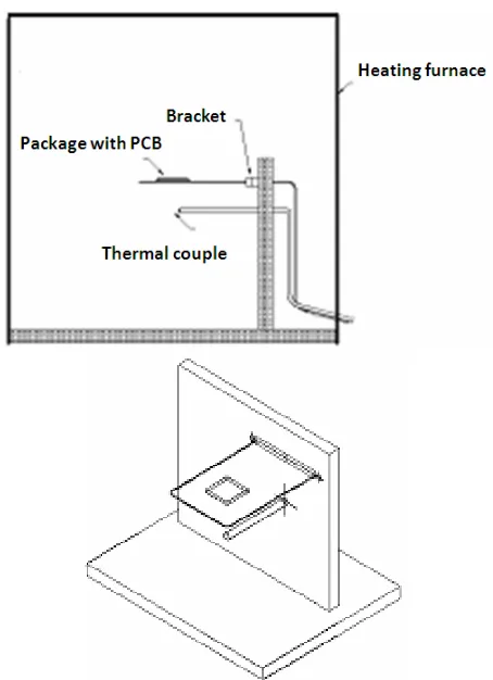
1) Utilize the characteristics of thermal resistance chip, put the supporting frame with test board into the heating furnace (initially not set any power loading) and place them in a confined space as shown in Figure 12.
2) Impose appropriate power loading on chips that is a product of voltage and current.
m
, which confirms this analysis is credible.
5. Optimization and Discussion
5.1. Analysis of Single Factor
To review each factor influences regarding to the chip junction temperature of LED device, the sin
analysis is first adopted for verification of major com nents: InGaN chip, cooling-block, thermal paste, MCP
base heat-sink. In this st
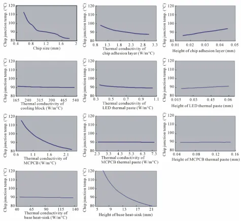
specified by different design level for baseline upper and lower 20%, 30%, 40%, 50%, respectively. Where, Level 5 is defined as baseline for changes of dimension and thermal conductivity. Keep remaining factors in the same boundary condition, the influences of each factor are shown in Figure 13 and reviewed as follows:
1) InGaN chip size: when enlarging the chip size under the same power loading, the heat dissipation per unit vo- lume will become smaller with chip junction tempera- ture reduced, whereas the smaller chip size in rising of temperature causes heating effect evidently.
[image:8.595.311.538.80.393.2]2) Thermal conductivity of chip adhesion layer (silver glue): when increasing the thermal conductivity of chip adhesion layer, the chip junction temperature will be re- duced because of the larger heat dissipation, in which the
[image:8.595.308.539.447.560.2]Figure 12. Schematic diagram of natural convection ex- periment.
Table 3. Thermal resistance under natural convection
V = 0 m/s #1 #2 #3 #4 Average
Ambient Temp.
T(˚C) 25.45 26.02 25.08 24.82 25.34
Junction Temp. Tj
(˚C) 91.08 91.86 90.66 90.42 91.01
Power (W) 3.1 3.1 3.1 3.1 3.1
Thermal Resistance Rj−a (˚C/W)
21.17 21.24 21.15 21.16 21.18
level 9 of 50% higher than baseline simply decreases 2.98% of chip junction temperature.
3) Thickness of chip adhesion layer: the chip junction temperature will be reduced because of shortening heat dissipation channel while decreasing the thickness of chip adhesion layer. Where, the level 1 of 50% less than baseline apparently decreases 4.46% of chip junction tem- perature.
Figure 13. Single factor analysis for LED package design.
5) Thermal conductivity of LED thermal paste: when increasing the thermal conductivity of LED thermal paste, the chip junction temperature will be reduced due to lar- ger heat dissipation. Where, the level 9 of 50% higher than baseline slightly decreases 1.04% of chip junction temperature.
6) Thickness of LED thermal paste: When decreasing the thickness of LED thermal paste, the chip junction temperature will be reduced due to the shortening of heat dissipation channel. Where, the level 1 of 50% less than baseline slightly decreases 1.51% of chip junction tem- perature.
7) Thermal conductivity of MCPCB substrate: when increasing the thermal conductivity of MCPCB substrate, the chip junction temperature will be reduced due to lar-
ger heat dissipation. Where, the level 9 of 50% higher than baseline significantly decreases 9.24% of chip junc- tion temperature.
8) Thermal conductivity of MCPCB thermal paste: when increasing the thermal conductivity of MCPCB thermal paste, the chip junction temperature will be re- duced due to increasing of heat dissipation. Where, the level 9 of 50% higher than baseline slightly decreases 0.11% of chip junction temperature.
10) Thermal conductivity of base heat-sink: when in- creasing the thermal conductivity of base heat-sink, the chip junction temperature will be reduced due to larger heat dissipation. Where, the level 9% of 50% higher than baseline decreases only 0.22% chip junction temperature with small effect.
11) Height of base heat-sink: when increasing the height of base heat-sink, the chip junction temperature will be reduced due to component with extended cooling area. Where, the level 9% of 50% higher than baseline evi- dently decreases 10.54% of chip junction temperature.
Review the above comparisons which confirm their design constraints, for simplification purpose all control factors were re-arranged by three-level design. Where, level 2% is setup as baseline and indicated by setting (0). Level 1 is defined by setting (−1) which respectively re- present 80% and 50% for baseline of geometric and ma- terial factors. Level 3 is defined by setting (+1) which represent 120% and 150% for baseline, respectively. The new factor design is specified in Table 4 for subsequent
analysis.
5.2. Optimization of the Response Surface Method
To verify the optimal design of the products at the lowest chip junction temperature, the fractional factorial design is first adopted for screening insignificant factor. Se- condly, the dual response surfaces as individually created by geometric and material factors are investigated. Fur- thermore, to setup the mixed response surface consider- ing factors co-existed coupling effects, the genetic algo- rithm is adopted to optimize the fitness function targeted for lowering chip junction temperature, the comparison results are conducted as follows.
5.2.1. Fractional Factorial Design
To accurately determine the significance for each factor, through fractional factorial design [16] the experimental setting should reach resolution
xperiments (2(5−1) = 16) are required for five geometric
fa
then applied quarter fractional factorial de
s are arranged by orthogonal array, and the la
[image:10.595.308.540.117.448.2]that is: D = A × B; E = A × C. For material factors, the
Table 4. Three-level design for geometric factor and mate- rial factor. (a) Geometric factors; (b) Material factors.
(a)
Factor Geometric parameter Level 1 (−1) Level 2 (0) Level 3 (+1)
A InGaN chip size (mm) 0.96 1.2 1.44
B Thickness of chip adhesion layer (mm) 0.024 0.03 0.036
C Thickness of LED thermal paste (mm) 0.032 0.04 0.048
D Thickness of MCPCB thermal paste (mm) 0.08 0.1 0.12
E Height of base heat-sink (mm) 11.528 14.41 17.292
(b)
Factor Material parameter Level 1 (−1) Level 2 (0) Level 3 (+1)
F Thermal conductivity of chip adhesion layer (W/m2·˚C) 1 2 3
G Thermal conductivity of cooling block (W/m2·˚C) 175 350 525
H Thermal conductivity of LED thermal paste (W/m2·˚C) 0.35 0.7 1.05
I Thermal conductivity of MCPCB substrate (W/m2·˚C) 0.75 1.5 2.25
J Thermal conductivity of MCPCB thermal paste (W/m2·˚C) 2.5 5 7.5
K Thermal conductivity of base heat-sink (W/m2·˚C) 46 92 138
first four factors are also arranged by orthogonal array and then the latter two items are specified by a product of three factors, that is: J = F × G × H; K = G × H × I. Ac- cordingly, applying the iterative methods by ANSYS thermal analyses, the chip junction temperature can be obtained.
1) Screening of geometric factors:
ance (ANOVA) to verify geo- F-value of factor C and D as level IV, so total sixteen
e
ctors. However, this sixteen experiments layout also can meet resolution level V, based on initial screening purpose it is therefore determined by resolution level III since enough to screen out insignificant factor. Accord- ingly, the resolution level III is setup for geometric factor screening and
sign by eight (2(5−2) = 8) experiments. In the same
method, six material factors are also processed by using quarter fractional factorial design which total require sixteen (2(6−2) = 16) experiments. In this experimental
design for geometric factors, the levels of first three con- trol factor
tter two items are specified by a product of two factors,
By using analysis of vari metric factor influences, the
shown in Table 5(a) are significantly lower than factor A,
B and E. Therefore, factor A, B and E are recognized as the significant control factors and then ignore factor C and D.
2) Screening of material factors:
Similarly, Table 5(b) shows the ANOVA to verify
material factor influences with respect to chip junction temperature and the F-value of factor G, H, J and K are evidently lower than factor F and I, so factor F and I can be identified as significant ones for subsequent analysis.
5.2.2. Design Optimization for the Dual Response Surface Method
Table 5. ANOVA of geometric and material control factors. (a) Analysis of geometric factors; (b) Analysis of material factors.
(a) Geometric
Factor S.S. DOF Square Mean F-value p-value
A 79.39 1 79.39 3.970E+7 <0.0001
B 32.03 1 32.03 1.602E+7 <0.0001
C 2.33 1 2.33 1.167E+6 <0.0001
D 0.049 1 0.049 24649 <0.0001
E 292.84 1 292.84 1.464E 8 <0.0001
Error 4.0E−6 2 2.0E−6
Total 406.65 7
(b) Material
Factor S.S. DOF
Mean
Square F-value p-value
F 455.2 1 455.2 517.6 <0.0001
G 1.5 1 1.5 1.71 0.2233
H 38.61 1 38.61 43.91 <0.0001
0001
E−3 1 9.604E−3 0.011 0.9191
I 4504.02 1 4504.02 5121.4 <0.
J 9.604
K 9.78 1 9.78 11.12 0.0087
Error 7.92 9 0.88
Total 5017.05 15
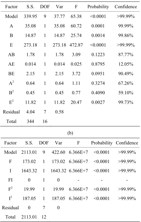
modeling, the adjusted R-Square of the geometric and material response surfaces are respectively confirmed by 0.9731 and 0.9999. Therefore, both quadratic regression models have been identified by high variance explanation as Table 6 shown the ANOVA result. Accordingly, to fit
dratic model, the with chip junction temperature by qua
geometric regression model can be expressed as follows:
2 2 2
Chip junction temperature C
126.687 22.681A 852.438B 6.467E 463.715AB 0.086AE 42.389BE 6.771A 9034.722B 0.202E
(6)
The material regression model can be expressed be- low:
2 2
Chip junction temperature C 177.57 16.13F 65.957I 2.69F 14.63I
(7)
[image:11.595.307.540.132.497.2]The geometric and material response surfaces are in-
Table 6. ANOVA of the dual response surface method. (a) Analysis of geometric response surface; (b) Analysis of ma- terial response surface.
(a)
Factor S.S. DOF Var F Probability Confidence
Model 339.95 9 37.77 65.38 <0.0001 >99.99%
A 35.08 1 35.08 60.72 99.
25.74 99.
E 87 0001 >99.
AB 0.1223 87.77%
AE 0.014 0.014 0.025 12.
90.
A2 0.64 1 0.64 1.11 0.3274 67.26%
2 0.45 45 0.77 59.
E2 7 2 9
Residual 4.04 7 0.58
Total 344 16
0.0001 0.0014
99% 86%
B 14.87 1 14.87
273.18 1 273.18 472. <0. 99%
1.78 1 1.78 3.09
1 0.8795 05%
BE 2.15 1 2.15 3.72 0.0951 49%
B 1 0. 0.4090 10%
11.82 1 11.82 20.4 0.00 7 9.73%
(b)
tor Probability d e
Fac S.S. DOF Var F Confi enc
Model 2113.01 9 422.60 6.366E+7 <0.0001 >99.99%
F 173.0 6.366E+7 >99.
7 001
FI 0 - -
2 19. 366E+7 001
2 7 >99.
Residual tal 211
2 1 173.02 <0.0001 99%
I 1643.32 1 1643.32 6.366E+ <0.0 >99.99%
1 0 -
99 1 19.99 6.
F <0.0 >99.99%
I 187.05 1 187.05 6.366E+ <0.0001 99%
0 7 0
3.01 12 To
dividually optimized by genetic algorithm for optimal so- lution, accordingly combine both optimum values for lowering chip junction temperature targeted for the- smaller-the-better, the fitness function is defined below:
Fitness function 1 objective function (8)
1) Optimization of geometric factors:
2
2 2
Fitness function
1 126.687 22.681A 852.438B 6.467E 463.715AB 0.086AE 42.389BE 6.771A 9034.722B 0.202E
(9)
Ea ned range which
out-co
ch factor is explored within defi
me is 83.3862˚C after GA optimization, as shown in
Figure 14(a). Through iterations of ANSYS thermal ana-
lysis, Table 7(a) shows the chip junction temperature is
2) Optimization of material factors:
2 2
1 177.57 16.13F 65.957I 2.69F 14.63I
Similarly, each factor is explored within defined range Fitn
(10) ess function
which outcome is 79.0532 optimization, as shown in Figure 14(b). T ugh iterations of ANSYS
th aly (b ate ip n
tem s obtained by 3˚C for 0.14% diffe- renc mpared to the tim gn iv - bine t e opti val r
factors, so-c he tim ign l e surface method, and t in oth r
thermal analysis. Table 7(c) and Figure 15(a) show the
chip nctio perature been eas
90.0 C to ˚C pr 5. th e
LED therma to 16.557˚C/ opt ion
5.2. sig z on for the Mixed Response Surface Method
Adop e quadratic model to e mixed regres-
T response surface method for GA
optimization NS ther alys G c
response surface; (b) Material response surface; (c) Dual resp e surface; (d) Mixed resp urfac
(a)
A B E .
˚C after GA hro
ermal an perature i
sis, Table 7 ) indic
79.16
s the ch junctio
e co op al desi . Respect ely com
h mum
alled t
ues f op
om geom al des
etric and m for dua
aterial respons hen put b results fo ANSYS
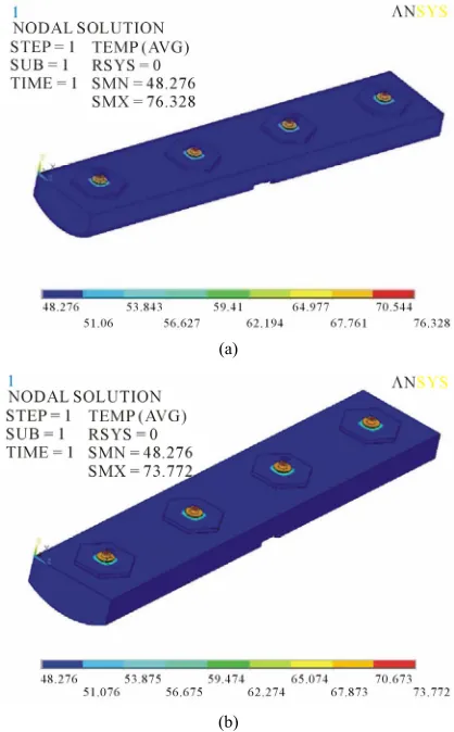
ju n tem has decr ed from 53˚ 76.328
l resistan (im
ce reduced
oving 1 24%) for e whol W after imizat .
3. De n Optimi ati
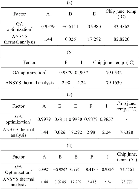
t th fit with th
able 7. Comparison of
and A YS mal an is. (a) eometri
ons onse s e.
Factor Chip junc. temp(˚C)
GA
optimization* 0.9979 −0.6111 0.9 0 98 83.3862 AN
m SYS
ther al analysis 1.44 0.026 17.292 82.8220
(b)
Factor F I Chip junc. temp. (˚C)
GA optimization* 0.9879 0.9857 79.0532
ANSYS thermal analysis 2.98 2.24 79.1630
(c)
Factor A B E F I Chip junc. temp. (˚C)
GA
optimization* 0.9979 −0.6111 0.9980 0.9879 0.9857 - ANSYS thermal
analysis 1.44 0.026 17.292 2.98 2.24 76.328
(d)
Factor A B E F I Chip junc. temp. (˚C)
GA
[image:12.595.307.539.77.638.2]Optimization* 0.9921 −0.9202 0.9954 0.4180 0.9826 73.4764 ANSYS ther
Figure 14. Chip junction temp. after GA optimization.
sion modeling, the adjusted R-Square for the mixed re- sponse surface is obtained by 0.9954. Hence, the qua- dratic regression model has been identified by high ance explanation, like Table 8 shown the ANOVA re-
sults that confirm the interactions between factor A and factor F are regarded as significant model since both
vari-
mal
analysis 1.44 0.0245 17.292 2.418 2.24 73.772
[image:12.595.56.288.411.725.2]confidence levels are greater than 99% and similar to observation in RSM contour plot. Additionally, factor B and factor F also shows the high interactive relationship. Whereas, there is no interaction between factor E and factor F, factor B and factor I, factor B and factor E by reason of their zero F-value. Accordingly, to fit with the
ch model, the mixed
regression model can be expressed as follows: ip junction temperature by quadratic
42 2
2 2 2
1 238.339 13.28A 1268.549B 6.408E 68.015F 23.467I 463.715AB 0.086AE 1.774AF 9.273AI 179.708BI 1.567 10 EF 0.429FI 1.338A 865.741B 0.152E 14.513F 2.899I
(11)
Chip junction temperature C
2 2
14.513F 2.899I
4 Fitness function
1 238.339 13.28A 1268.549B 6.408E 68.015F 23.467I 463.715AB 0.086AE 1.774AF 9.273AI 179.708BI 1.567 10 EF 0.429FI 1 (12)
2 2 2
.338A 865.741B 0.152E
90.053˚C to 73.772˚C (imp ing 18.07%), therefore the LED t al resistance has b pro t
after d optimization.
6. Conclusions
A n of t e opt the array D device is conducted as following conclusions:
1) The simulation of Flotran heat flow analysis is per- formed to mine the convection o -
tactin the natu-
ra ethod SYS
therm p ributio e four
LED, MCPCB and base t-sink have been verified with accurate result. Therefore, the chip junc perat .053˚ nd thermal resistance 20.98
identi r th from ex-
pe t 91 1˚C
a c e n h
cred sult since both re within 1%.
2) The single factor reviews conclude that the larger
chip size, thicke ase at-s th er c p layer, th er LED and MCPCB thermal pa te
bl c F e l
p vidently illustrated that the higher thermal
c p s ip cti -
ation capability.
o al design for factors
screening, the results indicate that the chip size, thickness of chip adhesion layer and height of base heat-sink are three major geometric factors. Similarly, the thermal con- ductivities for chip adhesion layer and MCPCB substrate are two major material factors. To compare both geome- tric and material major factors through F-value in ANOVA to rank their influences, it is found that the trends of re- sult are consistent with single-factor analysis.
4) To conduct both response surface methods for de- sign optimization, the results indicate that the dual RSM only need half of the mixed RSM required experimental quantity but the former cannot verify all interactions be- tween geometric and material factors. Consequentially, the mixed RSM is the most qualified method for optimal design since all factor interactions have been considered during DoE evaluations.
Through the mixed response surface method to explore each factor within defined ra e, the optimal chip junc- ng tion temperature is 73.4764˚C after GA optimization, as shown in Figure 14(c). Through iterations of ANSYS
thermal analysis, Table 7(d) and Figure 15(b) display
the chip junction temperature has been decreased from rov
herm esign
een im ved o 15.735˚C/W
n investigatio h imal design for LE
deter f ambient air con g surfaces for LED device operated under l convection. Through
al analysis, the tem
iterativ eratur
e m e dist
for AN ns of th hea
tion tem-˚C/W are ure 90 C a
fied fo rimental da e wh a, the ole pac chip ju kage. nction As measured temperature .0 nd thermal re
ible re sistan e 21.18diffe˚C/W wernces are cont obtai ed witrolled
r b he ink, inn hi
s are eligi-adhesion inn
e to reduce roperty, it is
hip junction temperature. or th materia e
onductivity su port the lowering of ch jun on tem perature due to enhanced heat dissip
3) T apply the fractional factori
(a)
(b)
Fig al
RS
[image:13.595.318.527.373.710.2]Table 8. ANOVA of the mixed response surface method.
F Probability Confidence
Factor S.S. DOF Var
Model 6004.88 20 300.24 436.83 <0.0001 >99.99%
A 100.49 1 100.49
B 52.09 1 52.09
146.2 <0.0001 >99.99%
75.79 <0.0001 >99.99%
E 602.06 1 602.06 875.96 <0.0001 >99.99%
F 482.24 1 482.24 701.62 <0.0001 >99.99%
I 4156.03 1 4156.03 6046.69 <0.0001 >99.99%
AB 1.78 1 1.78 2.59 0.1229 87.71%
AE 0.014 1 0.014 0.021 0.8868 11.32%
AF 19.81 1 19.81 28.82 <0.0001 >99.99%
AI 0.41 1 0.41 0.59 0.4502 54.98%
BE 0 1 0 0 1 0%
BF 4.65 1 4.65 6.77 0.0171 98.29%
BI 0 1 0 0 1 0%
EF 0 1 0 0 1 0%
EI 2.5E−07 1 2.50E−07
FI 0.42 1 0.42
A2 0.018 1 0.018
B2 3.008E−3 1 3.01E−03
E2 4.94 1 4.94
F2 26.03 1 26.03
I2 206.39 1 206.39 <0.0001 >99.99%
Residual 13.75 20 0.69
Total 6018.63 40
3.64E−07 0.9995 0.05%
0.6 0.446 55.40%
0.027 0.8717 12.83%
4.34E−07 0.9479 5.21%
7.19 0.0143 98.57%
37.87 <0.0001 >99.99%
300.28
5) The ANOVA results from the mixed RSM illustrate that the thermal conductivity of MCPCB and the height of base heat-sink are two of the major significant factors, the effects between chip size and thermal conductivity of chip adhesion layer are recognized as the most signify- cant interaction. For both response surface methods after GA optimization, the chip junction temperature 73.772˚C from the mixed RSM performs better than 76.328˚C from the dual RSM. The main reason is the mixed RSM has already considered all factor interactions, whereas the dual RSM not count yet. Therefore, the mixed RSM is
confirmed to be with optimal result than the dual RSM. mitting Diodes (LED) for Lighting Applications,”
7. Acknowledgements
The authors would like to express their thanks to SCI co. LTD and acknowledge the National Science Council, Taiwan, Republic of China, for financial supporting this approach under grant of NSC99-2221-E-006-038.
REFERENCES
[1] 2006. http://www.lumiled.com/technology.
[2] J. Petroski, “Thermal Challenges Facing New Generation Light E
November 2002, pp. 215-222. doi:10.1117/12.452579 [3] H. Rainer, “Thermal Management of Golden Dragon LED—
Application Note,” Osram Opto Semiconductors, Re- gensburg, 2008.
[4] J. Petroski, “Spacing of High-Brightness LEDs on Metal Substrate PCB’s for Proper Thermal Performance,” IEEE Intersociety Conference on Thermal Phenomena, Las Vegas, 1-4 June 2004, pp. 507-514.
doi:10.1109/ITHERM.2004.1318326
[5] M. Arik, C. Becker, S. Weaver, and J. Petroski, “Thermal Management of LEDs: Package to System,” Third Inter- national Conference on Solid State Lighting, San Diego, 26 January 2004, pp. 64-75. doi:10.1117/12.512731 [6] N. Narendran and Y. Gu, “Life of LED-Based White
Light Source,” IEEE/OSA Journal of Display Technology, vol. 1, No.1, 2005, pp. 167-171.
doi:10.1109/JDT.2005.852510
[7] M. Arik and S. Weaver, “Effect of Chip and Bonding De- fects on the Junction Temperatures of High-Brightness Light-Emitting Diodes,” Optical Engineering, Vol. 44, No. 11, 2005, Article ID: 111305. doi:10.1117/1.2130127 [8] C. Qian, “Thermal Management of High-Power White
LED Package,” 8 International Conference on Electronic Packaging Technology, Harbin, 14-17 August 2007, pp. 1- 5. doi:10.1109/ICEPT.2007.4441417
[9] L. Yang, J. Hu, L. Kim and M. W. Shin, “Thermal Ana- lysis of GaN-Based Light Emitting Diodes With Different Chip Sizes,” IEEE Transactions on Device and Materials Reliability, Vol. 8, No. 3, pp. 571-575.
doi:10.1109/TDMR.2008.2002357
[10] J. P. You, Y. He and F. G. Shi, “Thermal Management of High Power LEDs: Impact of Die Attach Materials,” In-
ternational Conference of Microsystems, Packaging, As- sembly and Circuits Technology, Taipei, 1-3 October 2007, pp. 239-242. doi:10.1109/IMPACT.2007.4433607 [11] P. Krivic, F.-P. Wenzl, C. Sommer, G. Langer, P. Pachler,
H. Hoschopf, P. Fulmek, J. Nicolics, “Investigation of Thermal Properties of Power LED Illumination Assem- blies,” 35 International Spring Seminar on Electronics Technology, Bad Aussee, 9-13 May 2012, pp. 76-83. doi:10.1109/ISSE.2012.6273112
[12] Y. A. Çengel, “Heat Transfer: A Practical Approach,” McGraw-Hill, Inc., Boston, 2003.
[13] Ralph Remsburg, “Thermal Design of Electronic Equip- ment,” CRC Press LLC, Boca Raton, 2001.
[14] R. H. Myers, D. C. Montgomery and C. M. Anderson- Cook, “Response Surface Methodology,” 6th Edition, John Wiley & Sons, Inc., New York, 1995.
[15] D. C. Montgomery, “Design and Analysis of Experi- ment,” 6th Edition, John Wiley & Sons, Inc., Singapore, 2005.
[16] G. E. P. Box and J. S. Hunter, “The 2k−p Fractional Fac- torial Designs Part I,” Technometrics, Vol. 42, No. 1, 2000, pp. 28-47. doi:10.2307/1271430
[17] J. H. Holland, “Adaptation in Natural and Artificial Sys- tem,” MIT Press, Cambridge, 1992.
[18] J. K. Park, H. D. Shin, Y. S. Park, S. Y. Park, K. P. Hong and B. M. Kim, “A Suggestion for High Power LED Package Based on LTCC,” Proceedings of 56th Elec- tronic Components and Technology Conference, San Die- go, 30 May 2006, pp. 1070-1075.