XRD Characterization of AlN Thin Films Prepared by
Reactive RF-Sputter Deposition
N. Matsunami1, H. Kakiuchida2, M. Sataka3, S. Okayasu3
1Energy Science Division, EcoTopia Science Institute, Nagoya University, Nagoya, Japan 2National Institute of Advanced Industrial Science and Technology (AIST), Nagoya, Japan
3Japan Atomic Energy Agency (JAEA), Tokai, Japan Email: n-matsunami@nucl.nagoya-u.ac.jp
Received January 22, 2013; revised March 10, 2013; accepted April 18, 2013
Copyright © 2013 N. Matsunami etal. This is an open access article distributed under the Creative Commons Attribution License, which permits unrestricted use, distribution, and reproduction in any medium, provided the original work is properly cited.
ABSTRACT
AlN thin films have been grown on R((1-12) surface-cut)-Al2O3, SiO2-glass and C((001) surface-cut)-Al2O3 substrates, by using a reactive-RF-sputter-deposition method. X-ray diffraction (XRD) shows that AlN film has (110) orientation of wurtzite crystal structure for R-Al2O3 and (001) orientation for SiO2-glass and C-Al2O3 substrates. The film thickness was analyzed by Rutherford backscattering spectroscopy (RBS) and it appears that XRD intensity does not show a lin- ear increase with the film thickness but a correlation with the stress, i.e., deviation of the lattice parameter of the film from that of bulk. The film composition and impurities have been analyzed by ion beam techniques. Effects of high- energy ion beams are briefly presented on atomic structure (whether stress relaxation occurs or not), surface morphol- ogy and optical properties.
Keywords: Aluminum Nitride Film; Composition; Impurities; Atomic Structure; Surface Morphology; Optical Properties
1. Introduction
It has been known that aluminum nitride (AlN) has a wide direct-bandgap (6.2 - 5.8 eV) [1,2] with hexagonal- wurtzite crystal structure [3] and unique properties: good thermal conductivity (~3 W/cmK at 300 K) [4], good insulator (>1011 Ω·cm) [5], high dielectric constant [6], relatively small linear-expansion coefficients (5.3 and 4.2 × 10⁻⁶ K−1 along a- and c-axis) [7], high sound velocity (6 km/s) [8] and large hardness [9]. Owing to these prop- erties, AlN films have potential applications to electronic devices [10], surface acoustic wave (SAW) devices [11], actuator [12], transparent hard coatings and AlN com- posites to light-emitting devices [13]. Also, AlN films have been used as buffer layer for GaN [14] and ZnO [15] film growth. For these applications, X-ray diffraction (XRD) technique have been extensively employed to evaluate the crystalline quality and growth orientation of AlN films which have been grown by various techniques, chemical-vapor atomic-layer deposition (a special type of CVD) [2], metal organic CVD [16], molecular beam epi- taxy [17], ion beam enhanced deposition (electron beam evaporation of Al combined with N ion bombardment) [5], reactive radio-frequency (RF) magnetron sputtering
deposition [6,10,18], pulsed laser deposition (PLD) [19] on various substrates, sapphire [2,19], Si [5,14-16,18], SiC [17], Al [6], Mo [12] etc. For AlN films grown on Si(111), the authors have shown that oxygen impurities near the substrate surface affect the growth orientation and suggest that the XRD intensity decreases with in- creasing the stress and nearly diminishes when the stress exceeds 2%, irrespective of the film thickness (27 - 470 nm) [20]. Here, the stress is defined as the difference of the lattice parameters between film and bulk. Use of the stress can be justified based on the fact that c-axis length increases with the residual-stress [18] and temperature dependence of the lattice parameter is similar to that of the residual-stress in terms of pressure [19]. The result does not agree with the lattice relaxation around 50 nm of AlN on SiC [17] and favors the constant stress through- out the AlN film on Si(111) [16]. It is of interest to study whether the suggested stress is useful for the quality evaluation of AlN film grown on different substrates other than Si(111).
ness and impurities, and examined use of the stress for the film quality evaluation. We also have measured sur- face morphology (grain size, shape and surface smooth-ness), which may affect the crystalline quality, since films are polycrystalline, and optical absorption. These properties might be important for applications mentioned above. For AlN on R-Al2O3, irradiation with high-energy (90 MeV Ni) ions was performed in order to study whe- ther stress relaxation, surface smoothing and bandgap modification occur or not by ion irradiation.
2. Experimental
AlN films were grown on R-Al2O3, SiO2-glass and C- Al2O3 substrates by using a reactive-RF-sputter-deposi- tion method with Al target (purity of 99.999%) in pure N2 gas of ~0.3 Pa with a method described in [20,21]. A reason for usage of pure N2 gas is to avoid Ar inclusion into films, considering that conventionally Ar and N2 mixture gas has been employed. The substrates were sub- jected to ultrasonic rinse in ethanol prior to the film deposition. XRD with Cu-kα radiation was performed to examine crystalline quality and orientation. The thick- ness, composition and impurities of films were analyzed by RBS. The growth rate was obtained to be approxi- mately 3 nm/min for AlN on three substrates used in this study. Light impurities such as carbon and oxygen near the film surface were analyzed by using nuclear reaction analysis (NRA), 12C(d, p)13C and 16O(d, α)14N with 1.2 MeV d at the reaction angle of 160˚ [20]. In RBS and NRA, stopping powers are taken after [22] with the AlN density of 3.26 g·cm−3 (4.8 × 10²² Al cm−3). Surface mor- phology was observed by atomic force microscopy (AFM) and optical absorption was measured by using a conven- tional spectrometer. Irradiation with 90 MeV Ni ions was performed by using a TANDEM accelerator at Japan Atomic Energy Agency at Tokai.
3. Results and Discussion
3.1. Characterization
Figure 1 shows XRD patterns and rocking curves of AlN film on R-Al2O3, SiO2 and C-Al2O3 substrate. The sub- strate temperature Ts was optimized, 150˚C, 200˚C and 200˚C for these substrates, respectively so that the XRD peak intensity is maximized and the full-width at half- maximum (FWHM) of XRD rocking curve is minimized. It is found that AlN film has exceptionally a-axis, i.e., (110) orientation on R-Al2O3 (diffraction angle 2θ≈ 59˚), in contrast to c-axis (2θ ≈ 36˚), i.e., (001) orientation grown on other substrates, Si, SiO2, C-Al2O3 etc. FWHM of the rocking curve of as-deposited film on R-Al2O3 is order of 2˚ (Figure 1(a) and Table 1). AlN on SiO2 glass-substrates has (001) orientation and FWHM is much larger (~10˚) (Figure 1(b) and Table 2). FWHM
0 5 10
16 17 18 19 20
X R D INT E N S ITY (a . u. )
θ (DEG.)
0 2 4 6
26 28 30 32
XR D IN TEN S IT Y (a . u .)
θ (DEG.)
0 1 2 3
30 35 40 45 50 55 60 65
XR D IN TENS ITY ( a . u.)
2θ (DEG.)
(b) AlN/SiO2 0 1 2 3 15 20 XR D I N T E NS IT Y ( a. u. )
θ (DEG.)
0 2 4 6
30 35 40 45 50 55 60 65
XR D IN TENS ITY ( a. u.)
2θ (DEG.)
(a)
AlN/R-Al2O3
0 5 10 15
30 40 50 60 70 80
XR D IN TENS ITY ( a. u. )
2θ (DEG.)
(c)
AlN/C-Al2O3
Figure 1. XRD patterns of as-deposited AlN film on R- Al2O3 (a), SiO2 (b) and C-Al2O3 (c) substrates. Rocking
curves of as-deposited films are shown in the inset and FWHM is indicated by horizontal lines. Deposition time was 55, 30 and 30 min for AlN on R-Al2O3, SiO2 (sample 70c in
Table 2) and C-Al2O3. Peaks at 2θ≈ 59˚ and 36˚ are (110)
and (002) diffraction of AlN, and 52.5˚ and 41.7˚ R- and C-plane of sapphire.
of the rocking curve of as-deposited film on C-Al2O3 is order of 0.5˚ (Figure 1(c)). Hence, the crystalline quality of AlN on SiO2-glass is poorer than that on R-Al2O3 and is the best for AlN on C-Al2O3. For AlN on C-Al2O3 used in this study, deposition time was 10 to 65 min or the film thickness ~30 to 200 nm.
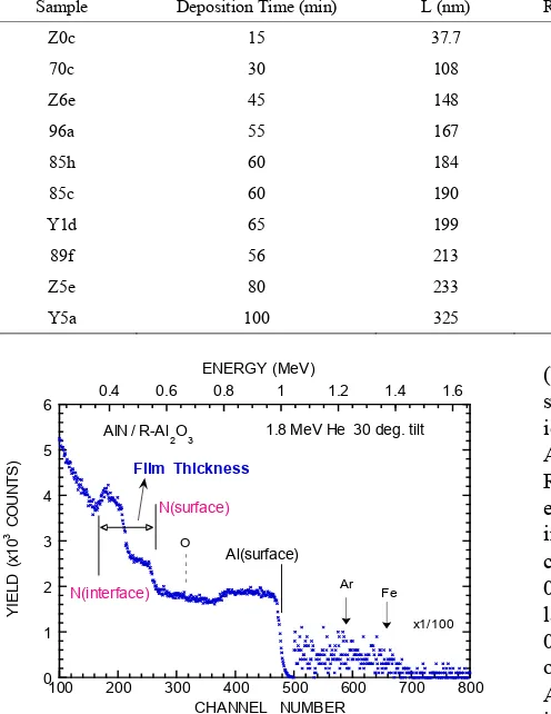
A typical RBS of AlN on R-Al2O3 is shown in Figure 2. Similar RBS spectra were obtained for AlN on SiO2 and C-Al2O3. The film thickness was deduced from the N-width illustrated in Figure 2. The thickness derived
from RBS and XRD results are summarized in Tables 1
and 2 for AlN on R-Al2O3 and SiO2. Here, accuracies of
Table 1. A summary of RBS (thickness, L) and XRD (intensity, FWHM and a-axis length) characterization of as-deposited AlN films on R-Al2O3.
Sample Deposition Time (min) L (nm) Relative Intensity FWHM (deg.) a-axis length (nm)
Z1d 15 42.7 0.85 2.68 0.3149
78b 30 95 0.002
71a 30 115 3.2 2.22 0.3157
C3d 45 148 4.4 2.14 0.3147
95c 55 171 1.0 2.81 0.3189
X6a 67 200 2.5 2.34 0.3177
98a 55 208 8.5 2.0 0.3149
X8h 100 271 5.2 2.33 0.3170
C0f 120 368 0.79 3.7 0.3214
[image:3.595.58.539.112.254.2]Y6c 160 449 10.6 2.18 0.3124
Table 2. A summary of RBS (thickness, L) and XRD (intensity, FWHM and c-axis length) characterization of as-deposited AlN films on SiO2.
Sample Deposition Time (min) L (nm) Relative Intensity FWHM (deg.) c-axis length (nm)
Z0c 15 37.7 0.01
70c 30 108 2.7 6.0 0.50764
Z6e 45 148 0.54 10 0.50887
96a 55 167 0.32 16 0.51039
85h 60 184 0.08 0.50699
85c 60 190 0.07 0.50754
Y1d 65 199 1.8 8.1 0.50685
89f 56 213 0.97 9.3 0.50936
Z5e 80 233 0.016
Y5a 100 325 2.5 8.8 0.50866
0 1 2 3 4 5 6
100 200 300 400 500 600
0.4 0.6 0.8 1 1.2
YI
EL
D
(
x1
0
3 CO
UN
T
S
)
CHANNEL NUMBE
700 800
1.4 1.6
R Al(surface)
N(interface)
N(surface)
AlN / R-Al2O3 1.8 MeV He 30
ENERGY (MeV)
deg. tilt
Film Thickness
x1/100 Fe Ar O
Figure 2. RBS of AlN on R-Al2O3 (sample 98a in Table 1).
The spectra were obtained using 1.8 MeV He, and incident and outgoing angle are 30˚ and 50˚ measured from surface normal. Energies of He scattered from Al and N located at surface andinterface are indicated by vertical lines. Ar and Fe impurities are also indicated.
thickness, XRD intensity, FWHM and axis length are estimated to be 10%, 20%, 3% and 0.3%, respectively. The composition appears to be nearly stoichiometric
[image:3.595.63.311.297.618.2]AlN on SiO2 (C: 7 to 15 × 1015 cm−2, O near the film surface: 6 to 17 × 1015 cm−2). Again no clear relation is observed between the XRD intensity and C impurity density, and between the XRD intensity and O impurity density near the film surface. The former result leads to a speculation that the majority of C impurities are located near the surface. For AlN on C-Al2O3, similar amounts of impurities are assumed.
One sees that the XRD intensity does not follow a lin- ear increase with the film thickness for AlN on R-Al2O3 and SiO2 (Tables 1 and 2) and the similar situations is observed for AlN on C-Al2O3. As suggested in [20], XRD intensity vs stress is shown in Figure 3. Here, the stress is defined by the axis length of the film divided by the bulk value (0.31111 and 0.49788 nm for a- and c-axis [23]) minus unity, assuming that the stress defined above represents the residual-stress as mentioned earlier. Usu- ally, several samples were prepared in the same run. For a particular run for AlN on R-Al2O3, having the film thickness around 380 nm, the results of four samples are shown. Accidentally, the sample (C0f) given in Table 1 is the poorest in the crystalline quality (XRD intensity is the lowest). As shown in Figure 3, it is found that the XRD intensity decreases with increasing the stress, ex- cept for the thinnest films, regardless of the substrates, as observed for AlN with c-axis orientation on Si(111) sub- strate [20]. These results indicate no relaxation of the stress regardless of the film thickness and substrates, implying that the stress is an import factor determining the crystalline quality, and that a simple explanation by misfit (lattice parameter mismatch between the film and substrate) is not applicable to the present results. Intro- duction of the stress might be affected by O, C and pos- sibly H impurities in the film as well as substrate surface condition, and these are to be investigated.
0 5 10 15
0 1 2 3 4
XR
D I
N
T
E
N
S
IT
Y
(a
u)
STRESS (%)
AlN /R-Al
2O3, SiO2 & C-Al2O3
5
Figure 3. XRD intensity vs stress for AlN films on R-Al2O3
(O, Δ, +), SiO2 (x) and C-Al2O3 (□, ●). Data (Δ) are taken for
the films prepared in the same run having the thickness of ~380 nm. Datum indicated by + is the result of the thinnest film (sample of Z1d in Table 1). For AlN on C-Al2O3, film
thickness is less than 50 nm (●) and 90 - 200 nm (□).
3.2. Surface Morphology, Optical Absorption and High-Energy Ion Irradiation Effects
Surface morphology is mainly studied for AlN on R- Al2O3 and SiO2. An AFM image of as-deposited AlN film on R-Al2O3 is shown in Figure 4(a). One sees that a column with c-axis orientation lays down parallel to the surface. The grain is often non-spherical, columnar and thus the grain size is less well-defined. It appears that the smaller size of columnar grains ranges from 20 to 40 nm and their length extends to over 250 nm, as shown in Figure 5(a) and surface smoothness (or roughness) in terms of root mean square (RMS) of the surface height ranges from 0.2 - 3 nm as shown in Figure 5(b). It ap- pears that surface roughness increases linearly with the film thickness for AlN on R-Al2O3. Figure 4(b) shows an AFM image of AlN film on R-Al2O3 after irradiation of 90 MeV Ni ions at 1 × 1013 cm−2, and ion irradiation effects will be described later. Figures 4(c) and (d) show AFM images of AlN on SiO2 and C-Al2O3 and cross sec-tion of grains on these substrates is nearly circular. The grain size of AlN on SiO2 is 10 - 40 nm (Figure 5(a)) and RMS is 0.8 - 2 nm (Figure 5(b)). Grain size is ~20 nm for AlN on C-Al2O3 shown in Figure 4(d), where RMS is 0.36 nm. In this study, surface smoothness is the best for AlN on C-Al2O3 and poorest on SiO2. For 90 MeV Ni ion irradiation on AlN on R-Al2O3 at 1013 cm−2, change was not observed in RBS (see Figure 2) and AFM image remained nearly the same as before irradiation, but sur-face roughness (RMS) slightly decreases (from 0.75 nm to 0.55 nm).
For AlN on R-Al2O3 under irradiation with 90 MeV Ni ions up to 6 × 1013 cm−2, which appears to cause signifi- cant inelastic-collision-effects [25], no change in the axis-length was observed within 0.1%, i.e., no stress re- laxation by ion irradiation and the XRD intensity at the fluence of ~6 × 1013 cm−2 decreases to half of that of as-deposited film. No appreciable but slight (several %) reduction in FWHM of the XRD rocking curve was ob- served at ~around 1013 cm−2.
Optical absorption spectra of AlN on R-Al2O3 are shown in Figure 6. The bandgap as of deposited film is obtained to be 5.7 eV in reasonable agreement with the reported value of ~6.0 eV [1,2]. Optical absorption has little changed, except for the wavelength below 300 nm (Figure 6) and the bandgap decreases by ~0.2 eV. Simi- larly, the bandgap of 5.7 eV is obtained for as-deposited AlN film on SiO2.
4. Summary
We have presented characterization of AlN films on R-Al2O3, SiO2-glass and C-Al2O3 substrates by means of XRD, ion beam technique, AFM and optical absorption. Good quality of AlN films with exceptional orientation
(a) (b)
(c) (d)
Figure 4. (a) AFM image of as-deposited AlN film on R-Al2O3. Deposition time was 55 min. Surface roughness (RMS) is 0.75
nm; (b) AFM image of AlN film on R-Al2O3 (sample shown in Figure 4(a)) after irradiation with 90 MeV Ni ions at 1 × 10¹³
cm–2; (c) AFM image of as-deposited AlN film on SiO
2 (sample: 85h in Table 2). Deposition time was 60 min. Surface rough-
ness (RMS) is 1.7 nm; (d) AFM image of as-deposited AlN film on C-Al2O3. Deposition time was 60 min. Surface roughness
(RMS) is 0.36 nm.
0 50 100 150 200
GR
A
IN
S
IZ
E
(
nm
)
0 1 2
200 250 300 350 400 450 500
AB
SO
R
B
A
N
C
E
WAVELENGTH (nm) (a)
90 MeV Ni
unir
250 AlN /R-Al
2O3 , SiO2
(a)
0 50 100 150
5 5.2 5.4 5.6 5.8 6
(ABSO
R
BAN
C
E*
E)
^2
PHOTON ENERGY (eV) (b)
90 MeV Ni
unir
0 1 2 3
0 100 200 300
RM
S
(
nm
)
FILM THICKNESS (nm)
AlN /R-Al
2O3 & SiO2
(b)
Figure 6. Optical absorption spectra before and after ir- radiation with 90 MeV Ni ions at 1 × 1013 cm–2. Inset shows
the square of absorbance times photon energy vs photon energy, illustrating bandgap determination.
400 500
Figure 5. (a) Grain size (nm) vs film thickness (nm) for AlN on R-Al2O3(O, ) and SiO◆ 2 (x) and (b) surface roughness
in terms of root mean square (RMS) vs film thickness for AlN on R-Al2O3 (O) and SiO2 (x).
irradiation with 90 MeV Ni ions have been briefly de-scribed.
5. Acknowledgements
XRD was performed at EcoTopia Science Institute and Radioisotope Research Center, Nagoya University. The authors thank Mr. T. Masuda for technical assistance of ion beam analysis performed at Nagoya University.
REFERENCES
[1] W. M. Yim, E. J. Stofko, P. J. Zanzucchi, J. I. Pankove, M. Ettenberg and S. L. Gilbert, “Epitaxially Grown AlN and Its Optical Band Gap,” Journal of Applied Physics, Vol. 44, No. 1, 1973, pp. 292-296.
doi:10.1063/1.1661876
[2] C. Ozgit, I. Donmez, M. Alevli and N. Biyikli, “Self-Li- miting Low-Temperature Growth of Crystalline AlN Thin Films by Plasma-Enhanced Atomic Layer Deposition,” Thin Solid Films, Vol. 520, 2012, pp. 2750-2755.
doi:10.1016/j.tsf.2011.11.081
[3] K. M. Taylor and C. Lenie, “Some Properties of Alumi- num Nitride,” Journal of the Electrochemical Society, Vol. 107, No. 4, 1960, pp. 308-314.
doi:10.1149/1.2427686
[4] G. A. Slack, “Nonmetallic Crystals with High Thermal Conductivity,”Journal of Physics and Chemistry of Sol- ids, Vol. 34, No. 2, 1973, pp. 321-335.
doi:10.1016/0022-3697(73)90092-9
[5] Z. An, C. Men, Z. Xu, P. K. Chu and C. Lin, “Electrical Properties of AlN Thin Films Prepared by Ion Beam En- hanced Deposition,” Surface & Coatings Technology, Vol. 196, No. 1-3, 2005, pp. 130-134.
doi:10.1016/j.surfcoat.2004.08.169
[6] X. Song, R. Fu and H. He, “Frequency Effects on the Dielectric Properties of AlN Film Deposited by Radio Frequency Reactive Magnetron Sputtering,” Microelec- tronic Engineering, Vol. 86, No. 11, 2009, pp. 2217-2221. doi:10.1016/j.mee.2009.03.036
[7] W. M. Yim and R. J. Paff, “Thermal Expansion of AlN, Sapphire, and Silicon,” Journal of Applied Physics, Vol. 45, No. 3, 1974, pp. 1456-1457. doi:10.1063/1.1663432 [8] S. P. Dodd, G. A. Saunders, M. Cankurtaran and B. James,
“Ultrasonic Study of the Elastic and Nonlinear Acoustic Properties of Ceramic Aluminum Nitride,” Journal of Materials Science, Vol. 36, No. 3, 2001, pp. 723-729. doi:10.1023/A:1004897126648
[9] I. Yonenaga, “Thermo-Mechanical Stability of Wide- Bandgap Semiconductors: High Temperature Hardness of SiC, AlN, GaN, ZnO and ZnSe,” Physica B: Condensed Matter, Vol. 308-310, 2001, pp. 1150-1152.
doi:10.1016/S0921-4526(01)00922-X
[10] A. F. Belyanin, L. L. Bouilov, V. V. Zhirnov, A. I. Kame- nev, K. A. Kovalskij and B. V. Spitsyn, “Applications of Aluminum Nitride Films for Electronic Devices,” Dia- mond and Related Materials, Vol. 8, No. 2-5, 1999, pp. 369-372. doi:10.1016/S0925-9635(98)00412-9
[11] M. B. Assouar, O. Elmazria, P. Kirsch, P. Alnot, V. Mor- tet and C. Tiusan, “High-Frequency Surface Acoustic Wave Devices Based on AlN/Diamond Layered Structure Realized Using E-Beam Lithography,” Journal of Applied Physics, Vol. 101, 2007, Article ID: 114507.
doi:10.1063/1.2739218
[12] J. Olivares, E. Iborra, M. Clement, L. Vergara, J. San- grador and A. Sanz-Hervas, “Piezoelectric Actuation of Microbridges Using AlN,” Sensors and Actuators A, Vol. 123-124, 2005, pp. 590-595.
doi:10.1016/j.sna.2005.03.066
[13] F. A. Ponce and D. P. Bour, “Nitride-Based Semiconduc- tors for Blue and Green Light-Emitting Devices,” Nature, Vol. 386, 1997, pp. 351-359. doi:10.1038/386351a0 [14] X. Ni, L. Zhu, Z. Ye, Z. Zhao, H. Tang, W. Hong and B.
Zhao, “Growth and Characterization of GaN Films on Si(111) Substrate Using High-Temperature AlN Buffer Layer,” Surface & Coatings Technology, Vol. 198, No. 1-3, 2005, pp. 350-353.
doi:10.1016/j.surfcoat.2004.10.073
[15] V. Venkatachalapathy, A. Galeckas, I.-H. Lee and A. Y. Kuznetsov, “Engineering of Nearly Strain Free ZnO Films on Si(111) by Tuning AlN Buffer Thickness,” Physica B: Condensed Matter, Vol. 407, 2012, pp. 1476-1480. doi:10.1016/j.physb.2011.09.065
[16] S. Raghavan and J. M. Redwing, “In Situ Stress Meas- urements during the MOCVD Growth of AlN Buffer Layers on (111) Si Substrates,” Journal of Crystal Growth, Vol. 261, No. 2-3, 2004, pp. 294-300.
doi:10.1016/j.jcrysgro.2003.11.020
[17] N. Onojima, J. Suda and H. Matsunami, “Lattice Relaxa-tion Process of AlN Growth on Atomically Flat 6H-SiC Substrate in Molecular Beam Epitaxy,” Journal of Crys-tal Growth, Vol. 237-239, 2002, pp. 1012-1016. doi:10.1016/S0022-0248(01)02118-2
[18] S.-H. Lee, K. H. Yoon, D.-S. Cheong and J.-K. Lee, “Re- lationship between Residual Stress and Structural Proper- ties of AlN Films Deposited by r.f. Reacrive Sputtering,” Thin Solid Films, Vol. 435, No. 1-2, 2003, pp. 193-198. doi:10.1016/S0040-6090(03)00353-5
[19] J. Keckes, S. Six, W. Tesch, R. Resel and B. Rauschen- bach, “Evaluation of Thermal and Growth Stresses in He- teroepitaxial AlN Thin Films Formed on (0001) Sapphire by Pulsed Laser Ablation,” Journal of Crystal Growth, Vol. 240, No. 1-2, 2002, pp. 80-86.
doi:10.1016/S0022-0248(02)00877-1
[20] N. Matsunami, S. Venkatachalam, M. Tazawa, H. Kakiu- chida and M. Sataka, “Ion Beam Characterization of rf- Sputter Deposited AlN Films on Si(111),” Nuclear In- struments Methods B, Vol. 266, No. 8, 2008, pp. 1522- 1526. doi:10.1016/j.nimb.2007.12.086
[21] N. Matsunami, T. Shimura, M. Tazawa, T. Kusumori, H. Kakiuchida, M. Ikeyama, Y. Chimi and M. Sataka, “Mo- difications of AlN Thin Films by Ions,” Nuclear Instru- ments Methods B, Vol. 257, No. 1-2, 2007, pp. 433-437. doi:10.1016/j.nimb.2007.01.043
[22] J. F. Ziegler, J. P. Biersack and U. Littmark, “The Stop- ping and Range of Ions in Solids,” Pergamon Press, New York, 1985.
[23] W. Martienssen and H. Warlimont, “Handbook of Con- densed Matter and Materials Data,” Springer, Berlin, 2005. doi:10.1007/3-540-30437-1
[24] J. X. Zhang, H. Cheng, Y. Z. Chen, A. Uddin, S. Yuan, S. J. Geng and S. Zhang, “Growth of AlN Films on Si(100) and Si(111) Substrates by Reactive Magnetron Sputter-
ing,” Surface Coating & Technology, Vol. 198, No. 1-3, 2005, pp. 68-73. doi:10.1016/j.surfcoat.2004.10.075 [25] N. Matsunami, M. Sataka, S. Okayasu and M. Tazawa,