Fine Pitch and Low Temperature Bonding Using Solder Bumps
and the Assessment of Solder Joint Reliability
Seung-Min Chung and Young-Ho Kim
*Division of Materials Science & Engineering, Hanyang University, Seoul, 133-791, Korea
We developed a bonding at low temperature using fine pitch Sn and In bumps at 120C, and studied the reliability of the fine pitch In-Sn solder joints. The 30mmpitch Sn and In bumps were joined together without flux at 120C for 2 minutes under 70.2 MPa. A non conductive adhesive (NCA) was applied during solder joining. Thermal cycling test (0C–100C, 2 cycles/h) of up to 2000 cycles and 1000-h temperature and humidity test (40C/95%) were carried out to evaluate the reliability of the solder joints. The bondability was evaluated by measuring the contact resistance (Rc) of the joints through the four point probe method. The solder joints were characterized by scanning electron microscopy
with energy dispersive X-ray spectroscopy. Joints between the In and Sn bumps were successfully made at 120C. The average contact resistance of the In/Sn solder joints was 10–14 mbefore thermal cycling. Without the NCA, the solder joints between the Si chip and glass substrate failed electrically in the early stages of the thermal cycling test. The failure in the solder joint during thermal cycling was attributed to the thermal expansion mismatch between the Si chip and glass substrate. In contrast, no electrical failures were observed in the joints with applied NCA even after 2000 cycles. The flip chip joints with applied NCA were stable up to 1000 hours in the temperature and humidity test. [doi:10.2320/matertrans.48.37]
(Received October 12, 2006; Accepted November 8, 2006; Published December 25, 2006)
Keywords: COG (chip on glass) bonding, NCA (non conductive adhesive) bonding, Flip chip bonding, Reliability test
1. Introduction
Electronic devices that contain heat-sensitive components require a low temperature packaging. Liquid Crystal Display (LCD) and image sensors, for example, should be processed at low temperature since the polymer materials may be degraded at high temperature.1)A low temperature bonding technique was developed using a chromium-tin-indium-gold multilayer composite,2)which is fluxless with a relatively low
bonding temperature of 140C. This technique has been applied to the Bi-Sn and In-Ag systems.3)While effective, the
above technique requires the complex multi metal layer deposition.
With the continued miniaturization of electronic compo-nents and their increasing functionality, electronics are rapidly switching towards fine pitch devices and thus the demand for these various devices has remarkably increased in recent years.4,5)The electronic devices must achieve high speed requirements and maintain excellent performance along with a higher I/O count. The flip chip technology is a viable approach that meets fine pitch and high performance requirements. A low temperature process is preferred in flip chip techniques because it minimizes the residual stresses generated by the thermal mismatch and prevents breakage or fatigue inside the device. We developed a low temperature bonding technique using In and Sn bumps.6)When the In and
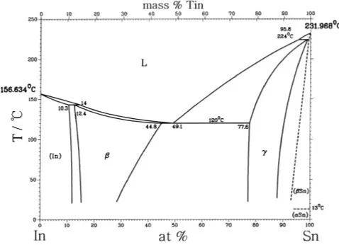
Sn solders are in contact under pressure, solder joints are formed by interdiffusion between the In and Sn solders. The interdiffusion between the In and Sn atoms leads to the formation of intermediate phases and the melting temper-ature decreases to the eutectic tempertemper-ature shown in Fig. 1.7)
Metallurgical bonding due to the melting of the intermixed phases is possible below the melting point of either pure In or Sn. Thus, solder joining is possible at temperatures lower than 150C. In this study, we investigated low temperature
and ultra fine pitch fluxless bonding using In and Sn solder bumps. The possibility of solder joint formation at 120C was investigated with 30mmpitch Sn and In bumps. Reliability tests were carried out on these fine pitch solder joints. We also applied a non conductive adhesive (NCA) to the solder joints to improve reliability.
2. Experimental Procedure
Au (0.05mm)/Cu (1mm)/Ti (0.05mm) thin films were deposited to form metal pads using DC magnetron sputtering on the Si wafer and glass substrate. The metal patterns for under bump metallurgy (UBM) and interconnection were fabricated through a photolithographic process and wet chemical etching. Solder bumps (20mm45mm) were formed on the metal pads using evaporation and the lift-off methods. The Sn solder bumps were formed on the Si wafer chips, and the In solder bumps were formed on the glass substrates.
Fig. 1 In-Sn phase diagram.7)
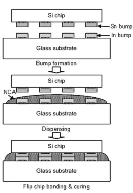
[image:1.595.306.545.349.527.2]A NCA which was composed of liquid epoxy resin and fillers (obtained from Emersion & Cuming Co. Ltd.) was dispensed on glass substrate on which the In bumps were formed using the injector and then the Sn bumps on the Si chip were aligned to the corresponding In bumps on the glass substrate using a flip chip bonder. The In bumps and Sn bumps were joined at 120C for 2 min under a pressure of 70.2 MPa which is divided the pressure (N) by the total area of the entire bumps. Figure 2 details the process flow. Solder joints were formed between the Si chip and Si substrate instead of a glass substrate to investigate the effect of differences in thermal expansion. The contact resistance was measured using the four-point probe method. Figure 3(a) represents a sketch of the test chip for the electrical tests and Fig. 3(b) shows the circuitry for contact resistance. To evaluate the bondability of the solder joints, the contact resistance of each bump was measured. To evaluate their reliability, thermal cycling test (0C–100C, 2 cycles/h) up to 2000 cycles and temperature and humidity test (40C/ 95%, 1000 h) were carried out. The initial contact resistance was measured using the four-point probe method and after each time point; the contact resistance was measured at room temperature upon completion of the thermal cycling and temperature humidity tests. The failure criterion was defined as 500 m; The value larger than 500 mwas regarded as a failed one. The failure rate means the ratio of the number of the failed solder joints to that of the total solder joints. To analyze the failure mechanism, the solder joints were cross-sectioned and characterized by scanning electron microscopy (SEM).
3. Results
3.1 Bump-to-bump bonding using 30mpitch In and Sn bumps
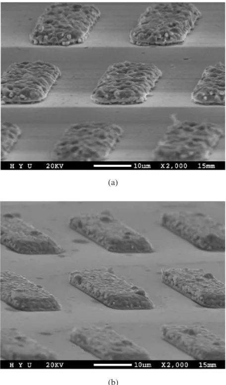
Figure 4 contains SEM images that show the In and Sn bumps of a 30mmpitch. The solder bumps were fabricated using an evaporation method and lift-off. The thickness of the In and Sn bumps was 5mmand 7.5mm, respectively. They were formed uniformly on the Au/Cu/Ti metal pads. Figure 5 shows SEM image of the Au/Cu/Ti interconnection lines and the In bumps formed on the interconnection lines for electrical testing. Figure 6 shows an SEM image of the In/Sn solder joints assembled at 120C. The bonding was successfully made through the In/Sn solder joints formed between the Si chip and glass substrate without a flux. In Fig. 6(b), the In bump on the glass substrate deformed more than the Sn bump on the Si chip after bonding because In is softer than Sn.8)
The average contact resistance of the eutectic In/Sn solder joints with and without NCA before thermal cycling are shown in Table 1. The average contact resistance values of all solder joints were measured between 10 and 14 mand no solder joints failed electrically. The contact resistance without NCA is slightly smaller than that with NCA since NCA was not trapped in the solder joint fabricated without NCA. All joints had a very low contact resistance value independent of NCA applications. The substrate type did not affect the bondability or the contact resistance of the solder joints. The contact resistances of the solder joints fabricated using the bump to bump bonding method in this experiment were much lower than that of the COG bonding using the conventional ACF method which has a few hundred mper bump.9) SEM observations and contact measurement data demonstrate that the 30-mmpitch solder bumps were joined successfully both with and without the NCA at 120C. Fig. 2 Schematic view of solder joint formation.
Glass substrate
V out
I in
V in
I out
Solder joint
(a)
(b)
[image:2.595.51.283.59.395.2] [image:2.595.313.539.69.325.2]3.2 Thermal cycling test results
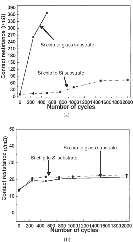
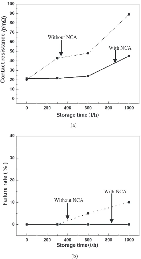
The average contact resistance of the In/Sn solder joints after thermal cycling test of up to 2000 cycles are shown in Fig. 7. The contact resistance of the solder joints bonded between the Si chip and the glass substrate without the NCA
increased quickly with increased thermal cycling and failed completely after 750 cycles. The contact resistance of the solder joints bonded between Si chip and Si substrate without the NCA increased with increasing thermal cycles and reached about 74 mafter 2000 cycles. All joints using the NCA had contact resistance values under 25 meven after 2000 cycles regardless of the substrate type. The contact resistance of the solder joints with the applied NCA increased slightly after 250 cycles and remained constant with respect to further thermal aging. The change of the contact resistance value with respect to thermal cycle in the solder joints that had NCA applied had a trend similar to the glass and Si substrates. Figure 8 shows the failure rate of the solder joints formed between the Si chip and Si substrate and between the Si chip and glass substrate without the NCA. The failure rate of the solder joints between the Si chip and glass substrate increased with thermal cycling and reached 100% after 750 cycles, but the solder joints between the Si chip and Si substrate survived up to 2000 cycles. This data suggests that reliability would be a serious problem if the NCA was not applied during the bonding between the Si chip and glass substrate.
(a)
(b)
Fig. 4 SEM images showing (a) In bumps (b) Sn bumps.
Fig. 5 SEM image showing the metal lines and In bumps.
Glass substrate
In bumpSi chip
Glass substrate
In bumpSn bump
Si chip (Sn site)
Glass substrate (In site)
(a)(b)
[image:3.595.55.283.71.459.2]Fig. 6 (a) A cross-section SEM image of the 30-mmpitch In/Sn solder joint (b) a magnified image of a solder joint in Fig. 6(a).
Table 1 The average contact resistance and deviation before thermal cycling tests with and without NCA.
Resistance [Deviation] (m)
NCA No NCA
[image:3.595.313.540.73.365.2] [image:3.595.305.549.444.499.2] [image:3.595.55.284.511.682.2]3.3 Microstructural characteristics before and after the thermal cycling tests
Figure 9 contains the back-scattered electron (BSE) image of the cross-sections of the solder joint that was bonded at 120C for 2 minutes with the NCA. The microstructure was clearly observed using the BSE image and EDX. Cu6(Sn,
In)5, AuIn2and InSn4intermetallic compounds (IMCs) were
observed in the solder joints. Most In and Sn phases transformed to InSn4 IMC and only fractions of In and Sn
phases might remain as a island form in the solder joint after bonding,9)but it was very difficult to find them. InSn
4formed
in the center of the solder joint, and Cu6(Sn, In)5 formed at
both Cu interfaces. The intermixing of the Sn and In in the solder joints indicated that interdiffusion occurred across the In/Sn interface during bonding. The Au of the UBM diffused completely into the solder to form AuIn2. AuIn2 IMCs (the
bright regions in Fig. 9) were formed as a layer along the Cu6(Sn, In)5IMCs and as an island-type in the solder center.
Figure 10 shows the BSE images of the cross-sections of the solder joints bonded using the NCA after thermal cycling. Dimensional changes and cracks in the solder joints were not found in these SEM images. One micrometer-thick Cu UBM on the chip and glass substrate were completely transformed into Cu6(Sn, In)5 after the thermal cycling test. Island-type
AuIn2IMCs were also observed. The AuIn2remained stable
at the Cu6(Sn, In)5 interface and in the center region of the
solder joint even after the thermal cycling test. The magnified images of the solder joints after the thermal cycling tests can be seen in Fig. 11. AuIn2was not uniformly distributed in the
solder joint. The large size of AuIn2 phase was observed in
some regions. But the total fraction of AuIn2 phase in the
solder joint does not seem to be increased with thermal cycling, as the low magnification pictures shown in Fig. 10. Fig. 11(a), which depicts the secondary electron (SE) image of the solder joint before thermal cycling, revealed Cu6(Sn,
In)5in the Cu interface and InSn4in the center region of the
[image:4.595.56.282.65.474.2]solder joint, which was similar to the BSE image shown in Fig. 9. As the number of thermal cycles increased, the InSn4
phase decreased and remained as an island-type phase after 500 cycles. After 750 cycles, the InSn4 phase had nearly
(r/m(r
/m
Ω
)
(r/m(r
/m
Ω
)
Si chip to Si substrate Si chip to Si substrate
Si chip to glass substrate
(a)
(b)
Si chip to glass substrate
Fig. 7 Average contact resistance of the adhesive flip chip interconnects during a 0C–100C thermal cycling test, (a) without the NCA, (b) with the NCA.
Si chip to glass substrate
Si chip to Si substrate
Fig. 8 Failure rate of the adhesive flip chip interconnects during the 0C– 100C thermal cycling test without the NCA.
4
Cu
Cu
Cu
InSn
6
(In,Sn)
5Cu
Glass substrate (In bump site)
AuIn
2Cu
6(In,Sn)
5Si chip (Sn bump site)
[image:4.595.310.541.73.258.2] [image:4.595.54.282.565.757.2]disappeared from the solder joint. In contrast, the Cu6(In,
Sn)5layer grew from the copper interfaces during the thermal
cycling test. The Cu6(In, Sn)5 layers of both interfaces
merged together after 250 cycles, and after 750 cycles most of the solder joints consisted of Cu6(In, Sn)5. The distribution
of the AuIn2 phase did not change with respect to thermal
cycling, which is consistent with the results obtained earlier (Fig. 10).
[image:5.595.54.286.73.293.2]The solder joints fabricated without the NCA are shown in Fig. 12. The solder joint consisted of Cu6(Sn, In)5, AuIn2,
and InSn4. The microstructure was similar to that of the
solder joint bonded with the NCA. Cracks formed and propagated in the Cu6(Sn, In)5 layer in the solder joint.
Cracks initiated at the surface of the solder joints and grew into the solder joints with repeated thermal cycling. The cracks were observed near the Si chip side, near the glass side, or both in the solder joints. Figure 12(c) shows that the Si chip was separated from the glass substrate as a result of cracking in the solder joint after 750 cycles.
3.4 Temperature & humidity (T & H) test results
The failure rate and the contact resistance of the solder joint with and without NCA during conditions of 40C/95% relative humidity for 1000 hours are shown in the Fig. 13. In the solder joint formed without the NCA, the failure rate and the contact resistance increased with respect to storage time. The contact resistance of the solder joints with NCA applied increased slightly after 600 h, but the failure rate remained at 0% throughout the test.
(a) 250 cycles
(b) 2000 cycles Si chip (Sn bump site)
Glass substrate (In bump site)
Si chip (Sn bump site)
Glass substrate (In bump site)
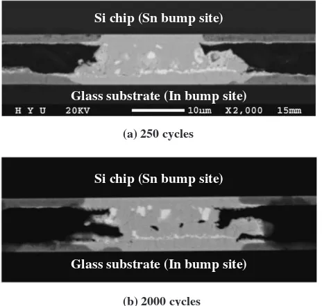
Fig. 10 Cross-sectional BS image of the In/Sn solder joint with the NCA after the thermal cycling test (a) 250 cycles (b) 2000 cycles.
(b) 250 cycles (a) 0 cycle
(c) 500 cycles (d) 750 cycles
[image:5.595.88.513.414.771.2]InSn
44. Discussion
Our results showed that the 30-mmpitch In and Sn solder bumps were joined successfully at 120C without a flux. During the bonding process, the oxide layers on the solder
surfaces prevent the In and Sn atoms from diffusing into each other, making it difficult to obtain adequate bonding.10) Therefore, a flux is normally used during the bonding process to remove the oxide layers. Since the oxide layer can be broken under high bonding pressures, interdiffusion is possible between the Sn and In solders without a flux.9)
The formation of InSn4in the solder joint proved that active
solid-state interdiffusion occurred across the interface be-tween the In and Sn bumps. As bonding continued, an intermixed layer would be formed at the interface of the In and Sn bumps. Thus, the In bump and Sn bumps can bond under temperatures below their respective melting points, namely 157C for In and 232C for Sn. All of the joints had a low contact resistance value and there were no failed joints because interdiffusion occurred irrespective of the applica-tion of NCA and regardless of substrate type.
The solder joints between the Si chip and glass substrate failed in the specimens bonded without NCA, but those between the Si chip and Si substrate survived after thermal
Cu
Cu
6(In,Sn)
5Crack
Cu
6(In,Sn)
5Si chip (Sn bump site)
Glass substrate (In bump site)
Cu
Cu
6(In,Sn)
5AuIn
22.5µ X 12000
Cu
Cu
Si chip (Sn bump site)
Glass substrate (In bump site)
AuIn
2Crack
Cu
6(In,Sn)
5Si chip (Sn bump site)
Glass substrate (In bump site)
Cu
6(In,Sn)
5Crack
(a) 250 cycles(b) 500 cycles
(c) 750 cycles m
µm
[image:6.595.52.290.68.648.2]0.5 X 10,000
Fig. 12 Cross-sectional SEM image of a crack in the In/Sn solder joint without the NCA: (a) After 250 cycling test (b) After 500 cycling test (c) After 750 cycling test.
(t/h) Without NCA
With NCA
(r/m(r
/m
Ω
)
(t/h) Without NCA
With NCA (a)
[image:6.595.313.542.70.492.2](b)
cycling. These results suggest that the failure was due to the thermal expansion mismatch between the Si and glass during the thermal cycling. The CTE of the silicon wafer is 2.7 ppm,11)and the CTE of the glass substrate used in this
experiment is measured at 10.2 ppm.12) During the thermal
cycling test, especially during the temperature dwelling period, the glass substrate expanded more than the Si wafer chip, and a thermal stress was generated. During the thermal cycling test, the Cu6(Sn, In)5 IMCs grew from the Cu
interface in the solder joints. The thickness of the Cu6(Sn,
In)5 increased with respect to increasing cycle number. As
the Cu6(Sn, In)5 comprised the major phase in the solder
joint, the solder joint became weaker since Cu6(Sn,In)5 was
harder than InSn4.9)Cracks formed in the brittle Cu6(Sn, In)5
IMC due to thermal stress. Cracks were observed in the Cu6(Sn, In)5 layer in the solder joint. The failed bumps and
cracks did not exist in the solder joints between the Si chip and Si substrate. These results indicated that the cracks formed due to the CTE mismatch between the Si and glass. In the specimen bonded with NCA, the NCA redistributed the stress and strains from the CTE mismatch and mechanical shock over the entire joint area by tightly adhering to the chip, solder joints, and substrate. As a result, crack initiation and growth in the solder joint was either prevented or drastically reduced.
It was also noticed that the contact resistance slightly increased from 0 to 250 cycles [Fig. 7(b)]. After 250 thermal cycles, Cu UBM was completely converted to Cu6(In, Sn)5
IMC which has a high resistivity (19.9m-cm).13)A slight increase in the resistance was related to microstructural changes in the solder joints.
The contact resistance of the solder joints bonded between the Si chip and glass substrates without NCA slowly increased with each test during T & H test and the solder joints began to fail after 250 hours. The increase of the contact resistance and failure rate in the solder joints without the NCA were likely due to corrosion of the interconnection lines and solder joints which were exposed to moisture during T & H test.14) The NCA suppressed the penetration of
moisture and the contact resistance did not increase rapidly in the solder joints when the NCA was applied. The secondary benefit from NCA is partial protection against moisture ingress, and other forms of contamination. Consequently, the quality and reliability of the NCA material itself will greatly impact the component reliability.15)The NCA is one of key materials in providing protection to the solder interconnect, improving mechanical integrity to the package and thereby the overall reliability of the package significantly.
5. Conclusions
In this paper, we developed a new, low temperature, fluxless bonding technique using a NCA. The reliability of the NCA-applied flip–chip joints was investigated. Without the NCA, all joints failed during the thermal cycling test. In contrast, no electrical failures were observed in the joints applied with NCA during the test. Cracks propagated through the Cu6(Sn, In)5 layer in the solder joint. The thermal
mismatch between the Si chip and the glass substrate was the main source of cracking during the thermal cycling test. The NCA improved stress distribution in the solder joints during thermal cycling and reduced the penetration of moisture during the temperature and humidity test, which markedly increased their reliability. It is believed that the In/Sn joints with NCA can be applied in low temperature, fine pitch bonding.
Acknolegement
This research was supported by a grant (F0004121-2006-22) from the Information Display R&D Center, one of the 21st Century Frontier R&D Program funded by the Ministry of Commerce, Industry and Energy of the Korean Govern-ment.
REFERENCES
1) H. Kristiansen and J. Liu: IEEE Tran. Comp. Packag. Manufact. Technol. A21(1998) 208–214.
2) C. C. Lee and S. Choe: Mater. Sci. Eng. (2002) 45–50.
3) U.-B. Kang and Y.-H. Kim: IEEE Trans. Compo. & Packag. Techno.
27(2004) 253–258.
4) U.-B. Kang and Y.-H. Kim: Int’l Sympo. On Electro. Mater. & Packag. (2001) 129–134.
5) C. C. Lee and Y.-C. Chen: Thin Solid Film.286(1996) 213–218. 6) M. S. Lee, U. B. Kang and Y.-H. Kim: Inter. Symp. Electron. Mater.
Packag. (2003) 93–97.
7) H. Okamoto:Binary alloy phase diagramsT. B. Massalski (Ed.), (ASM International, Metals Park, 1999) pp. 2295–2296.
8) E. A. Brandes and G. B. Brook: Smithells Metals Reference Book (Butterworth-Heinemann, Boston 1998).
9) S.-H. Lee and Y.-H. Kim: Key Engineering Materials 297–300 (2005) 857–862.
10) Y. C. Chen and C. C. Lee: Thin Solid Films283(1996) 243–246. 11) Y. Okada and Y. Tokumaru: J. Appl. Phys.56(1984) 314–320. 12) S.-M. Chung: Master’s Thesis (Hanyang University, Seoul 2006) 68. 13) J.-H. Choi, K.-Y. Lee, S.-W. Jun, Y.-H. Kim and T.-S. Oh: Mater.
Transac.46(2005) 1042–1046.
14) M. Datta, T. Osaka and J. W. Schultze: Microelectronic Packaging (CRC Press, New York, 2000) pp. 196.