Abstract— Vacuum electron devices are the most promising solution for the generation of watt-level power at millimeter wave and terahertz frequencies. However, the three dimensional nature of metal structures required to provide an effective interaction between an electron beam and THz signal poses significant fabrication challenges. At increasing frequency, losses present a serious detrimental effect on performance. In particular, the skin depth, on the order of one hundred nanometers or less, constrains the maximum acceptable surface roughness of the metal surfaces to be below those values. Microfabrication techniques have proven, in principle, to achieve values of surface roughness at the nanometer scale; however, the use of different metals and affordable microfabrication techniques requires further investigation for a repeatable quality of the metal surfaces. This paper compares, for the first time, the nanoscale surface roughness of metal THz waveguides realized by the main microfabrication techniques. In particular, two significant examples are considered: a 0.346 THz backward wave tube oscillator and a 0.263 THz traveling wave tube.
Keywords— BWO, surface roughness, skin depth, vacuum electron device, double corrugated waveguide, double staggered vane grating, THz vacuum electron devices
I. INTRODUCTION
acuum electron devices based on slow wave structures (SWSs) are the most promising solution for the generation of watt-level power at millimeter wave and terahertz (THz) frequencies in a compact and affordable way [1], [2], [3], [4]. A vacuum electron device (VED) consists of an electron gun to generate a collimated electron beam with high energy, an interaction structure for the interaction of the beam with a radiofrequency (RF) field, a collector to absorb the electrons at the end of the interaction structure, and a magnetic focusing field to keep the beam confined in a given
Copyright © 2015 IEEE
This work was supported in part by the UK EPSRC EP/L026597/1 grant, DARPA contract number G8U543366, NSF MRI grant CHE-1429258, DOE NSTX DE-FG02-99ER54518, DOD M67854-06-1-5118.
D. Gamzina ([email protected]), L. Himes ([email protected]), R. Barchfeld ([email protected]), B. Popovic ([email protected]), and N. C. Luhmann ([email protected]) are with the Department of Electrical and Computer Engineering at University of California, Davis; One Shields Ave, Davis CA, 95616 USA
H. Li ([email protected]), P. Pan ([email protected]), J. Feng ([email protected]) are with Beijing Vacuum Electronic Research Institute and Vacuum Electronics National Laboratory, Beijing, China
C. Paoloni ([email protected]), R. Letizia ([email protected]), M. Mineo ([email protected]) are with Lancaster University, Lancaster UK
shape. The RF generation mechanism is based on the interaction of an electron beam with a wave that propagates in a suitable waveguide, slowed down to a phase velocity close to the velocity of the electrons. The current modulation of the beam produces an aggregation of charges, namely bunches, in correspondence to the retarding front of the RF wave. The kinetic energy lost by the bunches is transferred to the field thereby determining the increase of its amplitude. The output power provided by vacuum electron devices is not achievable by solid state or photonics devices.
A broad family of vacuum electronic devices (Backward Wave Oscillators (BWOs), Travelling Wave Tubes (TWTs), klystrons, magnetrons, gyrotrons, and many others) can operate from RF to THz frequencies with power levels of mW to MW [5]. They are often the only option for many advanced technologies. For example, experimental fusion reactors employ megawatt level gyrotrons (so-called fast wave devices) for RF heating and current drive tuned to electron cyclotron or other characteristic plasma frequencies which may reach 170 GHz or beyond [6]. Plasma fusion diagnostics often operate at 100’s of GHz to pass probe beams through the reactor vessel and collect information about plasma density and temperature fluctuations [7], [8], [9]. For example, BWOs are under development to replace solid state devices and the inefficient FIR laser systems [10]. In addition, high frequency VED sources are being utilized in electron paramagnetic resonance (EPR) systems [11]. EPR is a non-destructive analytical technique to detect chemical species that have unpaired electrons. Improved spectral resolution occurs with higher frequency sources and higher magnetic fields [12]. Another example of high frequency development activity is DARPA’s ongoing Video Synthetic Aperature Radar (ViSAR) program that is utilizing advanced VEDs as an an extension of Synthetic Aperture Radar (SAR). Higher frequency radar sources provide increased image frame rate allowing for real-time image generation. The ViSAR program is utilizing high frequency (231.5 to 235 GHz), high power (50 W) VEDs [13]. VEDs have enjoyed a rich history of development and application for more than 100 years and advances continue as frequency and power requirements increase. Progress in computer technology and code development has allowed designers to build more accurate simulation models exploring advanced interaction structure designs with reduced run times and costs of development. In principle, vacuum electron devices are intrinsically scalable with frequency, but in
Nanoscale Surface Roughness Effects on THz
Vacuum Electron Device Performance
Diana Gamzina1, Hanyan Li2, Logan Himes1, Robert Barchfeld1, Branko Popovic1, Pan Pan2, Rosa Letizia3, Mauro Mineo3, Jinjun Feng2, Claudio Paoloni3, and Neville C. Luhmann Jr.1
practice, miniaturization of the vacuum devices to accommodate frequency increase has faced challenges. Fabrication technologies and electron beam current density have been the most serious limits to the development. The scaling of the periodic interaction structure can be calculated using equation (1), where φ = kz p is the phase shift within one
SWS period (kz is the longitudinal propagation constant), Vo
represents the beam voltage, and f is the operating frequency:
φ 10
( 1 )
Period values on the order of tens of microns are required for frequencies in the range of hundreds of GHz. Feature sizes of a high frequency interaction structure make its fabrication a formidable task. Three dimensional (3-D) metal structures with tolerances in the submicron range need to be realized. A handful of fabrication techniques have been used to demonstrate manufacturing feasibility of high frequency devices: photolithographic processes such as Deep X-ray LIGA (LIGA is the German acronym for lithography, electroplating, and molding), UV LIGA, and deep reactive ion etching (DRIE) on silicon, conventional milling and electric discharge machining, and state of the art nano-CNC milling via the NN100 prototype machine developed by DTL, subsidiary of DMG-Mori-Seki, available to UC Davis [14], [15], [16], [17]. Each of the manufacturing techniques has a tolerance capability associated with it as well as achievable surface roughness depending on the material used. Ensuring that the surface roughness on the walls of the manufactured interaction structure is within the skin depth at the operation frequency is essential.
For most of the metals adopted for circuit fabrication (gold, copper, aluminum), the skin depth between 100 GHz and 1 THz falls between about 200 nm and 60 nm, respectively. These nanoscale skin depth values represent an upper threshold to the surface roughness that can be tolerated without causing significant additional power losses. An estimate of the additional ohmic losses caused by surface roughness effects in the THz frequency range is fundamental for the proper modeling of the interaction structure.
II. SLOW WAVE STRUCTURES
The main frequencies of interest in the field of THz vacuum electron devices are related to the low attenuation windows of the atmosphere; in particular, they are located at 0.220 THz, 0.340 THz, 0.650 THz, and 0.85 THz [18]. While surface roughness also affects performance of fast wave structures as well as interconnects and transmission lines, this work specifically concentrates on the effects of nanoscale surface roughness on compact, lightweight, and low voltage slow wave devices. The small dimensions related to the wavelength prevent implementation of traditional structures used in VEDs such as helices or coupled cavities [5]. New concepts of topologies of the slow wave interaction structures have been developed to support waves above 100 GHz. The constraints on the dimensions and the surface roughness become more and more demanding as devices operating at frequencies spanning the “terahertz gap” [44] are desired. While surface
roughness is caused solely by the manufacturing technique, geometries of the interaction structure often play a key role in whether optimal nanoscale surface roughness quality can be achieved. In the following, three interaction structures introduced to realize THz VEDs are discussed to provide guidance in the complexity of the employed circuit geometries. Other structure types have been studied in the past (sine wave [19], coupled cavity [20], a 3D U-shaped meander-line [21], planar helix [22]), but availability of analysis of manufacturing effects on surface roughness as well as the circuit’s performance is limited.
A. Folded Waveguide
Figure 1: (a) Folded waveguide structure with a circular beam tunnel; (b) Metal fabricated folded waveguide
The folded waveguide (FWG) is an SWS which has been employed for traveling wave tubes for operation up to 0.85 THz with very wide band behavior [23]. It consists of a serpentine waveguide with a beam tunnel as shown in Figure 1 (a). High frequency communications is one of the most promising fields of applications for TWTs based on the FWG. The design of a folded waveguide is quite straightforward using analytical methods [24]. A scanning electron microscope (SEM) image of a fabricated circuit is shown in Figure 1 (b). The FWG supports a cylindrical electron beam and it is usually built in two halves. A typical tube could have a gain up to 40 dB.
B. Double Staggered Grating
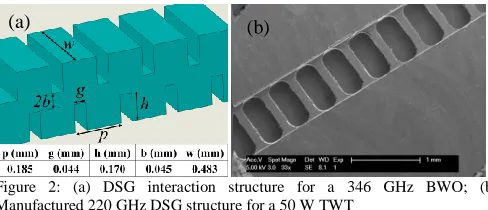
Figure 2: (a) DSG interaction structure for a 346 GHz BWO; (b) Manufactured 220 GHz DSG structure for a 50 W TWT
The Double Staggered Grating (DSG) [25] is suitable for very high output power [26]. It supports a sheet electron beam that allows propagation of a very high current carrying electron beam with reduced requirements for magnetic field strength at the beam centerline. The dimensions, the schematic, and an SEM image of a fabricated circuit for a 263 GHz structure are shown in Figure 2.
C. Double Corrugated Waveguide
The double corrugated waveguide (DCW) [27], [32] consists of two parallel rows of pillars enclosed in a rectangular waveguide which supports a cylindrical electron
(a) (b)
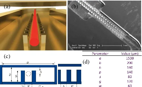
[image:2.612.314.560.195.300.2] [image:2.612.316.560.480.585.2]beam. While the use of a cylindrical beam achieves lower power compared to DSG devices, the DCW circuit’s manufacturing is simpler because it consists of complex features only on one side of the device; a sealing lid completes the vacuum envelope. The dimensions, the schematic, and an SEM image of a fabricated device are provided in Figure 3.
Figure 3: (a) Rendering of circular electron beam travelling through a DCW, (b) Manufactured 346 GHz DCW structure for a 1 W BWO; (c) DCW schematic; (d) Dimensions for a 346 GHz DCW BWO
III. ESTABLISHING SURFACE ROUGHNESS VALUE
Surface roughness is often referred to as Ra (arithmetic
mean surface roughness) or Rz (maximum height of the
roughness profile). While there are multiple standardized ways of measuring surface roughness (profiling, fringe-field capacitance, optical sectioning, light sectioning microcopy, interferometry, scanning tunneling and atomic force microscopy) [33], usually only optical techniques are the most suitable for measuring surface roughness on the walls of the high frequency interaction structure due to resolution and vertical range limitations. Confocal microscopes can be effectively used to perform a nanometer scale surface roughness measurement even a few millimeters away [34]. Surface roughness measurement is an evaluation of the local surface profile variation and is not always representative of the surface roughness across the full interaction area. To assign an appropriate surface roughness value (Ra or Rz) to a fabricated
structure, a number of measurements should be performed to obtain a statistically significant result. Measuring just three locations will provide 90% confidence level that the mean has 50% margin of error; measuring 8 locations would reduce the margin of error to 30%. Until the capability of recreating a full circuit’s nanoscale surface structure (i e by laser scanning) and measuring actual effective surface roughness value is developed for small and complex geometries, researchers have to rely on a local evaluation of the surface quality and its impact on their device performance. Attention to detail must be exercised when evaluating surface roughness so that poor as well as excellent surface roughness areas are recorded. For example, the copper surface in Figure 4 (a) and (b) has surface roughness averages of 119 nm and 245 nm, respectively; both measurements were averaged across 10 profiles in two shown locations on the scanning area of 0.188 mm x 0.141 mm. In addition, optical imaging as well as scanning electron microscopy (SEM) can be employed to gain insight into
surface quality of the device. An SEM image of a Nano-CNC machined 220 GHz TWT circuit is shown on Figure 4 (c) where high surface roughness (>1 µm) and delamination is visible on the walls. The optical microscope image of the same circuit (Figure 4 (d)) also shows clear differences between two adjacent circuit cells: left cell appears to be rougher than the right one. In addition, understanding of the EM behavior of the circuit helps in evaluating which surfaces may have higher impact on circuit’s performance It can be anticipated that, for example, the tip of the DSG structure experiences the highest electric field in operation. To achieve the best surface quality in those areas, an additional machining pass can be added at the end of circuit’s fabrication enhancing performance of the device during testing.
Figure 4: Nanoscale roughness measurement (10 profiles) of a copper surface area 188 µm by 144 µm (a) in the center of the area, (b) on the left side of the area, (c) SEM image of a 220 GHz TWT circuit, (d) optical microscope image of a 220 GHz TWT circuit
IV. LOSSES AS A FUNCTION OF SURFACE ROUGHNESS
The ability to account for the ohmic losses during the design stage of the high frequency electron device is essential for proper optimization of the design parameters to achieve the desired performance. Often, numerical simulation models of high frequency devices adopt empirical, reduced values of electrical conductivity to account for additional ohmic losses due to surface roughness.
The electromagnetic wave interacts only with the top layer of the material on the walls of the interaction structure. Finding the relationship between the effective conductivity of the top layer to use in simulation models as a function of the actual conductivity of the material and the surface roughness is not straightforward. The best procedure to determine the actual effective conductivity is to measure losses experimentally on sample structures.
Different analytical approaches were reported in the literature and described in the following [28], [29], [30], [31], [34], [35], [36]. Assuming a copper conductivity of 5.7 107 S/m and an operating frequency of 0.350 THz, an estimate of the increase of the ohmic losses as a function of surface roughness and the corresponding decrease of the conductivity is given in Figure 5 using the model in [35]. It can be noted
(a) (b)
(c)
(d) (a) (b)
[image:3.612.49.294.122.273.2]that losses double when the conductivity is reduced to a value of 1.5 107 S/m.
Figure 5: Ohmic losses as a function of surface roughness [35]
Alternatively, Eqn. (2) is used to compute additional losses caused by surface roughness (Δ is the RMS surface roughness, δ is the skin depth). This equation predicts that losses can only double as a result of poor surface roughness, due to the assumed model condition that the maximum ratio of path length on the rough surface to the smooth surface is two [35]. A more advanced version of equation (2) was developed by Lukic [36], but it has the same limitation. Lukic also evaluated losses caused by 3D surface roughness profiles, establishing that rectangular features can cause up to ~3.8 times the attenuation.
( 2 )
In summary, a discontinuity exists in the relationship between surface roughness and ohmic losses when average surface roughness value reaches value for skin depth. A more advanced model is needed to relate surface roughness structures achieved via various micro-manufacturing methods to performance modeling during design stage. For example, the electrical conductivity of the conductor had to be reduced to 1/10 of conductivity of copper to match the experimetally measured results of a 220 GHz DSG TWT circuit.
V. EFFECTS OF MANUFACTURING TECHNIQUES ON SURFACE
ROUGHNESS
The most commonly used microfabrication techniques are discussed below highlighting achievable surface quality on the walls of the manufactured interaction structure.
A. UV LIGA
KMRP or SU8 photoresist can be employed in the UV LIGA process. Figure 6 shows a summary of UV LIGA process steps. KMPR photoresist has been used in the past [37] due to its ease of removability after electroforming. However, KMPR resist is more sensitive to ultraviolet (UV) exposure dose compared to SU8 resulting in inconsistent mold quality in high aspect ratio circuit structures: delamination of the photoresist from the substrate, poor wall verticality, and poor dimensional accuracy. SU8 was chosen to micro-fabricate THz vacuum electron devices because of its excellent resolution and consistently high quality molding.
Two symmetric halves (top and bottom) are fabricated and bonded together to produce a complete FWG structure described in Section IIA. The height of the halves is only 240
µm, which requires a thickness of 300 µm of SU8 photoresist. The UV LIGA process starts with a 100 mm diameter, 10 mm thick copper wafer; a thick wafer is chosen to avoid distortion of the wafers when wire electric discharge machining of the beam tunnel of the copper FWG structure is performed. SU8 2150 [38] is dispensed on the wafer and allowed to flatten on a level hotplate, followed by a soft bake at 95°C for 120 minutes. Next, the wafer is exposed by a dose of 600 mJ UV light, followed by a post bake at 95℃. The photoresist is then developed for 15 minutes. Figure 7 (a) illustrates the SU8 mold obtained after exposure and resist development ready for electroplating.
Figure 6: Summary of UV LIGA Process: (a) exposure of thick soft baked photoresist with UV light, (b) excess photoresist is removed, (c) structure is metalized, (d) photoresist is removed producing metal cavities
The SU8 mold is copper electroformed to produce metallic microstructures. The solution used for copper plating is composed of CuSO4• H2O and H2SO4 with additives. The
deposition rate is around 10 µm/hr on the edges of wafer and about 7 µm/hr in the center. Figure 7 (b) shows an electroplated copper FWG structure. During the electroforming process, the presence of plating defects around the SU8 photoresist molds have been observed, perhaps because of variation in stir rate throughout the sample area or because of the local imbalanced ingredient ratio of the electrolyte. Figure 8 (a) shows sector areas recessed by 50 µm below the surrounding surface, Figure 8 (b) shows the ends of fingers of structures recessed by 200 µm below the surface in the worst conditions.
Figure 7: (a) SU-8 mold on the copper wafer obtained after exposure and resist development; (b) Optical microscope image of electroformed copper sample
Figure 8: Thickness defects around SU8 resist molds: (a) in the sector recessed area, (b) at the end of fingers of the structure
The electroplated structure is then immersed in Remover PG at 80℃ for several hours. During this process, the slot widths increase from 100 µm to 105 µm because the copper is slowly being etched by Remover PG during immersion. The circuits are rinsed in DI water and cleaned by a 50%
(a) (b)
(a) (b)
Sector Recessed Area
End of a Finger
[image:4.612.314.565.199.241.2] [image:4.612.315.557.444.531.2] [image:4.612.314.556.561.654.2]hydrochloric acid solution.
Copper grains produced using electroplating around SU-8 structure are 150-200 nm in size. Even though surface roughness measurements were not performed on the walls of the electroformed structures, it is estimated that obtained surface roughness is of similar scale.
B. DRIE
Deep Reactive Ion Etching (DRIE) of silicon enables microfabrication of high aspect ratio structures. It alternates an SF6 etching cycle with an S4F6 passivating cycle allowing for anisotropic etching capability essential for fabrication of high aspect ratio structures on silicon. This alternation between cycles forms scallops on the sidewalls; the surface roughness caused by scalloping can be controlled by adjusting operating parameters. Typical achievable surface roughness via DRIE is 50 to 400 nm depending on etching parameters [40].
Figure 9: (a) Resist mask of the structure on the surface of silicon wafer, (b) vertical profile of the resist
DRIE was employed to produce W (92 – 95 GHz) and G (centered around 225 GHz) band circuits. The fabrication processes of the DRIE technology are as follows: (1) Spin-coat AZ4620 photoresist with a thickness of 14 μm; (2) Softbake at 110℃ for 80 Seconds; (3) Expose resist; (4) Develop for 5 min, rinse with DI water, blow dry; (5) Etch by STS LPX ASETM; (6) remove photoresist with acetone, rinse with DI water and dry with a gentle stream of nitrogen; and (7) coat the sample with a thin copper film.
Figure 10: (a) Magnified view of prototypical W band serpentine trenches with beam tunnels (b) Cross section view of prototypical G band Clinotron HF structures
Figure 10 (a) shows SEM images of prototype W band serpentine trenches. The W band serpentine trench is approximately 946 µm deep and its sidewall profile is at 91° [39]. Figure 10 (b) shows a 220 GHz Clinotron2 high frequency structure that achieved deviation from design parameters of less than 5%, sidewall verticality of 90° [41].
2
The Clinotron operates similarly to backward wave oscillator, but the electron beam is much thicker and it is inclined with respect to the surface of the structure [42]
C. Conventional Machining
Only the most advanced commonly available machining centers that consistently achieve ~5 micron accuracy are suitable for manufacturing of structures in the high frequency regime. Achieving such tolerances using conventional machines usually depends strongly on knowledge and experience of the operator. Nanoscale surface roughness comparable to the best achieved using other advanced techniques can be obtained even on copper if machining parameters are designed for optimal conditions for individual geometry and are strictly controlled: spindle speed, feed rate, depth of cut, tool acceleration path length, tool path profile, tool shape, machine temperature, and coolant flow among many others.
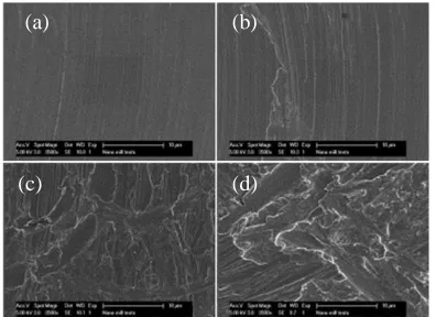
Figure 11: (a) Surface roughness (Ra) of the waveguides from left to right: 415 nm, 53 nm, 1.23 microns; (b) Surface roughness (Ra) of 74 nm, (c) Surface roughness (Ra) of 204 nm
[image:5.612.314.567.224.290.2]
Figure 12: Surface roughness identification via SEM images (a) Ra of 53 nm, (b) Ra of 159 nm, (c) Ra of 247 nm, (d) Ra of 329 nm
Optimization of these parameters was performed by machining of 0.254 mm wide channels under controlled conditions. Figure 11 (a) demonstrates that visual inspection of copper structures can provide an estimate of surface roughness. Since copper is very reflective, if there are numerous surfaces at steep angles with respect to the view of sight (very rough surface), the copper surface will appear black, whereas smooth surface will reflect the light back to the microscope thereby generating a surface image. A closer view of this phenomenon can be seen when comparing 3-dimensional recreation of the surface roughness shown on Figure 11 (b) and (c). While scanning electron microscopy (SEM) cannot be readily used to create a vertical surface roughness profile measurement, the generated SEM images can provide an insight into the quality of the surface. See Figure 12 for comparison of visible differences between surfaces with varying roughness averages.
D. Nano-CNC Machining
Nano-CNC milling has been chosen as the most suitable fabrication technique to realize circuit structures described in Section II. However, even when using advanced Nano-CNC
(a) (b)
(a) (b)
(a)
(b) (c)
(a) (b)
[image:5.612.68.279.249.336.2] [image:5.612.341.539.319.463.2] [image:5.612.52.297.472.555.2]machining techniques, careful manufacturing process planning is needed to maintain dimensional accuracy and excellent surface finish. Three distinct strategies are the key to successful fabrication of this circuit: the precision fixturing design and manufacture; the milling feeds and speeds optimized for high quality surface finish; and machining strategies that are unique to the circuit’s dimensional, material, and tooling size attributes.
The quality of the fixturing employed to hold the part is essential to achieving high tolerances and surface roughness by providing proper location identification capabilities as well as vibration isolation for the part. Finite Element Analysis (FEA) was used to predict effects on dimensional instability from allowable differences in fixture bolt tightening pressures, critical when considering that various machine setups will be used to manufacture this part. FEA model predicted that a maximum of 1.6 µm deviation will be expected on the edges of the fixturing jig.
The precision fixturing jig and the rough sized blocks for the circuits are produced on a Kitamura Mycenter 1 CNC milling machine. To achieve the highest quality surface finish, the feeds and speeds used on this CNC mill were chosen as follows: 10,000 RPM with advancement rate of < 0.001mm (1 µm) per flute RPM to attain sub-micron surface finishes. The rough machined circuit blocks securely attached to the precision fixturing jig are then transferred to the NN1000 Nano-CNC milling machine developed by DTL, a subsidiary of DMG-MORI Seiki. The NN1000 nano/micro milling machine has a maximum spindle speed of 50,000 RPM; the chip load is kept below 0.001 mm feed per tool flute RPM. This modest feed and speed strategy also reduces tool wear further assisting in achieving excellent surface finish (Ra<40
nm) and tool lifetime.
Figure 13: (a) Diamond scribing operation, (b) 220 GHz circuit fabricated using NN1000
Constant wear measurements are conducted to adjust or replace worn tools in the effort to maintain good surface finish quality and circuit dimensionality. All features are created slightly below (0.005 mm) the top plane of the circuit to allow for one final diamond tool surfacing (see Figure 13 (a)) furnishing the final part with the same quality surface finish throughout. Figure 13 (b) shows an image of a complete half of the 220 GHz TWT circuit.
E. Micro-EDM
There has been considerable interest in applying micro electric discharge (EDM) machining to fabrication of high frequency interaction structures [43], [44], [45]. While the micro-EDM process offers considerable advantages over conventional machining processes (minimal mechanical stress
on the workpiece, applicability to high aspect ratio structures), it tends to produce microscale surface roughness especially on copper structures due to the high electrical conductivity of copper. In EDM, surface roughness is caused by craters generated by the electric discharge sparks. Considerable improvements to material surface roughness manufacturing via micro-EDM have been reported by Chung [46] demonstrating 66 nm Ra on 304 stainless steel. While this
advanced method has not been used for the manufacture of high frequency interaction structures, it does provide hope for future potential if similar surface roughness values could be obtained on copper structures.
F. Molding and Printing Approaches
Molding and printing approaches are starting to see interest in the vacuum electronics community. Zhu [47] has been able to manufacture and test 3D printed metal coated plastic RF components at K-band. Frigola [48] has demonstrated 3D copper printing capabilities using electron beam melting. While neither of these technologies have capabilities for manufacturing miniature components for high frequency devices (smallest feature size is on the order of millimeters) or for producing nanoscale surface finishes yet (achievable surface finish is on the order of tens of microns), the continuous global attention on development of additive manufacturing techniques will soon provide the necessary advancements [49].
VI. POST-MANUFACTURING SURFACE ROUGHNESS
IMPROVEMENT TECHNIQUES
A. Chemical Polishing
When etching time is closely controlled, it is possible to improve nanoscale surface roughness by chemical polishing in an acid solution. Copper bright dip [50] can provide a slower and more controlled etch compared to other copper etchants. Figure 14 (a) and (b) show surface roughness before and after etching: the roughness caused by the tool marks as well as the direction change of the tool path has been significantly reduced (improvement in Ra from 300 nm to 200 nm), but size
of the imperfections in the material structure has slightly increased.
[image:6.612.63.283.450.540.2]
Figure 14: Surface roughness (a) before and (b) after etching; channel size is 0.5 mm
B. Annealing
Joye [51] has perfected SU-8 LIGA manufacturing techniques for a folded waveguide interaction structure with imbedded polymer string for beam tunnel cavity formation. Since removal of the SU-8 mold is performed in a molten salt bath that also attacks copper, post-processing of the metal structures is essential for achieving desirable surface
(a) (b)
[image:6.612.318.562.525.623.2]roughness. Joye demonstrated that annealing of produced copper structures at 1070°C in a hydrogen environment can reduce peak-to-peak surface roughness from a few microns down to a few hundreds of nanometers [52].
The copper circuits produced using KMPR UV LIGA described above were annealed at 800°C in a vacuum environment to eliminate internal stresses and improve surface roughness. The manufactured FWG copper circuit is shown in Figure 15 (a) and (b) and optical images of the walls before and after annealing are shown in Figure 15 (b) and (c). While annealing operation can significantly smooth out local non-uniformities on the surface, it also promotes grain growth affecting mechanical properties of the material.
Figure 15: Magnified view of the circuit after annealing at temperatures of 800℃: (a) optical image, (b) SEM image; (c) optical image of the
electroplated copper wall after KMPR mold removal, (d) optical image of material microstructure after annealing
C. Electro-Polishing
Electro-polishing techniques have not been commonly used on improving surface roughness of high frequency microwave structures, but they would offer a potential for reducing surface roughness to just a few tens of nanometers as they have for high gradient accelerator cavities [53], [54]. In addition to adapting the technique to microscale structures, the main challenges that would need to be overcome are the mass transfer rate of copper ions near the surface to minimize pitting and surface contamination.
VII. CONCLUSIONS
The ability to achieve nanoscale surface roughness on walls of high frequency interaction structures is essential for advancing the high frequency electronics field towards high power devices in the terahertz regime. As a part of the development of a 346 GHz BWO with applications in plasma fusion diagnostics, UC Davis, Lancaster University, and the BVERI team has investigated available manufacturing techniques and their respective capabilities in achieving nanoscale surface roughness. This work presents an essential background for achieving nanoscale surface roughness for advancing the development of high frequency devices: considerations when measuring surface roughness, surface roughness impact on RF losses, available manufacturing techniques and their limitations, and available material
post-processing techniques enhancing surface quality. VIII. REFERENCES
[1] P. H. Siegel, "Terahertz Technology," Microwave Theory and Techniques, IEEE Transactions on , vol.50, no.3, pp.910,928, Mar 2002 [2] Chattopadhyay, G “Technology, Capabilities, and Performance of Low
Power Terahertz Sources”, Terahertz Science and Tech , IEEE Trans on 2011, pp. 33- 53
[3] Korolev, S. et al., "Traditional and novel vacuum electron devices", IEEE Trans. On Electron Devices, vol.48, no.12, pp.2929-2937, Dec 2001
[4] M Mineo, C Paoloni, “Corrugated Rectangular Waveguide Tunable Backward Wave Oscillator for THz Applications”, IEEE Trans on Electron Devices, Vol.57, N.6, pp.1481-1484, June 2010
[5] J.H. Booske, et al., “Vacuum Electronic High Power Terahertz Sources”, IEEE Transactions on Terahertz Science and Technology, Vol. 1, No. 1, September 2011
[6] T Omori et al “Overview of the ITER EC H&CD system and its capabilities”, Fusion Engineering and Design, 86, pp 1-954, 2011 [7] Luhmann, Jr. N. C., et. al Chapter 3 Microwave Diagnostics,
(Invited) Special Issue of Fusion Science and Technology on MFE
Diagnostics, 2008 Fusion Sci. and Technol. 53 335
[8] John Sheffield, et al., Plasma Scattering of Electromagnetic Radiation (Second Edition): Theory and Measurement Techniques, Copyright © 2011 Elsevier Inc.
[9] D.R. Smith, et al., “A collective scattering system for measuring electron gyroscale fluctuations on the National Spherical Torus Experiment”, Review of Scientific Instruments 79, 123501, 2008.
[10] B. Popovic, at al., “ 46 GHz BWO for Fusion Plasma Diagnostics”, 39th International Conference on Infrared, Millimeter, and Terahertz Waves, Tucson, AZ, September 14-19, 2014
[11] A. Schweiger, G. Jeschke, Principles of Pulse Electron Paramagnetic Resonance (Oxford University Press, 2001)
[12] P. J. Bratt, et al., J. Phys. Chem. B 101, 9686 (1997). [ISI]
[13] H B Wallace “Video Synthetic Aperture Radar (ViSAR) DARPA” April 30, 2012
[14] Pan Pan, et al. Progress of G band folded waveguide TWT, Proceedings of IEEE International Vacuum Electronics Conference , 2015
[15] Anisullah Baig, at al., “MEMS Vacuum Electronics,” Encyclopedia of Nanotechnology 2012, pp 1359-1368
[16] Gamzina, D, et al., "Nano CNC milling technology for terahertz vacuum electronic devices," in Vacuum Electronics Conference (IVEC), 2011 IEEE International, pp.345-346, 21-24 Feb. 2011
[17] R. Barchfeld, et al., “Nano CNC milling of two different designs of 0 22 THz TWT circuits,” in Vacuum Electronics Conference (IVEC), 2012 IEEE Thirteenth International, 2012, pp. 549–550
[18] Slocum DM, et al. Atmospheric absorption of terahertz radiation and water vapor continuum effects. J Quant Spectrosc Radiat Transfer (2013), http://dx.doi.org/10.1016/j.jqsrt.2013.04.022
[19] Xiong Xu, et al., "Sine Waveguide for 0.22-THz Traveling-Wave Tube," in Electron Device Letters, IEEE , vol.32, no.8, pp.1152-1154, Aug. 2011
[20] Y. Liu, et al., "Design of a v-band high-power sheet-beam coupled-cavity traveling-wave tube," Progress In Electromagnetics Research, Vol. 123, 31-45, 2012
[21] C. Chua; Aditya, S., "A 3-D U-Shaped Meander-Line Slow-Wave Structure for Traveling-Wave-Tube Applications," in Electron Devices, IEEE Transactions on , vol.60, no.3, pp.1251-1256, March 2013 [22] C. Chua, et al., “Microfabrication and characterization of W-band planar
helix slow-wave structure with straight-edge connections”, Electron Devices, IEEE Transactions on 58 (11), 4098-4105
[23] M. Mineo, C. Paoloni, "Comparison of THz backward wave oscillators based on corrugated waveguides," Progress In Electromagnetics Research Letters, Vol. 30, 163-171, 2012.
[24] M. F. B. A. Malek, "The analytical design of a folded waveguide traveling wave tube and small signal gain analysis using madey's theorem," Progress In Electromagnetics Research, Vol. 98, 137-162, 2009.
[25] Y.-M. Shin, et al., “Strongly confined plasmonic wave propagation through an ultrawideband staggered double grating waveguide,” Applied Physics Letters, vol. 93, no. 22, p. 221504, 2008.
[26] M. Field, et al., “Deevelopment and Test of a Travelling Wave Tube mm-wave Source,” APS March Meeting, W21.001, March 2013
(a) (b)
[image:7.612.49.286.207.378.2][27] Claudio Paoloni, et al., “Design and Realization Aspects of 1-THz Cascade Backward Wave Amplifier Based on Double Corrugated Waveguide”, IEEE Trans on Electron Devices, Vol 60, March 201 , 1236 – 1243
[28] S. Lucyszyn, “Accurate CAD Modeling of Metal Conduction Losses at Terahertz Frequencies,” Electron Devices for Microwave and Optoelectronic Applications, 2003, pp.180-185.
[29] G Stupakov, K L F Bane, “Surface Impedance Formalism for a Metallic Beam Pipe with Small Corrugations,” SLAC-PUB-15231 [30] P Zhang, “Effects of Surface Roughness on Electrical Contact, RFF
Heating, and Field Enhancement,” PhD Dissertation, Nuclear Eng And Radiological Sciences, Univ. of Michigan, 2012
[31] B. Yang, et al., “Theoretical and Empirical Evaluation of Surface Roughness Effects on Conductivity in the Terahertz Regime,” IEE trans On Terahertz Science and Technology, Vol. 4, No. 3, 2014
[32] M Mineo and C Paoloni, “Double-Corrugated Rectangular Waveguide Slow-Wave Structure for Terahertz Vacuum Devices,” IEEE Transactions on Electron Devices, vol. 57, no. 11, pp. 3169–3175, Nov. 2010.
[33] T V Vorburger, J Raja, “Surface Finish Metrology Tutorial,” NISTIR 89-4088, 1990.
[34] D A Lange, H M Jennings, S P Shah, “Analysis of surface roughness using confocal microscopy,” Journal of Materials Science, 28, pp. 3879-3884, 1993.
[35] E. Hammerstad and O.Jensen, "Accurate Models for Microstrip Computer-Aided Design," Microwave symposium Digest, 1980 IEEE MTT-S International, pp.407,409, 28-30 May 1980
[36] M. V. Lukic, D. S. Filipovic, “Modeling of -D surface roughness effects with application to µ-coaxial lines,” IEEE Trans. On Microwave Theory and Technique, Vol. 55, No. 3, March 2007.
[37] H Li,Y Li,and J Feng, “Fabrication of 40GHz Folded Waveguides Using KMPR Photoresist”, Electron Device Letters, March 2013, Volume 34, pp 462-464
[38] “SU-8 2000 Permanent Epoxy Negative Photoresist,” MicroChem [39] Hanyan Li, Jinjun Feng and Guodong Bai, “Microfabrication of W-Band
Folded Waveguide Slow Wave Structure Using DRIE and UV-LIGA Technology”, IVEC2011, India, pp379-380
[40] K S Chen et al “Effect of Process Parameters on the Surface Morphology and Mechanical Performance of Slicon Structures after Deep Reactive Ion Etching (DRIE),” Journal of Microelectromechanical Systems, Vol.11, No. 3, June 2002.
[41] Hanyan Li, Dapeng Ren, Jinjun Feng, “Design and Microfabrication of 220GHz Clinotron HF Structure”, IVEC 2012, California, U S A, pp 397-398
[42] D M Vavriv, “Potential of the Clinotron for THz Generation,” High Energy Density andHigh Power RF: 7th Workshop, 2006.
[43] G. P. Scheitrum, in Modern Microwave and Millimeter-Wave Power Electronics, edited by R. J. Barker, J. H. Booske, N. C. Luhmann, and G. S. Nusinovich IEEE/Wiley, New York, 2005, Chap. 7
[44] J H Booske, “Plasma physics and related challenges of millimeter-wave-to-terahertz and high power microwave generation,” Physics of Plasmas, Vol. 15, 055502, 2008
[45] Sharma, R.K. et al. "20.6: Design and development of 100 GHz folded waveguide TWT," in Vacuum Electronics Conference (IVEC), 2010 IEEE International , vol., no., pp.505-506, 18-20 May 2010
[46] D. K. Chung, et al., “Machining characteristics on electrochemical finish combined with micro EDM using deionized water,” International Journal of Precision Engineering and Manufacturing, Vol. 15, Issue 9, pp. 1785-1791, 2014
[47] R Zhu, D Marks, “Rapid prototyping lightweight millimeter wave antenna and waveguide with copper plating,” 40th International Conference on IRMMW-THz, 2015
[48] P Frigola et al “Fabricating Copper Components with Electron Beam Melting,” Advanced Materials and Processing, July 2014
[49] A Triantaphyllou, “Surface texture measurement for Additive Manufacture,” Proceedings of ASPE Spring 2014
[50] M Baldwin, J Pope, “Stanford Synchrotron Radiation Project User Specifications for Vacuum Systems and Components which Interface with the SPEAR Vacuum System,” SLAC-TN-73-13, October 1973 [51] C. D. Joye, et al., “UV-LIGA microfabrication of 220 GHz sheet beam
amplifier gratings with SU-8 photoresist,” Journal for Micromechanics and Microengineering, Vol 20, 125016, 2010
[52] C. D. Joye et al , “Microfabrication of fine electron beam tunnels using UV-LIGA and embedded polymer monofilaments for vacuum electron
devices,” Journal for Micromechanics and Microengineering, Vol. 22, 015010, 2012
[53] A.M. Awad, et al., “Removal of tarnishing and roughness of copper surface by electropolishing treatment,” Applied Surface Science, Vol. 256, Issue 13, pp. 4370-4375, April 2010
[54] Takahata, K.; Aoki, S.; Sato, T., "Fine surface finishing method for 3-dimensional micro structures," in IEEE Proceedings on Micro Electro Mechanical Systems, pp.73-78, 1996
Diana Gamzina receiveddouble B.S. degree in Mechanical Eng. and
Materials Science in 2008, M.S. degree in Mechanical Eng. in 2012, and is completing her Ph.D. degree with focus on thermo-mechanical design and analysis of high power and high frequency vacuum electronics in 2015. She has been staff member of the UC Davis mm-wave research group since 2008.
Hanyan Li received Ph.D. degree in physical electronics from Beijing
Vacuum Electronics Research Institute in 2014. Her research interests are in Terahertz devices, microfabrication technology, and micro-electronics technology.
Logan Himes received his B.S. from UC Davis in 2010 in Biotechnology and
Applied Microbiology. Since 2010 he has worked as an Associate Development Engineer for UC Davis mm-wave research group focusing on the development of precision and high performance micro and nano-machining as well as manufacturing strategies and techniques for the production of high frequency vacuum electronics.
Robert Barchfeld is a PhD student at UC Davis, Dept, of Applied Science. Robert’s focus of study is plasma physics and fusion technology under the guidance of Professor Neville Luhmann. His primary research involves the design, construction, and implementation of plasma diagnostic instruments. He also performs research in vacuum electronics, micro-fabrication, and related millimeter wave technologies.
Branko Popovic is a PhD student at UC Davis, Dept. of Electrical and
Computer Engineering, and a member of the Davis Millimeter-Wave Research Center (DMRC) Branko’s research focus is millimeter wave vacuum electronics under the guidance of Professor Neville Luhmann with main focus on the design of vacuum electronic devices using electromagnetic and particle in cell codes. Additionally he is involved in laboratory testing of these devices and related components.
Pan Pan received the B.S. degree in engineering from Tsinghua University,
China in 2010, and the M.S. degree in physical electronics from Beijing Vacuum Electronics Research Institute, China in 2015. He joined BVERI in 2010 as an assistant engineer developing W band TWTs. Since 2013, he has been mainly responsible for designs of the slow wave structures of 220 GHz and 340 GHz TWTs.
Rosa Letizia (M’1 ) received the Ph. D. degree in computational photonics from University of Leeds, UK, in 2009. Since 2011, she joined the E-MIT group at the Engineering Department, Lancaster University, and the Cockcroft Institute, UK, to work as a Lecturer.
M. Mineo received the Ph.D. degree in telecommunication and
microelectronic engineering from the University of Rome “Tor Vergata”, Rome, Italy. Since 2012, he has been a Research Associate with the Department of Engineering, Lancaster University, Lancaster, UK
Jinjun Feng (M’94-SM’06) is the Vice Chief-Engineer of BVERI and the
Head of the Vacuum Electronics National Laboratory in China. He has authored/co-authors 1 book, 1 book Chapters and over 200 papers in domestic and oversea conference proceedings and scientific journals. He had been the Chair of IEEE EDS Beijing Chapter (2011-2012), and currently is the Chair of IEEE Beijing Section since 2014. He is a Fellow of Chinese Institute of Electronics (CIE) since 2013 and a member of IEEE EDS Vacuum Electronic Technical Committee since 2010.
Claudio Paoloni (M’86–SM’11) received the Laurea Degree in Electronic
Engineering from the University of Rome “Sapienza”, Rome, Italy, in 1 84
Since 2012, he has been a Professor of electronics with the Department of Engineering, Lancaster University, Lancaster, U.K He is Head of Engineering Department
N.C. Luhmann, Jr. received Ph.D. degree from Univ. of Maryland, College
![Figure 5: Ohmic losses as a function of surface roughness [35]](https://thumb-us.123doks.com/thumbv2/123dok_us/1059626.622272/4.612.314.556.561.654/figure-ohmic-losses-function-surface-roughness.webp)