Analysis of multiphase clocked electron pumps consisting
of single-electron transistors
Shuhei Amakawaa)
Microelectronics Research Centre, Cavendish Laboratory, Cambridge CB3 0HE, United Kingdom
Hiroshi Mizuta and Kazuo Nakazato
Hitachi Cambridge Laboratory, Cavendish Laboratory, Cambridge CB3 0HE, United Kingdom
共Received 25 October 2000; accepted for publication 30 January 2001兲
Pump circuits consisting of single-electron transistors are analyzed in which electrons are pumped by multiphase clock pulses. An optimal low-temperature operation condition is presented where pumped current is maximized, yet the power consumption is not. Approximate formulas for the number of electrons transferred per clock cycle and the power consumption are derived for that condition, which clearly show the advantage of the pump circuits for low-power applications. The power consumption becomes even less at higher temperatures. However, the relatively large island capacitance between transistors limits the operation temperature. © 2001 American Institute of
Physics. 关DOI: 10.1063/1.1358314兴
I. INTRODUCTION
The ability to control the transfer of single electrons is a distinctive feature of single-electron devices. Some of them, including the single-electron turnstile1 and the single-electron pump,2 are able to transfer electrons one by one synchronized with some clock signal. There have been some proposals for circuit construction which exploit the precision control of single electrons.3–5 In those circuits, presence or absence of a single excess electron represents a single bit.
Tsukagoshi et al. later experimentally demonstrated the operation of electron pump circuits composed of multiple tunnel junctions 共MTJs兲.6,7The MTJs were formed in side-gated␦-doped GaAs wires.8,9By applying a negative voltage to a side gate, ultrasmall islands appeared in the two-dimensional electron gas共2DEG兲layer due to randomly dis-tributed dopant atoms. In addition, within a certain range of side-gate bias voltage, the side gate also worked as a single-electron transistor gate, thereby turning an MTJ into a tran-sistor. Two types of pumps were studied by them. One con-sisted of a pair of MTJ transistors and was driven by an ac clock signal.6,10 It was also referred to as the bidirectional electron pump. The other contained three or more MTJ tran-sistors and was driven by unipolar multiphase clock pulses,7 as shown in Fig. 1. We look into the latter multiclocked pump circuit in this article.
In spite of its apparent resemblance to the ‘‘original’’ single-electron pump,2 the operation principle of Tsuka-goshi’s multiclocked pump is quite different from that of the original one. In the case of the original pump, all the capaci-tances contained in a device are of the same order. Conse-quently, it is indivisible in the sense that one has to consider the condition of Coulomb blockade taking the entire device into account. On the other hand, Tsukagoshi’s pump in-volves two different capacitance scales. One is of the capaci-tances that constitute an MTJ transistor and the other is of
the capacitances of clocking gates. The clocking-gate capaci-tances, which are situated between MTJ transistors, are con-siderably larger than other capacitances in the pump. As a result, component MTJ transistors work virtually indepen-dently of one another as if being voltage biased, and basi-cally the pump operation reflects the MTJ transistors’ I – V characteristics rather than the precise charge configuration in the circuit. In other words, Tsukagoshi’s pump is essentially a series connection of ac biased single-electron transistors.11 It implies that the pump is not very suitable for transferring precisely one electron per cycle. If one calculates the number of electrons transferred per cycle Nc from the net current I
and the clock frequency f using the relationship I⫽Nce f , Nc
is typically a few tens to several hundred. However, the pump is still a ‘‘single-electron’’ device in the sense that it utilizes Coulomb blockade of single-electron transport as will be elaborated upon later.
From a perspective of application, the multiclocked pump is potentially useful as a building block of binary de-cision diagram 共BDD兲 logic circuits.5 Some experiments have already been conducted along the lines.12,13However, the pump’s charge transport mechanism and its possible per-formance have not been well-understood yet. Among other things, power dissipation is of great interest. In the conven-tional complementary metal–oxide–semiconductor logic cir-cuits, the power of a logic gate is
P⫽f⫻q⫻Vdd, 共1兲
where q⫽CLVddis the amount of charge that flows from the dc supply line to the ground per clock cycle, Vdd is the dc supply voltage, and CL is the effective load capacitance.14
Since the pump does not have any dc bias, the common way to estimate the power is not directly applicable. The purpose of this article is to analyze the operation of the pump circuit within the semiclassical model and to evaluate the power dissipation, with the said application in mind. The next sec-tion describes the basic theory whereby we perform analysis
a兲Electronic mail: [email protected]
5001
and simulations. The simplified model used in this article is presented in Sec. III. Section IV is devoted to the analysis of the pump operation at the low temperature limit. Approxi-mate formulas for the number of electrons transferred per clock cycle and the power consumption are derived. The effect of finite temperature and the upper bound of operation frequency are treated in Sec. V. Finally, an outlook for scal-ing down and the logic circuit application is discussed in the last section.
II. ENERGY DISSIPATION AND TUNNELING
Semiclassical treatment of single-electron circuits with the global rule of Coulomb blockade is known to work rea-sonably well for application-oriented circuit analyses.15 We apply it to pump circuits consisting of tunnel junctions, ca-pacitors, voltage sources, and ideal leads. The amount of energy dissipation is what one needs to know to calculate tunneling rates and to evaluate the power consumption of the circuit. Let U and We be, respectively, the electrostatic
en-ergy and the work done by the voltage sources. The enen-ergy
We supplied to the circuit will ultimately be transferred to
the environment as heat, whatever the actual physical pro-cesses involved may be.16Under the global rule, the overall dissipation process is assumed to be fast enough. The elec-trical work performed by voltage sources is irreversible, and so is the heat transfer from the circuit to the environment.
F⫽U⫺We. 共3兲
Thus ⫺=Qirrev⫽⫺⌬F is the energy transferred to the envi-ronment, and⫺⌬F/⌬t is the power dissipation. We evaluate
the energy consumption and the power using a cumulative total of⌬F for a simulation run. Evidently, it almost equals
⫺Weover the long run.
Single-electron systems can be characterized as systems with noticeable electrostatic energy change⌬U due to
trans-port of a single electron. Given the current–voltage function
I(V) of a voltage-biased tunnel junction, the rate of
single-electron tunneling in the positive direction is17
⌫⫽I共⫺⌬eF/e兲 1⫺exp共⌬1F/k
BT兲
. 共4兲
Here ⌬F is the change in F associated with the tunneling
event and ⫺⌬F/e is the effective bias voltage across the
tunnel junction. At the limit of⌬U→0, the evident result for a nonsingle-electron case,⌬F⫽⫺eV, is naturally recovered.
We use I(V)⫽V/RT in our simulations, where RT is the
so-called tunnel resistance. Although an Ohmic I – V relation is a crude approximation, it is acceptable in this study be-cause, in the multiclocked pump, the voltage across each transistor does not exceed the Coulomb blockade gap voltage very much.
III. MODEL
As mentioned earlier, clocking-gate capacitances CGi
are assumed to be sufficiently larger than other capacitances in the circuit. It ensures that tunneling of an electron onto or out of a clocked node does not change its voltage signifi-cantly. Each MTJ transistor, therefore, may be regarded as being voltage-biased with relevant island potential共s兲iand
side-gate bias Vgi.
10,18,19
We approximate each MTJ transis-tor with a two-junction single-electron transistransis-tor20,21 as shown in Fig. 1共b兲. This approximation was also employed to analyze the bidirectional electron pump.6,10 We further assume the pump to be uniform; that is, all transistors and
CGi are the same. We analyze the operation of the pump circuit under these constraints.
The effective isolation of component transistors enables us to analyze the pump circuit using the Coulomb blockade stability diagrams of each individual transistor. A single-electron circuit is in a Coulomb blockaded state共or stable兲if no tunneling event is energetically favorable. The stability condition for the two-junction single-electron transistor shown in Fig. 2 is derived as follows. Supposing the change in all Vj during a tunneling event is negligible, the
[image:2.612.65.288.50.316.2]electro-static free energy Eq.共3兲may be written as
FIG. 1. The pump consists of three or more MTJ transistors and is driven by multiphase clock pulses. Electrons are pumped from the left to the right. Clocking-gate capacitances CGiare much larger than other capacitances.共a兲
Pump circuit with four MTJ transistors. 共b兲 A simpler model with MTJ transistors being replaced by two-junction transistors.共c兲Up to four trian-gular pulses are used to drive the pump. Each pulse overlaps with the pulses applied to adjacent clocked nodes. tw⫽1/2f and f␦t⫽0.25 are taken unless otherwise specified. Vp4is not used in共a兲. It is used if a pump contains more
F共m1,m2兲⫽
Q12
2C1⫹
Q22
2C2⫹
Qg2
2Cg⫹ Q02
2C0⫺
QgVg
⫺共m1e⫹Q1兲V1⫺共⫺m2e⫺Q2兲V2, 共5兲 where m1 and m2 are the numbers of charges that have tun-neled through junctions C1 and C2, respectively. By elimi-nating all the Qi in Eq.共5兲we obtain
F共m1,m2兲⫽ 1
2C⌺关共m1⫺m2兲e⫹qb⫹CgVg兴 2
⫺mC1e
⌺ 关共C2⫹Cg⫹C0兲V1⫺C2V2兴
⫺m2e
C⌺ 关C1V1⫺共C1⫹Cg⫹C0兲V2兴
⫹const, 共6兲
where C⌺⫽C1⫹C2⫹Cg⫹C0 and qb is the background
charge on the central island. The constant term does not de-pend on m1 nor m2. The background charge shall be as-sumed to be zero from now onward. The stability condition for the neutral state (m1⫺m2⫽0) is given by F(⫾1,0) ⫺F(0,0)⬎0 and F(0,⫾1)⫺F(0,0)⬎0.22 In the present case, the three voltage sources V1, V2, and Vg span a
three-dimensional space. Two different cross sections of the stable region are shown in Fig. 3 as shaded areas. These diagrams shall be used extensively to analyze the pump circuit. By taking advantage of the virtual isolation of transistors, we will substitutei andi⫹1 for V1 and V2 in Fig. 3 and Eq.
共6兲. Our numerical simulation, however, does not use such an approximation method.
In the following, we mainly consider the four-transistor pump circuit shown in Fig. 1共b兲. The fourth clock signal Vp4 shown in Fig. 1共c兲is used only if a pump contains more than four transistors. However, it is ‘‘reserved’’ even in the case of the four-transistor pump. To put it in another way, the rising part of a pulse in Vp1 overlaps with the tail of a pulse
in Vp4, and not with that in Vp3. Although not unduly
det-rimental, three-clock-signal operation is prone to degrade the pump operation especially when the temperature is high, so that the use of four clock signals is preferable. The param-eters used in our simulations are C1⫽C2⫽2 aF, Cg⫽1 aF, C0⫽0.5 aF 关not drawn in Fig. 1共b兲兴, CG⫽100 aF, and RT
⫽200 k⍀. With these parameters, the change in i due to
tunneling of a single electron is approximately10␦⬇e/CG ⯝1.6 mV and sufficiently smaller than the other relevant voltage scale e/C⌺⯝29 mV.
IV. CHARGE TRANSPORT AT LOW TEMPERATURE
We first focus on the electron pumping at the low tem-perature limit. In the case of the four-transistor pump in Fig. 1, electrons are pumped from the left end to the right end. When a clock voltage Vpi rises, the corresponding island
voltage i also rises and electrons flow onto the island. It
should be noted that in general electrons may flow onto the island through both transistors which are connected to it. Which transistor becomes conducting depends on the poten-tial balance in the circuit. Similarly, when Vpifalls, electrons
[image:3.612.111.241.51.164.2]may flow out of the island through both transistors. Ncis the
FIG. 2. Two-junction single-electron transistor. m1and m2are the numbers of charges that have tunneled through C1 and C2, respectively. qbis the
[image:3.612.335.536.56.474.2]background charge.
net number of electrons transferred per clock cycle and not necessarily the number of electrons contained in a packet that would move along the pump, if such a packet existed. Electrons that flow in the reverse direction 共right to left兲 adversely affect the net current, that is, some electrons move back and forth within the pump without contributing to the net current while consuming energy. This can readily be con-firmed by transient simulations. For the pump operation to be efficient, electrons should flow in only one direction共left to right兲. One way to rectify the electron flow is to make the clock pulses appropriately overlap with each other as shown in Fig. 1共c兲. This has empirically been known to be of crucial importance to get a net current,7however, it is not the suffi-cient condition. We will show that one may achieve almost perfect rectification by properly choosing the side-gate biases of ‘‘edge transistors’’关TR1 and TR4 in Fig. 1共b兲兴while set-ting all other side-gate biases to zero volts.
A state of the pump can be represented by a point in the space spanned by alli and Vgi. The state point moves in
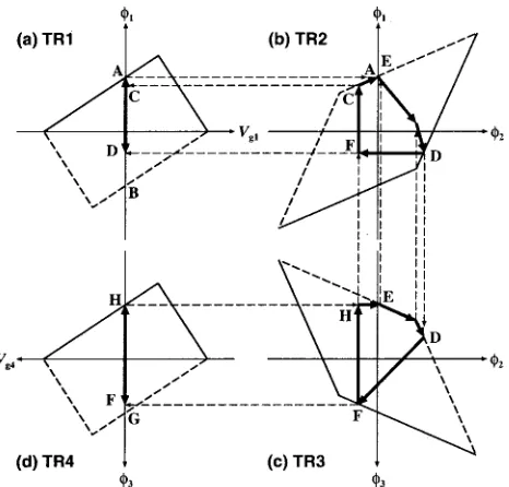
the space as clock pulses are applied. The pumping mecha-nism can be understood by considering the trajectory of the point. If the pump starts its operation from a neutral condi-tion共without any excess charges in the pump兲, it settles into a steady operation mode in a few clock cycles. Figure 4 schematically shows such a steady trajectory, projected onto four planes, each of which also shows the corresponding transistor’s stability rhomboid. The edge transistors are working in a somewhat different manner from other transis-tors, since one of their electrodes 共source or drain兲 is grounded, so that the -Vg planes are shown for them. The i⫺i⫹1 planes are shown for other transistors.
In Fig. 4共a兲 the state point moves between A and D. When Vp1 and hence 1 rises, the point moves toward A. However, before it reaches A, it reaches C in Fig. 4共b兲and
no other border is crossed anywhere else. Thus electrons enter the pump through the entrance transistor TR1 at A.
1共A兲⫽
e/2⫹CgVg1
C1⫹Cg⫹C0
共7兲
is the approximate upper bound of the voltage across the entrance transistor. When Vp1 starts falling and Vp2 starts
rising, the point moves from A to D in Fig. 4共b兲, whereas the point immediately reaches the unwanted border at E in Fig. 4共c兲and moves along the border. This means that electrons are tunneling from node3 to node2 through TR3. At D, the point is pinned and electrons flow from node1 to node2 through TR2. Next, the point moves from D to F and elec-trons move from node2 to node3 at F. This time no un-wanted tunneling occurs because G has not been reached in Fig. 4共d兲. Finally, the point goes to the last pinning point H and electrons are drained off node3 through TR4. Similarly to A, we see that
3共H兲⫽⫺
e/2⫺CgVg4
C2⫹Cg⫹C0 共
8兲
is the approximate lower bound for3.
The reverse-direction tunneling reduces the net current, and therefore should be prevented. With regard to the edge transistors, B and G should not be reached to prevent the reverse flow, whereas A and H should be for successful pumping. This tells us that Vg1 should be negative and Vg4
should be positive. Better still,
⫺ e
2Cg
⬍Vg1⬍⫺ e Cg
冉
1
2⫺
C2
C⌺
冊
共9兲and
e
Cg
冉
1
2⫺
C1
C⌺
冊
⬍Vg4⬍ e2Cg
共10兲
should be satisfied for smaller 兩1(A)/1(B)兩 and 兩4(H)/4(G)兩. The overlap of the clock pulses helps to keep the state point from reaching B and G by moving the point to the next transistors’ forward-direction borders. More intuitively, the falling pulse pushes electrons out of the present node, and the rising pulse pulls in the electrons to the next node. As for other transistors, the trajectory should not touch a border in the i–i⫹1 plane wheni increases, as
in Figs. 4共b兲 and 4共c兲. This will prevent tunneling in the unwanted direction through the corresponding transistor. But the trajectory should reach a border while i⫹1 increases. This leads to tunneling in the favorable direction. Whether these conditions are fulfilled depends on the choice of Vg1
[image:4.612.60.293.50.273.2]and Vg4 as well as on the position of stability rhomboids in
[image:4.612.320.519.509.588.2]the i⫺i⫹1 planes 关Fig. 2共b兲兴. We will simply leave the rhomboids at the center by setting Vg2 and Vg3 to zero, and change only Vg1 and Vg4. It should be noted that no clock
pulse pushes electrons from the ground into node1 while Vp1
rises nor does it pull electrons out of node3 to the ground while Vp3falls. The edge transistors therefore require special
consideration.
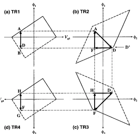
Figure 5 shows the steady trajectories for a set of well-chosen Vg1and Vg4. While the state point is moving from D
to A in Fig. 5共a兲, the point is always within the stability region for TR2 as shown in Fig. 5共b兲. As a consequence, electrons flow into node1 only through TR1 at A. Unlike in Fig. 4共b兲, the slope of the next segment of the trajectory,
AD, in Fig. 5共b兲 is⫺45° because no transistor is conduct-ing. Subsequently electrons flow through TR2 at D, next through TR3 at F, and finally through TR4 at H. Thus elec-trons are almost perfectly rectified in this case, and therefore it is an optimal operation condition. In this condition, the trajectories ini⫺i⫹1planes are isosceles right-angled tri-angles, so we will call it the ‘‘triangular condition.’’ In this case, only one transistor is conducting at a time, which means that packets of Nc electrons are indeed conveyed in
the pump.
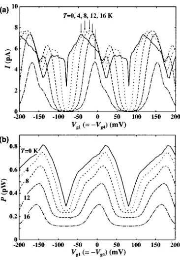
The net current and the power are plotted as a function of Vg1 in Figs. 6共a兲 and 6共b兲, respectively. The triangular condition occurs around the current maxima, where the power is not maximal. Although the power is not minimal in that condition, the net current flows only in the triangular condition when the clock amplitude Vp is small. One should
therefore use the triangular condition and smaller Vp to
re-duce the power. Otherwise, the pump will consume extra energy in vain.
The triangular condition also facilitates the estimation of
Nc and the power from the circuit parameters because
tun-neling events are localized to a particular transistor at each moment. By virtue of the perfect rectification, Ncequals the
number of electrons which enter the pump through TR1. Therefore
Nc⬇兵Vp⫺关1共A兲⫺1共D兲兴其/␦, 共11兲
where 1(A) is given by Eq. 共7兲 and ␦⬇e/CG. Pinning points like D in the i⫺i⫹1 planes are determined self-consistently. It is not straightforward to find the steady tra-jectories from a given set of side-gate biases. However, 1(D) may be approximated to1(D
⬘
).1共D
⬘
兲⫽⫺共C1⫹Cg⫹C0⫺C2兲e/2 共C1⫹Cg⫹C0兲共C2⫹Cg⫹C0兲⫺C1C2
. 共12兲
The simulation gives Nc⯝45.4. Using Eqs. 共7兲, 共11兲, and 共12兲, we obtain Nc⯝46.7, which is in good agreement with
the simulation.
Since only one transistor becomes conducting at a time and Nce is the charge that passes through it, the power
con-sumption due to tunneling is given by
P⫽f⫻Nce⫻
兺
iVdiff(i)
⫽f Nce兵1共A兲⫹关2共D兲⫺1共D兲兴
⫹关3共F兲⫺2共F兲兴⫺3共H兲兴其, 共13兲
where Vdiff(i) is the voltage drop across the ith transistor when it is conducting关cf. Eq.共1兲兴. By making use of Eq.共12兲,
2共D兲⫺1共D兲⬇
2共Cg⫹C0兲e
[image:5.612.345.533.47.309.2]共C1⫹Cg⫹C0兲共C2⫹Cg⫹C0兲⫺C1C2 共14兲
FIG. 5. Steady trajectories for well-chosen Vg1 and Vg4 at T⫽0 K. Vg2 ⫽Vg3⫽0 V. The state point draws triangles in thei⫺i⫹1planes.
FIG. 6.共a兲Net current I and共b兲power P as a function of Vg1for different
values of clock amplitude Vp. The triangular condition occurs at around
[image:5.612.62.293.51.275.2]and the same for 3(F)⫺2(F). Thus we can estimate the power to be P⯝0.6 pW. The simulation result is also P ⯝0.6 pW. We note that Eq. 共14兲 is a slight overestimate, whereas the simulation result includes the energy dissipation due to charging and discharging of capacitances.
The charge transfer mechanism in pumps with more transistors can be understood in the same way as the four-transistor pump. Steady trajectories in the i⫺i⫹1 planes become triangles at almost the same edge-transistor side-gate biases as the four-transistor case, and the approximation method presented above is also applicable mutatis mutandis. Although we have only tried adjusting side-gate biases of the edge transistors, one could further improve the pump operation by changing the capacitances of the edge transis-tors. For instance, as regards TR4, asymmetry of the rhom-boid about the V1 axis increases by making C1⬍C2. This leads to lesser 兩4(H)/4(G)兩, as can be seen from Fig. 3共a兲. Fine tuning of circuit parameters therefore is also an option worth exploring if sufficiently accurate fabrication technology is available.
V. TEMPERATURE AND FREQUENCY LIMITS
The main effect of nonzero temperature on the pump operation is to cause unwanted leakage current. At higher temperatures, the trajectories of a state point are no longer as simple as those in Figs. 4 or 5, and it is difficult to make good use of them. Qualitatively, stability rhomboids effec-tively shrink with temperature, so that the side-gate biases of the edge transistors that give a maximal current tend to shift toward zero, i.e., the middle of stability rhomboids. The magnitude of the effective shrinkage increases rapidly with
T, as ⌬F that gives the same leakage rate grows very
quickly; see Eq. 共4兲. The current is plotted in Fig. 7共a兲as a function of Vg1(⫽⫺Vg4) for different temperatures. The
current maxima approach Vg1⫽⫺Vg4⫽0 V as the
tempera-ture rises. At higher temperatempera-tures, some energy is supplied from the environment, so that the power consumption de-creases as expected, which is shown in Fig. 7共b兲.
Figure 8 shows the current in a three-transistor pump circuit as a function of the normalized phase delay f␦t 关see Fig. 1共c兲兴for two sets of side-gate biases for the edge tran-sistors, namely Vg1 and Vg3. In their experiment,
Tsuka-goshi et al. found f␦t⫽0.25 to be optimal.7 They also ob-served both positive and negative currents as they changed the phase delay. Figure 8共a兲, which is in the triangular con-dition at T⫽0 K, indicates the strong rectification in that condition, positive current is seen even with nonoptimal phase delay. However, as the temperature becomes higher, the net current vanishes rather quickly. With zero side-gate biases, current continues to flow up to much higher tempera-tures as shown in Fig. 8共b兲. The higher temperature results are in good agreement with the experimental results of Tsukagoshi et al.7 We suppose the experiment was carried out in this regime, where the temperature was not very low and the side-gate biases were near the middle of stability rhomboids.
The two characteristic temperature scales involved in the pump are e2/2C⌺kB⯝170 K and e2/2CGkB⯝9 K. The
high-est operation temperature is determined not by the small is-land capacitance C⌺ of the MTJ transistors but by the com-paratively large clocking-gate capacitance CG. This is
[image:6.612.349.535.48.320.2]because the state point spends much of the time around the
FIG. 7.共a兲Net current and共b兲power vs Vg1(⫽⫺Vg4) for various
tempera-tures. Vp⫽100 mV and f⫽1 MHz. FIG. 8. Net current vs normalized phase delay f␦t for different
[image:6.612.83.266.49.313.2]pinning points where the energy barrier for unwanted tunnel-ing is of the order of e␦.10Figure 9 plots the current and the power versus temperature for pumps with different num-bers of transistors. Figures 9共a兲and 9共c兲are in the triangular condition at T⫽0 K and Figs. 9共b兲 and 共d兲 are with zero side-gate biases. Again, zero side-gate biases tend to give more current at higher temperatures. The results confirm that the highest operation temperature is determined by CG.
Given the relative insensitivity to the temperature and to the transistor number seen in Fig. 9共b兲, the zero side-gate bias operation is a reasonable choice.
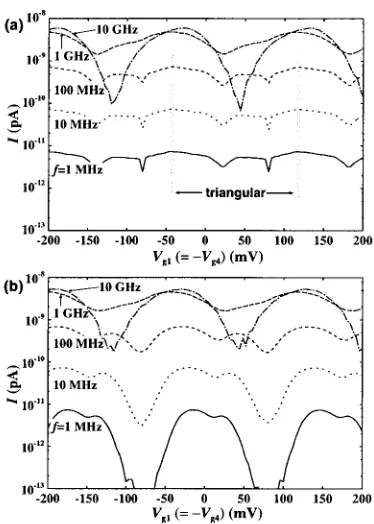
Too high a clock frequency f leads to missed tunneling events. After a state point has crossed a stability border, there is a finite time delay before tunneling takes place. At mod-erate frequencies, the delay is less than the time it takesito
change by␦, which we write as t␦⫽(␦/Vp)⫻(1/4f ). If
the delay is comparable to or longer than t␦, a pump cannot fully follow the clock signals and the pumping operation deviates from ideal.10 The upper frequency limit fmax for vanishing temperatures can be estimated as follows. The time delay approximates to the inverse of tunneling rate
⌫⫺1. It is convenient for the present purpose to express⌬F in the form ⌬F⫽⫺e(Vi⫹Vf)/2, where Vi and Vf are the voltages across the tunnel junction before and after tunnel-ing, respectively. In our case, Vi, f⬇⫾e/2C⌺, and at a suf-ficiently low frequency Vi⫹Vf→0. In the higher frequency
range we are interested in, Vi⫹Vf⬇␦, and hence ⌬F ⬇⫺e2/2CG. Using Eq. 共4兲 and I(V)⫽V/RT under kBT/⌬FⰆ⫺1,
1
t␦⫽
4Vpfmax
␦ ⬇⌫⫽2eR␦T. 共15兲
We therefore obtain
fmax⬇
e
8VpRTCG2 共16兲
as a rough estimate of the frequency above which the pump operation is expected to degrade. The numerical value for our simulation is fmax⬇1⫻108Hz, roughly above which the
current does not increase linearly with f , as confirmed in Fig. 10共a兲. We add that the threshold frequency depends on side-gate biases.
At nonzero temperatures, the delay becomes shorter and thermally activated tunneling 共with ⌬F⬎0兲 also occurs. Thermal errors affect pumping more at low frequencies,10 and it is seen as deeper current troughs in Fig. 10共b兲at low f . The upper frequency limit does not differ significantly from that for the zero-temperature case.
VI. DISCUSSION
We have investigated the operation of multiclocked pumps using a simplified model, assuming rather idealized situations, such as the uniformity of the pumps. We have derived approximate formulas which enable one to evaluate the number of electrons transferred per clock cycle and the power dissipation from a given set of circuit parameters. Be-cause of the restrictions imposed, our approximation method might be more useful as a means of estimating the best pos-sible performance achievable by such pump circuits, rather than as a means of understanding the details of nonideal, experimental results.
The estimated operation temperature and frequency are not particularly high even with the relatively optimistic nu-merical values used in the simulations. The power consump-tion, on the other hand, is very low. This is because of the small number of electrons involved and the low operation voltage. Operation with a much higher clock frequency, e.g.,
fmax, is perfectly acceptable in this capacitance range, as far as power is concerned. If the entire circuit is scaled down with keeping the ratio C⌺/CG constant, higher values of
[image:7.612.345.532.48.310.2]temperature and frequency would be achieved in theory. However, the scaling also means operation with accordingly
FIG. 9. Current and power vs temperature for different numbers of transis-tors in a pump.共a兲and共c兲are in the triangular condition at T⫽0 K. For共b兲 and共d兲all side-gate biases are 0 V.
[image:7.612.56.296.52.230.2]advantage over conventional circuits in this regard. Of course, whether such miniaturization is possible is another issue. Also, we did not consider the change in RTby scaling
down.
With respect to the BDD logic application, it is hoped that only one electron packet is sufficient as the medium of bit information, thereby realizing a high throughput. In fact, in the logic operation experiment reported by Tsukagoshi
et al., a large number of packets were used because of the
very slow logic operation speed.13 We found by simulation that it takes several cycles for a pump to settle into a steady trajectory. Furthermore, the longer the pump is, the longer it takes to settle. This might imply a possible difficulty with the single-packet operation scheme. Further study with an appro-priate model of the switching device is needed to explore the prospects for an efficient logic application.
ACKNOWLEDGMENTS
The authors thank Professor H. Ahmed and Dr. K. Tsukagoshi for support and discussions. S. A. thanks Profes-sor K. Hoh for support. This work was carried out under the management of FED as a part of the MITI R&D of Industrial Science and Technology Frontier Program共Quantum Func-tional Device Project兲supported by NEDO.
3972共1997兲. 7
K. Tsukagoshi and K. Nakazato, Appl. Phys. Lett. 71, 3138共1997兲. 8
K. Nakazato, R. J. Blaikie, and H. Ahmed, J. Appl. Phys. 75, 5123共1994兲. 9K. Nakazato and H. Ahmed, Jpn. J. Appl. Phys., Part 1 34, 700共1995兲. 10M. B. A. Jalil, H. Ahmed, and M. Wagner, J. Appl. Phys. 84, 4617共1998兲. 11J. Weis, R. J. Haug, K. v. Klitzing, and K. Ploog, Semicond. Sci. Technol.
10, 877共1995兲.
12K. Tsukagoshi and K. Nakazato, Appl. Phys. Lett. 72, 1084共1998兲. 13
K. Tsukagoshi, B. W. Alphenaar, and K. Nakazato, Appl. Phys. Lett. 73, 2515共1998兲.
14J. M. Rabaey, Digital Integrated Circuits: A Design Perspective共Prentice Hall, Upper Saddle River, New Jersey, 1996兲.
15D. V. Averin and K. K. Likharev, in Single Charge Tunneling, edited by H. Grabert and M. H. Devoret共Plenum, New York, 1992兲, Chap. 9, p. 311.
16The circuit is assumed to be in thermal equilibrium with the environment. 17K. K. Likharev, IBM J. Res. Dev. 32, 144共1988兲.
18S. Amakawa, H. Majima, H. Fukui, M. Fujishima, and K. Hoh, IEICE Trans. Electron. E81-C, 21共1998兲.
19M. Kirihara, K. Nakazato, and M. Wagner, Jpn. J. Appl. Phys., Part 1 38, 2028共1999兲.
20
K. K. Likharev, IEEE Trans. Magn. 23, 1142共1987兲. 21H. Tamura and S. Hasuo, J. Appl. Phys. 62, 3036共1987兲. 22These inequalities only define the stable region for the state m