OPTOELECTRONIC APPLICATIONS
Xin Li
A Thesis Submitted for the Degree of PhD
at the
University of St Andrews
2019
Full metadata for this item is available in
St Andrews Research Repository
at:
http://research-repository.st-andrews.ac.uk/
Please use this identifier to cite or link to this item:
http://hdl.handle.net/10023/18938
Optoelectronic Applications
Xin Li
This thesis is submitted in partial fulfilment for the degree of
D
octor of
P
hilosophy
at the
U
niversity of
S
t
A
ndrews
School of Physics and Astronomy
University of St Andrews
KY16 9SS
http://synthopt.wp.st-andrews.ac.uk/
My PhD is focused on the design, fabrication and optoelectronic applications of epsilon-near-zero (ENZ) metamaterials (MMs), which have vanishing real part of the permittivity and support fascinating optical effects, including light squeezing, sub-wavelength imaging, enhanced directive emission and enhanced non-resonant optical nonlinearity. Different approaches have been developed to realise ENZ media, such as tuning the modal dispersion in narrow plasmonic channels, exploiting the natural dispersion of transparent conductive oxides and creating composite structures with metals and dielectrics. As a platform with exotic physical properties, ENZ media also exhibit enormous potentials in combination with tunability and various nanofeatures in the photonic and plasmonic regimes.
This thesis demonstrates two approaches to achieve the ENZ condition. One method is to stack metal (Ag) and dielectric (SiO2) layers periodically at sub-wavelength scales. The resulting material
behaves as an effective medium with an average permittivity close to zero, and we show that this ENZ medium can enhance the emission of quantum dots. This approach generally requires nanofabrication techniques developed for flat and rigid substrates, for example, the electron beam evaporation, which are not always applicable to micro- and macroscopic devices with arbitrary shapes. To surpass these limitations, we design and experimentally demonstrate an optical free-standing and low-loss ENZ membrane in the visible range, by layering polymer (SU-8) and Ag nano-layers. Additionally, we propose a method to introduce both flexibility and electrical tunability into ENZ media by replacing the metal layer with a 2D material, graphene, in the multilayer model. The other way to obtain an ENZ response is using natural materials which operate in prox-imity of their plasma frequency, typically here the indium tin oxide (ITO) at the near-infrared range. The ITO thin films are deposited using radio frequency magnetron sputtering, and their permittivities are manipulated via controlling fabrication parameters. We succeed in sweeping the zero-permittivity frequency of ITO media by controlling the gas recipe and deposition temperature during the sputtering process. To obtain specific optical responses, the ENZ ITO thin films are designed to be combined with different photonic features, including nanoantenna on microsphere and nanohelix, associated with a direct fabrication approach based on electron beam induced deposition (EBID).
I, Xin Li, do hereby certify that this thesis, submitted for the degree of PhD, which is approximately
50,000 words in length, has been written by me, and that it is the record of work carried out by
me, or principally by myself in collaboration with others as acknowledged, and that it has not been
submitted in any previous application for any degree.
I was admitted as a research student at the University of St Andrews in September 2015.
I received funding from an organisation or institution and have acknowledged the funder(s) in the
full text of my thesis.
Date Signature of candidate
Supervisor’s declaration:
I hereby certify that the candidate has fulfilled the conditions of the Resolution and Regulations
appropriate for the degree of PhD in the University of St Andrews and that the candidate is qualified
to submit this thesis in application for that degree.
In submitting this thesis to the University of St Andrews we understand that we are giving
permis-sion for it to be made available for use in accordance with the regulations of the University Library
for the time being in force, subject to any copyright vested in the work not being affected thereby.
We also understand, unless exempt by an award of an embargo as requested below, that the title
and the abstract will be published, and that a copy of the work may be made and supplied to any
bona fide library or research worker, that this thesis will be electronically accessible for personal or
research use and that the library has the right to migrate this thesis into new electronic forms as
required to ensure continued access to the thesis.
I, Xin Li, confirm that my thesis does not contain any third-party material that requires
copy-right clearance.
The following is an agreed request by candidate and supervisor regarding the publication of
this thesis:
PRINTED COPY
No embargo on print copy
ELECTRONIC COPY
No embargo on electronic copy
Date Signature of candidate
Candidate’s declarations:
I, Xin Li, understand that by declaring that I have original research data or digital outputs, I should
make every effort in meeting the University’s and research funders’ requirements on the deposit and
sharing of research data or research digital outputs.
Date Signature of candidate
Permission for publication of underpinning research data or digital outputs
We understand that for any original research data or digital outputs which are deposited, we are
giving permission for them to be made available for use in accordance with the requirements of the
University and research funders, for the time being in force.
We also understand that the title and the description will be published, and that the underpinning
research data or digital outputs will be electronically accessible for use in accordance with the license
specified at the point of deposit, unless exempt by award of an embargo as requested below.
The following is an agreed request by candidate and supervisor regarding the publication of
underpinning research data or digital outputs:
No embargo on underpinning research data or digital outputs.
Date Signature of candidate
The completion of my PhD work is attributed to the help and encouragement of many people, and
thus here I would like to express my gratitude to all of them sincerely.
My biggest thanks go first and foremost to Dr Andrea Di Falco, my supervisor, for giving me the
excellent opportunity to study at St Andrews. I do appreciate his consistent encouragement, expert
guidance and meaningful inspirations, which help me understand my research better and produce
this thesis. Without his support and constant feedback, my PhD would have never completed.
Next, I would like to thank Prof. Robert Thomson and Dr Liam O’Faolain for agreeing to be my
examiners.
I greatly appreciate the support received from the members of the Synthetic Optics Group:
Usenobong Akpan, Danielle Fraser, Sophie Varney, Yunli Qiu and Xiangkun Kong. Particularly,
Adam Fleming, James Burch, Alasdair Fikouras and I started the PhD at the same time, and hopefully,
we would finish our work at the same period. Special thanks go to Blair Kirkpatrick, Monika Pietrzyk
and Aline Heyerick for training me various pieces of equipment in both cleanrooms and laboratories.
I would also like to thank the members of the Nanophotonics Group in St Andrews, particularly
Changyu Hu and Alexandros Liles for helping me understand the procedure of electron-beam
lithography, and Dr Sebastian Schulz, who has shown me how to run FDTD simulations.
In the School of Physics and Astronomy more generally, I would like to extend my gratitude to
Callum Smith, Chris Watson and Graeme Beaton, who have kept the cleanroom facilities working
perfectly and assisted the modification of laboratory apparatus when necessary. Besides, I should
particularly thank Scott Johnston, the Stores Manager of our school, for his great effort on ordering
equipment and consumables. My faithful appreciation also goes to Lesley Aitken, Linda Cousins
Aaron Naden and Richard Bailey, who have helped me about the fabrication and characterisation
using focused ion beam system and atomic force microscope. I should also thank Dr Emanuele
Pelucchi from Tyndall National Institute, University College Cork, Cork, Ireland, for providing me
with the pyramid samples which are essential for the research of photonic trimming of quantum
emitters.
Last but not least, I would like to express my sincere thanks to my parents, who supported me
in all my pursuits and motivated me to confront any obstacles on my way to success. Notably, the
deepest thanks of all must go to Jie, my girlfriend, for her accompanying and supporting without a
word of complaint all the time.
Collaboration Statement
I would like to acknowledge Dr Zhang-Kai Zhou and Dr Ying Yu from the School of Physics and
Engineering, Sun Yat-sen University, Guangzhou, China, for their collaboration with the work
of photonic trimming of quantum emitters via direct fabrication of metallic nanofeatures. Their
teams provided me with the samples of nanowires and micropillars that hosted quantum dots and
performed emission analysis experiments. Their help was precious when I visited Guangzhou.
Acknowledgement of funding
This work was supported by the China Scholarship Council and the University of St Andrews (School
of Physics and Astronomy).
Research Data access statement
Research data underpinning this thesis are available at
Publications
• Li, X., Su, R.L., Zhou, Z.K., Yu, Y. and Di Falco, A. "Photonic trimming of quantum emitters
via direct fabrication of metallic nanofeatures." APL Photonics, 3(7), 071301(2018).
• Rizza, C.,Li, X., Di Falco, A., Palange, E., Marini, A. and Ciattoni, A. "Enhanced asymmetric
transmission in hyperbolic epsilon-near-zero slabs." Journal of Optics, 20(8), 085001(2018).
• Li, X., Rizza, C., Schulz, S. A., Ciattoni, A. and Di Falco, A. "Conformable optical coatings with
epsilon near zero response." APL Photonics, 4(5), 056107(2019).
Conferences
• Pietrzyk, M.,Li, X., Rishad, K., Faccio, D., and Di Falco, A. "Epsilon Near Zero Metamaterials
for Nonlinear Optics Applications."ADVANCED MATERIALS CONFERENCE, 2016. Poster,
presented by Pietrzyk, M.
• Li, X., Pietrzyk, M., Rizza, C., Scalora, M., Ciattoni, A., and Di Falco, A. "One-Dimensional
Chirality: Strong Optical Activity in Epsilon-Near-Zero Metamaterials."The 12th International
Symposium on Photonic and Electromagnetic Crystal Structures (PECS-XII), 2016. Poster, presented
byLi, X..
• Li, X., Pietrzyk, M., Faccio, D., Rizza, C., Ciattoni, A. and Di Falco, A. "Linear and nonlinear
optical behavior of epsilon near zero metamaterials: opportunities and challenges."Proc. SPIE
10111, Quantum Sensing and Nano Electronics and Photonics XIV, Vol. 10111, p. 101111O, 2017.
Symposium, 2017. Poster, presented byLi, X..
• Li, X., Zhou, Z.K., Yu, Y., Gather, M. and Di Falco, A. "Nanophotonic enhanced quantum
emitters." Proc. SPIE 10359, Quantum Nanophotonics, Vol. 10359, p. 103590A, 2017. Talk,
presented by Di Falco, A.
• Li, X., Rizza, C., Ciattoni, A., Faccio, D., and Di Falco, A. "Photonic Applications of Epsilon
near Zero Metamaterials."Progress in Electromagnetics Research Symposium (PIERS) 2018, 2018.
Talk, presented by Di Falco, A.
• Rizza, C.,Li, X., Di Falco, A., Palange, E., Marini, A. and Ciattoni, A. "Optical chiral effects
in ENZ ultrathin slabs."META 2018 , the 9th International Conference on Metamaterials, Photonic
Crystals and Plasmonics, 2018. Talk, presented by Rizza, C.
• Li, X., Zhou, Z.K., Yu, Y., and Di Falco, A. "Nanoplasmonic enhancement of semiconductor
quantum emitters."The 18th IEEE International Conference on Nanotechnology, 2018. Talk,
presen-ted byLi, X..
• Rizza, C.,Li, X., Di Falco, A., Palange, E., Marini, A. and Ciattoni, A. "Diode-like asymmetric
transmission in hyperbolic epsilon-near-zero media." Nanophotonics and Micro/Nano Optics
Acknowledgements v
Publications and Conferences viii
Contents x
1 Introduction 1
1.1 A historical overview of MMs and ENZ MMs . . . 1
1.2 Light propagation in ENZ media . . . 5
1.3 Applications of ENZ medium in the emission enhancement . . . 7
1.4 Enhanced optical nonlinearity at ENZ range . . . 8
1.5 Structure of the thesis . . . 8
2 Background and theory 10 2.1 Realisation of ENZ MMs . . . 10
2.2 Optical wave modification inside ENZ MMs . . . 15
2.3 Asymmetric transmission enhanced by the AENZ slab . . . 18
2.4 Emission enhancement on the ENZ substrate . . . 23
2.5 Summary . . . 25
3 Fabrication, characterisation of multilayer ENZ structures and related emission enhance-ment 26 3.1 Overview . . . 26
3.3 Characterisation . . . 31
3.4 Emission enhancement on ENZ substrates . . . 43
3.5 Conclusion . . . 54
4 Flexible ENZ MMs 56 4.1 Motivation . . . 56
4.2 Fabrication . . . 57
4.3 Characterisation . . . 61
4.4 Results and discussion . . . 65
4.5 Conclusion . . . 68
5 Graphene-based ENZ MMs 69 5.1 Motivation . . . 69
5.2 Numerical modelling of graphene/PMMA multilayer structure . . . 70
5.3 Fabrication and transfer of graphene . . . 73
5.4 Characterisation of graphene . . . 80
5.5 Realisation of graphene/PMMA multilayer structure . . . 89
5.6 Electrical tuning graphene/dielectric structure at infrared range . . . 92
5.7 Conclusion . . . 98
6 ITO and applications associated with EBID 99 6.1 Fabrication of ITO . . . 99
6.2 Charaterisation of ITO . . . 101
6.3 Applications of ITO associated with EBID . . . 106
6.4 Photonic trimming of QDs emission using EBID approach . . . 113
6.5 Conclusion . . . 124
7 Conclusion 126 7.1 Thesis summary . . . 126
7.2 Outlook . . . 127
Bibliography 130
List of Figures 151
Introduction
This chapter briefly introduces the main content of this thesis, addressing first the historical
develop-ment of metamaterials (MMs) and epsilon-near-zero (ENZ) MMs, and types of ENZ structures, then
the typical light propagation with no spatial dispersion through ENZ media. This part also shows
specific applications of ENZ structures, such as non-diffraction imaging, enhanced directive emission
and nonlocal enhancement in nonlinear optics. The final section outlines the structure of this thesis.
1.1
A historical overview of MMs and ENZ MMs
Photonic MMs are artificial materials typically consisting of sub-wavelength repeating patterns
and exhibiting peculiar properties[1, 2]. The prefix "meta" means "beyond" in Greek[3], and it
indicates that MMs exhibit physical properties which not present in natural materials. These unusual
properties result from the homogenisation of component structures, which is also beyond the simple
sum of every component. As the size of the component atoms is much smaller than the wavelength of
probing electromagnetic wave, MMs exhibit macroscopic properties that are not shown in constituent
materials. Particularly, in the visible and near-infrared (NIR) regime, the scale of unit structures in
MMs goes down to tens of nanometres or less. Because of the shared scales, the field of MMs has
involved in parallel with that of plasmonics[4].
The study of plasmonics and MMs first began thousands of years ago. For example, the Lycurgus
Cup[5, 6] constructed with ruby glass in the 4th century shows different colours when light shines
from inside and outside the cup. This phenomenon is caused by the nanoscale (5 - 60 nm) gold
(Au) and silver (Ag) particles embedded in the ruby glass. The nanoparticles scatter light with high
sensitivity to their sizes and exhibit dichroic characteristic due to the plasmon resonance[7]. Hence,
mechanics of the Lycurgus Cup were not fully understood a thousand years ago, the manufacturing
technique has been passed on and has motivated research into plasmonics[8] and MMs[6].
Classical electrodynamics shows that the electromagnetic properties of materials depend on their
permittivity () and permeability (μ). The refractive index (n) of a material is defined as
n=√μ (1.1)
Asandμare determined by microscopic properties and distributions of atoms inside materials, the development of MMs permits to extend the optical properties beyond those enabled by these
atomic configurations.
The theoretical research into plasmonic materials started from the study of negative refraction by
Mandelshtam in the 1940s[9]. In 1968, an important step was made by Veselago who presented a
theoretical work on the negative-index materials (NIMs) (also known as left-handed materials)[10]
whoseandμare all negative. He predicted that negative refraction which is never seen in nature would exist inside this kind of material. However, the real investigation and design of NIMs did
not begin in earliest until about 30 years later. In 1996, Pendry et al. proposed a structure that
consisted of periodic aluminium (Al) microwires that could exhibit a negativeat GHz range[11]. Three years later, Pendry et al. also proposed that a periodic split rings array made of nonmagnetic
material could exhibit a negativeμ[12]. Eventually, in 2000 and 2001, Smith et al. demonstrated the experimental realisation of the first one-dimensional (1D)[13] and two-dimensional (2D)[14] NIMs
using a structure combining split ring resonators with wires. These studies of NIMs provided the
possibility to modify theandμof materials artificially and motivated the development of other MMs.
As mentioned above, the structural units of MMs usually have a size which is far smaller
than the working wavelength. This is because the MMs typically have inhomogeneous structure
and complex boundary conditions, and many physical properties of them (e.g. and μ) cannot be calculated precisely and easily. A common way to approximate the effective electromagnetic
properties of these media in theory is using the effective medium theory (EMT)[15, 16]. The EMT
can describe the macroscopic properties of composite materials (e.g. MMs) by averaging the related
physical parameters of the composite materials, with the request of limiting the size of the structural
units within the sub-wavelength scale. Therefore, here we use a common approach to design and
characterise MMs using effective permittivity (e f f) and permeability (μe f f) based on EMT and this
Figure 1.1: Diagram of a MM made of periodic sub-wavelength unit structures and the corresponding effective medium. To satisfy the demand of EMT, the period (Λ) of the structure is far less than the wavelength (λ) of the electromagnetic wave.
Due to the ability of modifying effectiveandμ, MMs now show dramatic potential in the field of high-directivity radiating[17], electromagnetic cloaking[2, 18], perfect absorbing[19] and quantum
applications[20].
As special MMs, zero-index materials (ZIMs) show vanishing refractive index at specific
frequen-cies and has attracted much attention in many research fields, such as emission controlling[21] and
Figure 1.2: Parameter space ofμvs, and the location of ENZ MMs.
Theof natural substances can be both positive (e.g., dielectric material) or negative (e.g., most metal materials). However, theμvalue is usually equal to 1, due to the weak magnetic repose of most natural materials at a high-frequency range. The assumptionμ=1 will be used in this thesis as there are no ferromagnetic materials or magnetic structure used in this work, and this ENZ MM is
indicated in Figure 1.2. Therefore, Equation 1.1 can be simplified as
n=√ (1.2)
Additionally, complicated structures and processes are always needed to realise double-zero ZIMs,
i.e. reaching zeroμandat same time[22]. However, it is relatively easy to obtain zero-permittivity structure using non-magnetic materials[23]. Therefore, the zero-index condition can be obtained at
ENZ media, according to Equation 1.2.
Inside ENZ MMs, due toapproaching zero, the refractive index, effective displacement field and the wave vector are all close to zero, thus the wavelength diverges and no diffraction occurs. The
ENZ MMs can be classified in two types: anisotropic epsilon-near-zero (AENZ) MMs and isotropic
epsilon-near-zero (IENZ) MMs. AENZ condition is realised based on EMT, usually by averaging the
positive and negative permittivity contributed by different sub-wavelength components, typically
dielectrics and metals[24, 25]. Under this condition, one component of the effective permittivity
the transmission in specific directions. The other type ENZ condition, i.e. IENZ, is achieved by
transparent conductive oxides (TCOs)[26], such as Al-doped zinc oxide (AZO), indium tin oxide
(ITO) and gallium zinc oxide (GZO). Their permittivity can be tuned by modifying their plasma
frequency, and typically approaches zero at NIR range. In addition, TCOs have small optical losses
and electric tunability, and thus displays potentials to be used in wider-range optoelectronic devices.
These peculiar properties have attracted significant attention in the last two decades. In 2002,
Enoch et al. demonstrated a method for tuning the emission of an antenna embedded in a multilayer
metal-grid material[21]. By changing the parameters of unit structures, the effectivewas modified, and the directive emission was realised in the ENZ condition. In 2006, Silveirinha et al. presented a
theoretical work on the tunneling effect in ENZ MMs[27]. The electromagnetic waves were "squeezed"
through arbitrary shaped ENZ channels with almost no phase variation. This effect was verified
experimentally by Liu et al.[28] and Edwards et al.[29] in 2008. Based on this, the perfect bending
waveguides were designed by Luo and Lai et al.[30, 31] and realised experimentally by Ma et al.[32].
Further research done by Luo et al. showed that AENZ MMs had the capability of controlling
electromagnetic flux conveniently and efficiently[33].
In recent years, ENZ MMs have shown important and interesting physical properties, and
enormous potential in applications such as sub-wavelength imaging[34], optical sensing[35] and
asymmetric transmission[36]. However, the study of ENZ MMs is still a basic research, and further
theoretical research and experimental design need to be investigated.
1.2
Light propagation in ENZ media
Media with vanishing refractive index show unique dielectric responses and promise the possibility
of light manipulation. A simulation work has predicted that a time varying source in a matched
zero-index material (ZIM) exhibits a constant spatial distribution within the medium[37], and the 1D
distribution of the electric field is sketched in Figure 1.3 (a).
The region marked by two vertical dashed black lines shows the position of free space or a ZIM.
The other parts outside the two boundaries are filled with lossy media. A line source locates at the
middle of the medium region and emits light waves towards both the left and right boundaries. The
dashed blue line in Figure 1.3 (a) shows a steady-state oscillation of the light wave inside the free
space and a fast decay in the lossy media. The solid red line presents the distribution of electric
field of the light inside the ZIM at a moment when the light just propagate to the inflection points,
varying in time, as source is varying with time. After the light travel through the whole medium, the
electrical field will exhibit a fast decay similar to the blue dashed line. This effect is due to the zero
phase variation and diverging wavelength inside the ZIM, and there is no phase difference between
two points in the ZIM.
Figure 1.3: Diagrams of light propagating through ZIM (n≈0) and ENZ medium. (a) The light come from a line source (green vertical line) exhibit constant electric field in the ZIM (red solid line) while shows steady-state electric field in free space (blue dashed line)[37]. The two vertical dashed black lines are the boundaries of the ZIM or free space. The left and right regions beside the medium region are filled with lossy media. (b) An ENZ medium manipulate the shape of a wavefront from arbitrary to the same as exit surface[38].
As discussed above, the zero-index condition can be approached in ENZ MMs[39]. Another
simulation work has predicted that the phase variation also approaches zero or effectively very small
inside a ENZ slab[38], and this effect opens the door towards the direct modification of wavefront.
As Figure 1.3 (b) illustrated, a electromagnetic wave with arbitrary shaped wavefront propagates
through an ENZ medium from entrance side, and the phase distribution at the exit side is conformal
with the shape of the exit surface. Therefore, by designing the exit surface of ENZ media, the
impinging wave can be manipulated and the phase distribution can be transformed into a desired
shape. The challenge of this design is the coupling of the input wave to the ENZ medium, which
needs more investigation.
Due to the small permittivity, ENZ MMs also have negligible spatial dispersion. Spatial dispersion
is defined here as the dependence between permittivity and wave vector or wavelength in a medium.
Therefore, the wavelength of electromagnetic waves will be stretched inside ENZ media[34]. These
Figure 1.4 sketches a curved metal-dielectric multilayer structure which is designed to exhibit zero
effective permittivity in the directions perpendicular to the stacking direction. The optical waves
from two point sources separated in sub-wavelength scale will propagate through the structure
nondiffractively. The output light spots are exactly copied from the sources, and with the help of
symmetric curvature, the magnification beyond diffraction limits can be achieved.
Figure 1.4: 2D diagram of a curved AENZ medium whose inner layer to which two light sources are attaching that separated in sub-wavelength scale[34]. After propagating through the ENZ medium, the two output light spots are separated with a distance large enough to break the diffraction limit.
Additionally, ENZ media can support electromagnetic chirality which usually only shown
in three-dimensional (3D)[40] or 2D[41] complex chiral structures. Chirality has drawn a great
deal of attention[42, 43] in the field of molecular biology and life science, associated with optics,
crystallography and particle physics. Generally, the chiral response, i.e. the asymmetric transmission,
can be achieved by breaking either the Lorentz reciprocity[44] or the spatial inversion symmetry[42].
With the help of considerable the magneto-electric coupling, the ENZ structure shows dramatical
enhancement of the optical chirality[36].
1.3
Applications of ENZ medium in the emission enhancement
Due to the near-zero effective permittivity, ENZ MMs have vanishingly small refractive indices. In this
situation, most media in nature, even the air, are optically "denser" than ENZ media. Therefore, total
reflection will occur when light propagates from a ENZ slab to other "denser" material. Considering
the interface between a ENZ slab and air, when a light source (e.g. dipole) is placed on top of
or immersed inside the ENZ medium, the radiation intensity in the air side can be enhanced
This effect has been used to enhance the emission of antennas. For example, the molecular
fluorescence can be boosted inside a ENZ waveguide and the enhancement is independent of the
location of the emission source[46]. In another model, the emission of plasmonic antennas can be
enhanced dramatically by a ENZ substrate[47].
Additionally, due to the lack of spatial dispersion, the emission of point source embedded inside
ENZ slabs can be modified into a plane wave with enhanced directivity and efficiency[48].
These characteristics make it possible to realise the superradiance, beam steering and the
manip-ulation of quantum emission.
1.4
Enhanced optical nonlinearity at ENZ range
Nonlinear response of optical materials draws a great deal of attention and generate fascinating
applications, such as optical harmonic generation[49], transient coherent effect[50] and self-focusing
of optical beams[51]. Additionally, these nonlinear effects can be supported at ENZ MMs.
The mechanisms of nonlinear optics can be classified as resonant or nonresonant, according
to the relationship between the frequency of light and the particular electronic resonances of the
material[52, 53]. Nonresonant nonlinearities are generally weak and require high light intensities
and/or very long light-matter interaction time and length[54]. On contrast, resonant nonlinearities
can be several orders of magnitude stronger, but this comes at the cost of introducing detrimental
and unavoidable losses[55, 56].
Under the ENZ condition, due to the linear permittivity approaching zero, the linear refractive
index is relatively small compared to the nonlinear susceptibility, hence the nonlinear response
can be obtained with low-power probing and low losses[57]. In the interface between vacuum and
ENZ medium, the nonresonant enhancement of the typical electric field can combine the ENZ effect
with nonlinearity[58], which leads to peculiar nonlinear effects, such as transmissivity directional
hysteresis[59] and enhancement of second and third harmonic generation[60, 61].
1.5
Structure of the thesis
This thesis starts with an introduction of the historical development and particular properties of
ENZ MMs. Different ENZ platforms have been introduced for typical applications, such as light
squeezing, sub-wavelength imaging, enhanced directive emission and enhanced nonresonant optical
Chapter 2 discusses the background theory of light-matter interaction in ENZ regime, which
related to the works in the following chapters. The first section is about the realisation of ENZ
structure, including mainly two models, i.e. the metal/dielectric multilayer structure according to
EMT and TCOs which operate near their plasma frequency based on Drude-Sommerfeld model.
Then, light modification, asymmetry transmission and enhanced directive emission based on ENZ
media will be presented, followed by a summary.
Chapter 3 demonstrates the fabrication and characterisation of Ag/silicon dioxide (SiO2)
mul-tilayer ENZ structure. The Ag and SiO2nanolayers are deposited using an electron beam (e-beam)
evaporation technique, which is addressed in detail. To optically characterise thin films, we present
a retrieval method based on Fresnel’s equations. Finally, the investigation of the ENZ platform for
enhancing the emission of quantum dots (QDs) is presented, before the summary.
Chapter 4 details the way to introduce flexibility into ENZ membranes using a sacrificial-layer
assisted method. First, the complete fabrication process of the multilayer metal/polymer structure
is demonstrated in detail. Next, we test optical properties of the material after large mechanical
deformations and also show the capability of this membrane to conform on targets with irregular
surfaces. The flexibility promises the feasibility of ENZ structures in superlens and other shape
sensitive applications. In the end, the conclusion is presented.
Chapter 5 outlines the design of graphene-based ENZ structure which provides the possibility
to introduce both flexibility and electrical tunability into multilayer graphene/dielectric structures.
The fabrication of graphene using chemical vapour deposition (CVD) method is first demonstrated,
followed by the characterisation of graphene using optical, electrical and physical means. Then we
show the fabrication of flexible graphene/dielectric membrane and the initial result of the electrical
tuning at NIR range.
Chapter 6 concerns about the fabrication of ITO thin films using radio frequency (RF) magnetron
sputtering approach. First, the deposition and characterisation of ITO films with tunable permittivity
via modifying the deposition parameters are presented. Then, we propose that the ENZ ITO material
can be combined with different nanofeatures, fabricated directly using electron beam induced
deposition (EBID) method, to realise typical optical responses. Additionally, the other applications
based on the EBID technique are also addressed.
Background and theory
This chapter gives a general review of the background and fundamental physics of ENZ MMs.
The first section outlines the approaches of realising ENZ structures, both in anisotropic and
homogeneous configurations. Next, the optical wave modification in ENZ regime is discussed,
particularly the phase variation minimisation and wavefront engineering. After that, the non-local
enhancement of asymmetry transmission in ENZ regime is addressed in detail. This section is my
original work with collaborators. The next section briefly discuss the emission enhancement related
to ENZ MMs. The final part summarises the optical properties and further applications of ENZ
membrane included in this thesis.
2.1
Realisation of ENZ MMs
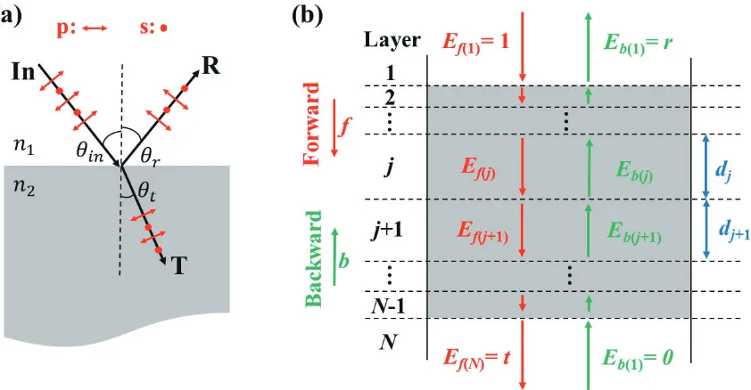
The ENZ condition can be approached using different methods, sketched in Figure 2.1. One way is
according to EMT via stacking materials with positive (e.g. dielectric) and negative (e.g. metal) alternatively in the sub-wavelength regime (Figure 2.1 (a))[25]. This method is able to create uniaxial
AENZ MMs. The perpendicular (to the stacking direction) components of the effectivecan be tuned into zero by simply modifying the thicknesses of unit layers, while the parallel component usually
retains the value bigger than 1. This approach can be also used in 2D model by patterning periodic
structures consisting of complementary split ring resonators[28] or nanorods[24]. As shown in Figure
2.1 (b), the metal nanorod array is embedded in dielectric medium (such as aluminium oxide (Al2O3))
or surrounded by air and this structure can be designed to exhibit a vanishing effective permittivity
Figure 2.1: Diagram of three types of ENZ structures. (a) a periodic structure consisted of two unit layers: metal with thicknesstmand permittivitym; dielectric with thicknesstdand permittivityd. ⊥andare the perpendicular and parallel components of the effective permittivity of the structure. (b) a 2D ENZ structure consisted with metal nanorods embedded in dielectric environment. (c) TCOs slab whose permittivity can reach zero at near-infrared ranges.
Another method of obtaining ENZ response is based on the materials operated closed to their
plasma frequency, such as TCOs (Figure 2.1 (c))[62]. Plasma frequency is an intrinsic property of
conducting materials, such as metals, semiconductors and TCOs, and determines the permittivity
of these materials according to Drude-Sommerfeld model[63]. When these media interact with
electromagnetic waves, free carriers (e.g. electrons) inside them oscillate with a frequency which
is related to the density, charge and effective mass of carriers. Additionally, the frequency of this
oscillation is independent of the wavelength of input waves. This frequency is so called plasma
frequency. Typically, if the operating frequency is lower than the plasma frequency, the medium
shows a negative permittivity; if the operating frequency is higher than the plasma frequency, the
medium shows a positive permittivity. This effect promises the ENZ response of TCOs when they
are operated near their plasma frequency. Specifically, here we use a special TCOs, i.e. ITO, and its
permittivity approaches zero at NIR ranges. This material will be discussed in detail later in this
chapter.
In this thesis, I focus on the two approaches shown in Figure 2.1 (a) and (c), i.e. the anisotropic
metal/dielectric multilayer structure and homogeneous (isotropic) ENZ medium (e.g. ITO).
2.1.1
Realisation of AENZ MMs
In the optical regime, most metals show negative dielectric response because the optical frequency
(ω) is much higher than their plasma angular frequency (ωp), and their dielectric permittivity (m)
m(ω) =b− ω2
p
ω2+iγω (2.1)
wherebrepresents the background permittivity,γis the collision frequency which is typically
essential and related to optical losses.
Inside these metal materials, whenm<0, the internal free carriers move in the opposite direction
to the external electric field. On the contrary, dielectric materials have positive permittivities (d>0).
To obtain the material with tunable permittivity, we can consider the simplest model, i.e. the 1D
periodic structure consisting of repeating metal-dielectric bilayers (Figure 2.1 (a)). Each metal layer
has a thickness of tm and permittivity ofm, and each dielectric layer has a thickness of td and
permittivity ofd. Using this structure, we can realise the capability to modify the effectiveand
also achieve the ENZ condition.
In sub-wavelength situation, the multilayer structure shows anisotropic effective permittivity
(e f f), expressed in the tensor form of
e f f =0
⎛ ⎜ ⎜ ⎜ ⎝
⊥ 0 0 0 ⊥ 0 0 0 ⎞ ⎟ ⎟ ⎟ ⎠ (2.2)
where0is the permittivity of vacuum,⊥ andare the relative permittivity components in the directions perpendicular and parallel to the principal axis (stacking direction), respectively.
Iftmandtdare at sub-wavelength range and the period number (N) is big enough (e.g. N≥5)[64],
the components of effective permittivity can be obtained by averaging the permittivity of unit layers,
based on EMT[64, 65] and stated as
⊥= fm+ (1− f)d (2.3)
1 = f
1
m+ (1− f)
1 d
(2.4)
where f is the filling fraction of the metal layer, defined as
f = tm tm+td
(2.5)
not limited to the two-component structure. For three or more unit layers, Equations 2.3 and 2.4 are
expanded and shown as
⊥ =
Nc
∑
j
fjj, j=1, 2, 3, ...,Nc (2.6)
1 =
Nc
∑
j
fj1
j, j=1, 2, 3, ...,Nc (2.7)
where fjandjare the filling fraction and permittivity of unit layerj. fj satisfies∑Nj c fj=1.
[image:27.595.182.425.488.691.2]Here we consider a example of Ag/SiO2 multilayer structure to verify the accuracy of EMT
(Figure 2.2). The Ag unit layer is 10-nm thick and its permittivity is given in Reference [66]. The SiO2
unit layer is 100-nm thick and have a permittivity (SiO2) following the relationship with wavelength
(λ, with unit of μm) as[67]
SiO2 =1+
0.6961663λ2
λ2−0.06840432 +
0.4079426λ2
λ2−0.11624142 +
0.8974794λ2
λ2−9.8961612 (2.8)
Figure 2.2 presents the real part of effective epsilon (Re(⊥)) of 3-, 4-, 5-, 6- and 10-bilayer Ag/SiO2multilayer structure, calculated based on Fresnel’s equations. The calculation method is
considering the multilayer structure consisted of Ag and SiO2unit layers with parameters (thickness
and refractive index) stated above. The mechanics and procedure of the calculation are detailed
demonstrated in Chapter 3.
Figure 2.2: Real part of epsilon (Re(⊥)) of Ag/SiO2multilayer structure under the conditions of 3, 4,
The Re(⊥) of the Ag/SiO2 multilayer structure based on EMT (Equation 2.3) is also shown
in Figure 2.2. The zero-permittivity wavelength is approaching the EMT assumption along with
the increasing of the number of bilayers. Typically, the 5-, 6- and 10-bilayer structures reach the
EMT assumption. However, the curves of the effective permittivities of 6- and 10-bilayer structures
show obvious oscillation. This phenomenon is due to the thickness of these structures reach the
wavelength scale or more, i.e. beyond the sub-wavelength scale, where the film shows obvious
etalon effect[64, 68, 69]. This effect is also predicted by the EMT and limit the total thickness of the
multilayer structure. Therefore, the 5-bilayer structure can be considered as a practicable EMT model,
and this is also verified in the experiments shown in Chapter 3 and 4.
2.1.2
Realisation of IENZ MMs
Most metals show negative permittivity at optical range because their plasma frequencies are at
ul-traviolet (UV) range[70]. To "lower" theωp, it is better to use chemical reacting or doping approaches
to create metal-dielectric compounds. The dielectric components with positive permittivity are able
to increase the effective permittivity of the metal-dielectric compounds into ENZ and even positive
ranges. This phenomenon can be treated as lower theωpof the compounds and is a popular way to
realise the ENZ media. Notably, the TCOs are created to exhibit ENZ response using this approach.
Examples of TCOs are metal oxide or metal nitride, for example the ITO, AZO and titanium nitride
(TiN). They have high carrier concentration with typical values usually more than 1020cm−3[71], and
thus the high conductivity, and this make it possible to realise the electro-optical response. Due to
the all-dielectric structure, TCOs also exhibit relatively low optical losses, compared to metals. These
peculiar plasmonic characteristics motivate TCOs to be widely used in the field of superlensing[72]
and optical modulation[73].
Here we focus on ITO.
ITO is stannum (Sn) (i.e. Tin) doped indium oxide (In2O3) and its free-electron response can also
be described by the Drude-Sommerfeld model as Equation 2.1. Theωpis defined as
ωp=
nce2
0m∗ (2.9)
wherencis the carrier density,eisthe elementary charge,m∗ is the effective mass of electron.
Specifically for ITO,m∗≈0.35m0, wherem0is the mass of free electron.
To achieve the aim of zero permittivity, we can modify thencby changing the doping level of
1022cm−3. Hence, we can obtain the ITO films with the ENZ range of ITO locates at NIR region,
typically around 1500 nm[62] (Figure 2.3 (a)) and also low losses (Figure 2.3 (b)).
Figure 2.3: Real (a) and imaginary (b) parts of permittivities of ITO with different carrier densities (nc).
2.2
Optical wave modification inside ENZ MMs
This section will briefly discuss the optical response of ENZ MMs, including the elliptical and
hyperbolic optical responses.
First we consider a optical wave with angular frequencyωpropagating through an AENZ slab, i.e. the metal-dielectric multilayer structure shown in Figure 2.1 (a). The optical wave can be described
asE(r,t) =E0ei(kr−ωt), wherer= (x,y,z)represents the radius distance,tis propagation time and
k= (kx,ky,kz)is the wave vector which is defined by
k= 2π
λ (2.10)
whereλis wavelength.
Inside the material, the dispersion relation is shown as
k2x+k2y
+
k2z ⊥ =
ω2
c2 (2.11)
wherecis the speed of light in vacuum.
material undergoes a hyperbolic dispersion (Figure 2.4 (d) and (e)). Between these two situations,
the ENZ responses occur. One condition is when ⊥ ≈0 and >0, the isofrequency surface is compressed intokx−ky plane in thekspace (Figure 2.4 (b)). The other one is when⊥ ≈0 and <0, the isofrequency surface is also compressed, but exhibiting a hyperbolic behaviour (Figure 2.4 (c)).
Figure 2.4: Isofrequency surfaces of elliptical materials (a), ENZ MMs (b and c) and hyperbolic MMs (d and e), shown in thekspace.
To show the radiation patterns or the distribution of electromagnetic fields of these media with
different dispersion responses, some works have been done in Reference [74]. Figure 2.5 illustrates
the far-field distribution of electromagnetic fields, i.e. radiation patterns, when a light source is
embedded inside these materials. Here, we consider an electric dipole as the source located atx
direction with a generated H-field shown in Figure 2.5 (a). Inside elliptical materials, the radiation
pattern of the dipole keeps similar diverging shape as the source emitted, because and ⊥ are all positive. In the hyperbolic regime, the radian patterns exhibit different behaviour when
light propagating in them, i.e. dielectric (⊥ > 0 and < 0) and metallic (⊥ < 0 and > 0) dispersions[75, 76]. The dielectric hyperbolic MMs exhibit converging light propagation effect (Figure
2.5 (c)), which shows the potential for realising directional emitting and imaging[77, 78]. On the
contrary, light propagates along the resonance cone in the metallic hyperbolic MMs (Figure 2.5 (d)),
Figure 2.5: Diagram of typical radiation patterns of a dipole located in elliptical materials (a), ENZ MMs (b) and hyperbolic MMs (c and d)[74].
Under the circumstance of⊥ ≈ 0 and > 0, thekz is close to 0, and thus the optical wave
propagate along thezdirection with a diverging wavelength and vanishing spatial dispersion. Then
the field distribution will not change during propagation. Therefore, the radiation pattern in this
ENZ medium shows high directional and low divergence (Figure 2.5 (b)). The other ENZ condition
(⊥ ≈ 0 and < 0) also shows similar optical response due to the vanishing value of ⊥[74]. This effect promises the capability to break the diffraction limitation due to the lack of spatial
dispersion. Typically, if we curve this AENZ membrane and coat it onto specific nanopatterns or
nanoemitters, the light propagating inside the medium will show negligible phase changing, and
thus the sub-wavelength imaging without diffraction can be achieved[34].
Here we discuss the IENZ medium, i.e. the medium showing ENZ response only in specific
directions.
We already know that the permittivity of the IENZ structure is close to 0 at specific frequencies,
and thus the refractive index (n) tends to 0 as well, for the low-loss materials. This means that even
the light propagate a long distance (d) inside this medium, the phase changingΔφ=nkdwill remain almost 0. In this case, the direction of output light from ENZ medium is perpendicular to the exit
surface[21]. For example, we consider a point source embedded in a ENZ slab, shown in Figure 2.6.
At the medium/air interface, the angle of refraction (θt) approaches to 0 no matter how the angle of
incidence (θin) changes, according to the Snell’s Law[80]
ntsinθt=nsinθin (2.12)
Figure 2.6: A point source is embedded in a ENZ medium and the output lights are all perpendicular to the air/medium interface due ton≈0.
Besides, because the internal field is irrotational field, the ENZ medium only allow the
op-tical wave with infinite phase velocity propagating through. Hence, the phase changing during
propagation is closed to 0, which also matches the discussion of Equation 2.11.
Based on the characteristic of the perpendicular exit and near-zero phase variation, we can realise
the wave-front modification by controlling the exit surface of the ENZ medium[38]. Figure 1.3 (b)
sketches this process. A curved wavefront propagates through a ENZ slab and the exit wavefront
becomes parallel to the exit surface.
2.3
Asymmetric transmission enhanced by the AENZ slab
Asymmetric transmission for forward and backward propagation of tilted circular polarised optical
waves usually occur in chiral MMs by breaking either the Lorentz reciprocity[44] or the spatial
inver-sion symmetry[36, 81]. The enhancement of optical activity (dichroism and circular birefringence) in
1D chiral MMs operating around the ENZ condition has been reported in Reference [36]. Chirality
is a common property in the molecular material research field, photonics and nanotechnology.
Chirality in bulk materials is ubiquitous in nature, but 2D or 1D chiral materials are rarely seen[40,
42, 82, 83]. This section demonstrates that the asymmetric transmission can be supported by a
sub-wavelength AENZ slab and undergo a marked nonresonant enhancement in the ENZ regime.
This nonresonant enhancement effect results from the contributions of the nonlocal response when
the permittivity approaches zero, which is comparable or even greater than the local parts of the
the medium response, which can be utilized to enhance nonlocal phenomena such as the excitation
of additional waves[86]. Here we propose that nonlocal effects due to 1D chirality are enhanced by
the ENZ effect without any resonant mechanisms (i.e., with no cavity or plasmonic effects).
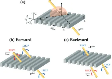
Figure 2.7 sketches a ultra-thin slab with thicknessLconsisted of periodic Ag/air bilayers. The
structure period isΛand the filling fraction of Ag layer is fAg. A monochromatic plane wave of
wavelengthλ0probes the slab forward and backward with incident anglesθandϕ. The incident
waves can be both left-handed circular polarised (LHCP) and right-handed circular polarised (RHCP),
[image:33.595.119.486.275.534.2]and also both forward and backward.
Figure 2.7: Geometry of the asymmetric transmission process. (a) Schematic view of the tilted plane wave (yellow arrow) impinging onto a ENZ slab consisted of Ag/air bilayers and the definition of the Cartesian coordinate and angular parameters. Propagation direction is defined as forward for thek(in)direction (b) and backward for the−k(in)direction (c).
The wave vector of the incident wavek(in)can be described as
k(in)=k(xin)ex+k(yin)ey+k(zin)ez=k0(sinθcosϕex+sinθsinϕey+cosθez) (2.13)
where superscript(in)represents incident wave, (ex,ey,ez) are the unit vectors in Cartesian
The dielectric response here is also described as Equation 2.2 and there are two forward waves
excited inside the slab, viz. the ordinary (o) and extraordinary (e) plane waves, whose longitudinal
wave vectors are
k(zo)=
k20⊥−(k2
x+k2y) (2.14)
k(ze)=
k2
0−(k2x ⊥ +k
2
y) (2.15)
At hyperbolic ENZ range where⊥≈0 (⊥ <0) and >0, the ordinary wave is evanescent (k(zo)=
−(k2
x+k2y)), whereas the extraordinary wave is a propagating mode and it can accumulate
the desired propagation phase even if the slab is ultrathin. Actually, the hyperbolic dispersion in the
ENZ regime leads to the large longitudinal wave vectors for extraordinary waves (k(ze)k0), thus
triggered the etalon resonances and enhance the asymmetric response of transmissions in forward
and backward directions[87].
To quantify the asymmetric transmission, we consider the linear and circular polarisation for the
optical wave.
First, for linear polarisation, TE(s) and TM(p), whose basis is ( es = −sinϕex+cosϕey,ep =
cosθcosϕex+cosθsinϕey−sinθez), the forward transmission matrix (−→Tl) is obtained by
⎛ ⎝E(pt)
Es(t)
⎞ ⎠=
⎛
⎝−→tpp −t→ps
−→ tsp −→tss
⎞ ⎠
⎛ ⎝E(pin)
Es(in)
⎞ ⎠=−→Tl
⎛ ⎝E(pin)
Es(in)
⎞
⎠ (2.16)
whereE(in)= (E(pin),Es(in))andE(t)= (E(pin),Es(in))are the incident and transmitted electric fields,
−→
tuv(u,v= p,s) means the matrix component of−→Tl.
As we consider the anisotropic slab, the cross-polarisation transmission coefficients are same and
nonzero, i.e.
−→
tps=−t→sp =0 (2.17)
Similarly, the forward transmission matrix (−→Tc) of left (+) and right (−) circular polarisations,
whose basis is ( e+= (ep+i es)/
√
2, e− = (ep−i es)/
√
2), can be described as
−→
Tc=
⎛
⎝−→t++ −→t+− −→ t−+ −→t−−
⎞
⎠ (2.18)
−→ t++= 1
2( −→ tpp+−→tss)
−→ t+−= 1
2( −→
tpp− −→tss−i2−t→ps)
−→ t−+= 1
2( −→
tpp− −→tss+i2−t→ps)
−→ t−−= 1
2( −→ tpp+−→tss)
(2.19)
In the situation of backward probing where the incident wave propagates along−k(in)direction,
the backward transmission matrices for linearly and circular polarised bases can be obtained based
on the reciprocal theorem[88]. Furthermore, the asymmetric transmissions for linear and circular
polarisations are characterised by the parameters
Δl =−t→sp
2
−←t−sp
2
=−t→sp
2
−−t→ps
2
(2.20)
Δc=−→t+−
2
−←−t+−
2
=−→t+−
2
−−→t−+ 2
(2.21)
Using Equations 2.17 and 2.20, we can obtainΔl =0, which means that the asymmetric
transmis-sion is not supported by linearly polarised waves.
From Equations 2.19 and 2.21, the asymmetric transmission parameter for circular polarised basis
is rearranged, shown as
Δc=2|Δt|t−→spsin(Δψ) (2.22)
whereΔt=−→tpp− −t→ss andΔψ=arg(Δt−t→ps∗).
Equation 2.22 shows that the asymmetric transmission for tilted circular polarised waves results
from both the linear polarisation asymmetric response (Δt=0) and the presence of the linear cross-polarisation conversion (−t→ps =0). These two factors are the natural characteristics of the uniaxial
medium. Therefore, the values ofΔtand−t→ps are the keys to achieving a dramatic enhancement of
the asymmetric transmission.
A specific Ag/air structure is demonstrated here to show the enhancement of the asymmetric
transmission in the AENZ regime. The parameters of the structure (Figure 2.7 (a)) areL=30 nm, fAg = 0.5 and θ = 60◦. The permittivity of Ag is obtained by Equation 2.1, where = 5, ωp =
Under the homogenised condition whereΛλ, effective permittivity of the Ag/air structure is obtained using EMT, i.e. Equations 2.2, 2.3 and 2.4, and the zero-permittivity point (Re(⊥) =0) locates atλ=0.4 μm, indicated in Figure 2.8 (a).
Figure 2.8 (b) illustrates the asymmetric transmissionΔcversusλand ϕ. The maximumΔc≈0.2
is obtained atλ=0.42 μm andϕ=45◦where⊥ =−0.14+i0.14 and=1.32+i0.01.
Figure 2.8: Numerical simulation results of the asymmetry transmissions in the ENZ slab sketched in Figure 2.7.[89] (a) Real part of⊥as a function ofλ(the shadow area indicates hyperbolic region). (b)Δcparameter as a function of ϕandλforθ=60◦andL=30 nm. (c) Comparison between the
asymmetric transmission evaluated with EMT (black solid line) and those predicted by the rigorous coupled-wave analysis for different values of the spatial periodΛ.
For the purpose of verifying the above results attained based on EMT and also discussing
the influence of spatial nonlocality on the considered asymmetric transmission, we use another
numerical method, namely the rigorous coupled-wave analysis technique[90], to calculate the
asymmetric transmissionΔc.
Figure 2.8 (c) exhibits the comparison between the asymmetric transmission evaluated with EMT
and those predicted by the rigorous coupled-wave analysis for different values ofΛ, atϕ=45◦and θ=60◦. The nonlocality impacts the results in the ENZ regime and it slightly reduces the value of theΔc. Therefore, the results of the rigorous coupled-wave analysis method initially prove that the
asymmetric transmission is purely related to the homogeneous structure response.
The work of this section has been published in the journal "Journal of Optics", see Reference[89].
We have demonstrated that the 1D ENZ slab can exhibit the asymmetric transmission of different
circularly polarised light which are typically shown in complex 2D and 3D chiral structures.
our investigation constitutes a fundamental step for the realisation of compact polarisation devices.
2.4
Emission enhancement on the ENZ substrate
Here, we discuss the emission enhancement of the condition where the light source (e.g. dipole or
nanoantenna) locate on top of an ENZ medium.
As ≈0, the refractive index (n) of the ENZ medium also approaches 0. Therefore, air is an optically denser medium comparing to the ENZ medium. Considering the situation where a light
beam propagates from a optically denser medium (e.g. air) to a optically thinner medium (e.g. ENZ
slab), the total reflection phenomenon will be launched where incident angle (θin) reaches critical
angle (θc). Based on Snell’s Law[80], theθcis determined when the transmitted angle (θt) reaches
90◦, asθc=arcsin(nntd), wherendandntare the refractive indices of the optically denser and thinner
media, respectively. At the interface between ENZ medium and air,nt=nENZ≈0 andnd=nair =1,
henceθc≈0, which means that the total reflection occurs at all incident angles.
Figure 2.9 sketched the air/substrate model with a plasmonic nanoantenna (light source) located
on top of the substrate at the interface[47]. The permittivity of substrate varies from positive (>1) through near-zero (≈0) to negative (<−1). When the light source is placed on top a substrate with > 1, such as dielectric materials with low loss, the emission is mainly scattered into the substrate (Figure 2.9 (a)). When the substrate is switched to ENZ medium, most emission energy
has been squeezed into the air direction (Figure 2.9 (b)), because the air is optically denser than the
substrate and thus the total reflection occurs. If the permittivity of the substrate decreasing down
to negative, the emission of the source propagating in the substrate part vanishes quickly (Figure
2.9 (c)), because of the high conductivity of the substrate for the electromagnetic fields[91], and this
Figure 2.9: Diagram of the emission distribution of light source located on top of substrates with different permittivities: >1 (a),≈0 (b) and<−1 (c)[47].
Hence, the emission will be enhanced due to the presence of the ENZ substrate, and this effect is
verified by our demonstration in Chapter 3.
In reality, we need to consider the complex refractive index (n) which consisted with the real
part (n) and imaginary part (n, the extinction coefficient), i.e.n=n+in. Similarly, the complex permittivity is=+i. Then, the real part of the refractive index is determined by permittivity as
n =
||+
2 (2.23)
where||=√2+2.
The optical loss of the medium (n) is also obtained
n=
|| −
2 (2.24)
By designing the ENZ structure using material with small , we can realise the emission enhancement with low optical loss. Meanwhile, the ENZ substrate can concentrate the emission
direction perpendicular to the interface due as the wave-front modification will be launched even
with the distances just in the size of several free-space wavelengths[47], as we discussed in Section
2.5
Summary
Based on EMT and Drude-Sommerfeld model, we can design, modify and manipulate the effective
permittivity of anisotropic and homogeneous structures and obtain the AENZ and IENZ media.
This ability motivates the applications of ENZ media in phase variation minimising and wave-front
modification. Additionally, the asymmetric transmission effect is enhanced in the ENZ regime. The
ENZ substrate is also capable of enhancing the emission of light sources with high directivity. Based
on these works, ENZ MMs open up important applications in the fields of sub-wavelength imaging,
emission modifying and optical sensing, etc. However, in the following chapters, I have only focused
on my works, which aims at the approaches to realising ENZ MMs and some other ENZ hybrid
Fabrication, characterisation of multilayer
ENZ structures and related emission
enhancement
This chapter demonstrates an approach to fabricate metal/dielectric multilayer ENZ structure using
e-beam evaporation method. The retrieval method to optically characterising the ENZ samples is
also explained in detail. Using this ENZ structure as substrate, we are able to enhance the emission
of gallium arsenide (GaAs) QDs.
The outline of this chapter starts with an overview of the nanotechniques used in the fabrication
of multilayer ENZ structures, before the explanation of the details of the fabrication process, typically
the e-beam evaporation. The optical characterisation of each unit layer and the multilayer structure
are also demonstrated here. Then, the numerical simulation and experimental verifying of the
emission enhancement on ENZ substrate are presented. The final section summarises with a
discussion of the influence of the fabrication and characterisation methods on the ENZ MMs for
further optical applications.
3.1
Overview
According to EMT, we realise the ENZ structure by layering materials with positive (dielectric)
and negative (metal) permittivity, with sub-wavelength thicknesses that are chosen so that the real
part of the effective permittivity crosses zero at the desired wavelength, e.g. visible range. The
deposition of each unit layers is implemented inside the chamber of an e-beam evaporator typically
Ag, Au and germanium (Ge)) and dielectric (e.g. SiO2and zinc selenide (ZnSe)) thin layers, with
high-accuracy thickness and ultra-high purity. This approach provides a way to realise the multilayer
ENZ structure in large scale and controllable thickness.
In this work, we also demonstrate a method to retrieve the permittivity of optical films, based on
Fresnel’s law[80]. This approach is able to determine the effective permittivity values of a given slab
by combining the thickness, transmission and reflection, without considering the other details inside
the structure. Using this method, we can characterise the optical properties of ENZ structures and
their unit layers.
Based on this ENZ platform, we also propose and demonstrate an approach to enhance the
emission properties of GaAs QDs at a specific wavelength range.
3.2
Fabrication
To achieve the ENZ condition at visible range with low loss, we design the multilayer ENZ structure
formed by unit layers of Ag and SiO2. In the visible regime, Ag with negative permittivity exhibits
lower loss than most noble metals[92, 93], and SiO2with positive permittivity shows good thermal
stability and also negligible optical loss. In the designed multilayer ENZ structure, unit layers have
sub-wavelength thicknesses to satisfy the requirement of EMT. Additionally, the thickness of the Ag
layer is required to be as lower as possible to reduce the optical loss of the whole structure. Therefore,
the thickness of Ag and SiO2unit layers are determined astm=6 nm andtm=60 nm, sketched in
Figure 3.1. In order to make the multilayer structure symmetry, the top and bottom layers are all
SiO2films with a thickness oftd/2. The substrates to hold the structure are square coverglass (Agar)
with side length of 24 mm and thickness of 200 μm.
Figure 3.1: Diagram of the multilayer ENZ structure consisted of Ag and SiO2unit layers.tmandtd
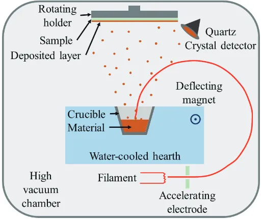
The multilayer metal/dielectric structure is fabricated using an e-beam evaporation approach.
The diagram of the e-beam evaporator (Edwards AUTO 306) is shown in Figure 3.2. The target
material (Ag or SiO2) was stored in a tungsten (W) crucible which held by a water-cooled hearth.
During the evaporation process, the target material was bombarded with a focused electron beam
(FEB) deflected by a magnet system, thus evaporated into gaseous particles and finally forming thin
layers when reached the substrate right above the crucible. Typically, the beam current was set at
about 45 μA for Ag and 6 μA for SiO2to reach an evaporation rate of 0.1 nm s−1. A quartz crystal
detector was used to monitor the evaporation rate and thickness. By modifying the tooling factor of
the detector, we could calibrate the thickness of deposited films. During the evaporation process, the
substrate holder was rotating all the time, around the axis perpendicular to its bottom surface, to
improving the smoothness of deposited layers. The whole evaporation process was performed in a
high-vacuum chamber with a base pressure of about 3×10⁻⁶mbar and a working pressure that less
[image:42.595.174.433.367.582.2]than 2×10⁻⁵mbar.
Figure 3.2: Diagram of the e-beam evaporator, formed with filament for generating electron beams, electrode for accelerating and focusing electron beams, magnet system for deflecting electron beams, W crucible for holding target materials, water-cooled system to accommodating the crucible, quartz crystal detector for monitoring evaporation rate, and the rotating holder of samples.
The e-beam evaporation approach can deposit large and uniform metal and dielectric thin films. The maximum size of the deposited film reaches 10 cm×10 cm, which is the size of the sample
holder. However, e-beam evaporation technique has some disadvantages. Because the evaporation