Innovative mid-infrared detector concepts
Sven Höfling
1,2, Andreas Pfenning
1, Robert Weih
1, Albert Ratajczak,
1Fabian Hartmann,
1Georg
Knebl,
1Martin Kamp,
1and Lukas Worschech
11
Technische Physik, Physikalisches Institut and Wilhelm Conrad Röntgen-Center for Complex
Material Systems, Universität Würzburg, D-97074 Würzburg, Germany
2
SUPA, School of Physics and Astronomy, University of St Andrews, St Andrews, KY16 9SS,
United Kingdom
ABSTRACT
Gas sensing is a key technology with applications in various industrial, medical and environmental areas. Optical detection mechanisms allow for a highly selective, contactless and fast detection. For this purpose, rotational-vibrational absorption bands within the mid infrared (MIR) spectral region are exploited and probed with appropriate light sources. During the past years, the development of novel laser concepts such as interband cascade lasers (ICLs) and quantum cascade lasers (QCLs) has driven a continuous optimization of MIR laser sources. On the other hand side, there has been relatively little progress on detectors in this wavelength range. Here, we study two novel and promising GaSb-based detector concepts: Interband cascade detectors (ICD) and resonant tunneling diode (RTD) photodetectors. ICDs are a promising approach towards highly sensitive room temperature detection of MIR radiation. They make use of the cascading scheme that is enabled by the broken gap alignment of the two binaries GaSb and InAs. The interband transition in GaSb/InAs-superlattices (SL) allows for normal incidence detection. The cut-off wavelength, which determines the low energy detection limit, can be engineered via the SL period. RTD photodetectors act as low noise and high speed amplifiers of small optically generated electrical signals. In contrast to avalanche photodiodes, where the gain originates from multiplication due to impact ionization, in RTD photodetectors a large tunneling current is modulated via Coulomb interaction by the presence of photogenerated minority charge carriers. For both detector concepts, first devices operational at room temperature have been realized.
Keywords: Interband Cascade Detector, Resonant Tunneling Diode, Mid-IR, Gas Sensing
1. INTRODUCTION
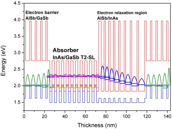
Just as interband cascade lasers (ICLs) the interband cascade detector (ICD) [1] makes use of the broken gap alignment of the two binaries GaSb and InAs. The conduction band of InAs is situated below the valence band of GaSb which allows for interband tunneling and thus cascading. An ICD stage is composed of three main parts as shown in the band structure in Figure 1. The short period InAs/GaSb superlattice (SL) works as absorption region for MIR radiation. The fact that the effective bandgap in the SL and thus the cutoff wavelength can be tuned via the SL-period introduces great design flexibility while only binary compounds have to be grown. Additionally the interband transition enables normal incidence detection. The absorber region is surrounded by a barrier and an electron relaxation region. On one side electrons are hindered from tunneling back to a previous cascade by an AlSb/GaSb electron barrier. This is because the upper level energy level in the absorption region is situated in the bandgap of GaSb. On the other side the AlSb/InAs electron relaxation region enables the transport of electrons to the InAs/GaSb interface that is used to connect the cascades in series. Electrons are transferred to the next stage through an interband tunneling process. The cascading scheme helps to overcome the strong coupling between responsivity and diffusion length which plays a major role especially at high temperature operation [2]. In a bulk material the diffusion length is typically shorter than the absorption depth which has a strong impact on the absorption efficiency. By cascading several absorption regions the total thickness of the structure can be designed longer than the diffusion length since the generated carriers only travel through one stage before entering the next one. This helps to improve the detectivity and the signal to noise ratio.
Invited Paper
Infrared Remote Sensing and Instrumentation XXIV, edited by Marija Strojnik, Proc. of SPIE Vol. 9973, 997306 · © 2016 SPIE · CCC code: 0277-786X/16/$18 · doi: 10.1117/12.2237270
Proc. of SPIE Vol. 9973 997306-1
a
1 gion 120 140 4.5 4.0 3.5 3.0 -Electron AISb /GaS 2.5 -2.0 1.5-0 21 barrier ìb Absorbe InAs /GaSI [i IO 40 Electr AISbIr
b T2-SL 60 80 Thickness 0ron relaxation reç
[image:2.612.147.440.100.320.2]/InAs
Figure 1: superlattic
The second tunneling dio 5] Resonant t electrical sign impact ioniza of photogene thousand, [1 realized on G spectral regio material syste materials that bandgap ener GaSb substra systems, and energies for M First GaSb/A for light sens studied by me
Band structur ce absorber reg
detector conc ode photodetec tunneling diod nals. [9–11] I ation, in RTD erated minority 10,11] at con GaAs or InP b ons, where for em is the sim t provide narr rgies and hete ate growth. [1
move it to a MIR light dete AlSb double ba sing up to a w eans of electri
re of one stag ion, the AlSb/G
cept for nove ctors. Besides des (RTDs) [6 In contrast to
photodetector y charge carr siderably sma based material
r example bot milar nano-inje rower bandgap
erostructure d 8] We therefo GaSb-based s ection. arrier resonan wavelength of ical transport a
ge of an interb GaSb - electron
el MIR-photo s being exploit
6–8] can act a o avalanche p rs a large tunn iers. [12–14] all operation l systems, whi th important t ector design. [ ps need to be designs is the
ore propose to system. Thus
nt tunneling di f = 2.76 µm
and photolum
band cascade d barrier and the
detectors disc ted as high-fre as low-noise a hotodiodes, w neling current
This allows f voltages. [14 ich allows for telecommunic [16,17] Never considered. S
so called ant o take the RT
exploiting bot
iodes with a n m have been r minescence me
detector (ICD). AlSb/InAs - el
cussed in this equency oscil and high-speed where the gai
is modulated for very high ,15] The maj r excellent lig cation wavelen rtheless, when Such a materia
timony or 6.1 TD principle a
th, high charg
nearby and lat realized. Thei easurements, r
The main pa lectron relaxatio
s work is tha llators and em d amplifiers o in originates
via Coulomb amplification jority of RTD ght sensing in
ngths are loca n pushing for
al system that 1 Å material as it is known ge-carrier amp
tice-matched ir electrical o respectively.
arts are the InA on region.
at of GaSb-b mitters in the T of small optic from multipli b interaction by n factors of se
D photodetec the visible or ated. Also bas longer wavele t provides a h
system, typic n from GaAs a
plification and
GaInAsSb ab ptical propert
As/GaSb -
based resonan THz range, [3–
ally generated ication due to y the presence everal hundred tors has been r near infrared sed on the InP ength regions huge variety o cally based on
and InP based d low bandgap
bsorption layer ties have been nt – d o e d n d P s, f n d p r n
Proc. of SPIE Vol. 9973 997306-2
10°
10 °,
Os
104
10'-10', 10',
10°.
10e
+ `
1
I+I I I IIIil, I IIÌ ill
-4000 -2000 0 2000 4000
40) (arcsec)
10°=
3.0 s
104
10'=
10',
10',
11 III'I
10° - 7 IÌI ÌI I 111111
-4000 -2000
10°
10°
4)
= 10'
10'
10°
2.1 s
100
10°
10°
100
10°
:::1I llI
liluiil
¡hi lid
910 2000 4000 -4000 -2000 0 2000 4000
I IIII1IIIü -4000 -2000 0
4w(arcsec)
Y Ì IIIII.
hill
2000 4000
6.0 s
40) (arcsec) dw (artsec)
2. INTERBAND CASCADE DETECTORS
[image:3.612.119.494.316.594.2]Since the quality of the InAs/GaSb-SL is of major importance for the performance of the final device careful optimization was done regarding the MBE growth by growing a variety of test samples at different growth conditions. The structures were grown in an Eiko MBE reactor equipped with cracker cells for both As and Sb. The cracking regions of the cracking cells were operated at 950°C and 1000°C, respectively, to ensure efficient cracking of As and Sb. As the structure is grown on GaSb-substrates, the smaller lattice constant of InAs would introduce tensile strain which might result in defect formation or relaxation once the SL reaches a certain thickness. Thus the mean SL lattice constant should match the one of the substrate which was achieved by enforcing InSb interfaces. The 30 period SL test structures were grown at a substrate temperature of 430°C and had a nominal SL-period of 4.56 nm (2.12 nm InAs / 2.44 nm GaSb). After each GaSb layer a 2s soak time under Sb flux was applied while the duration of the Sb soak time after the InAs layer was varied between 0 and 6 s. In Figure 2: high resolution X-ray diffraction (HR-XRD) measurements of various samples with soak times of 0, 2.1, 3.0 and 6.0 s are shown. The high frequency Pendellösung fringes indicate high material quality for all samples. It can be seen that for the sample with no applied Sb soak time after the InAs layer the 0th order SL-peak occurs at the right side of the substrate which is a result of tensile strain. With increased soak time the peak shifts further to the left till the SL overall strain becomes compressive due to the InSb – like interfaces. At a soak time of 2.1 s the mean lattice constant of the SL coincides with the one of the substrate. It should be mentioned that the shift of the SL-peak does not vary linearly with the soak time due to a saturation of the Sb for As exchange reaction [19].
Figure 2: HR-XRD measurement of 30 period InAs/GaSb test samples. The Sb soak time after the InAs layers was varied between 0 s and 6 s. Strain compensation was achieved for a soak time of 2.1 s.
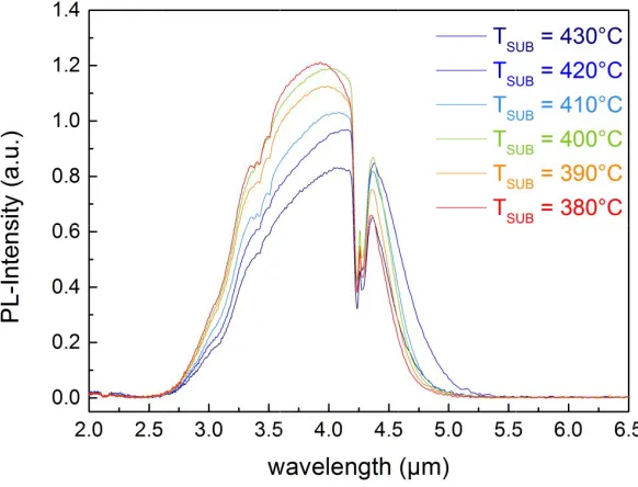
Furthermore the influence of the growth temperature (380°C – 430°C) on the optical properties of the SL was investigated. Due to the temperature dependence of the Sb for As exchange reaction the 0th order peak of the SL shifted
slightly towards smaller angles when the substrate temperature was decreased. No compensation by adjusting the soak time was done in this series of samples. In Figure 3 room temperature photoluminescence (PL) measurements are shown for all samples. The half maximum on the low energy side coincides with the calculated room temperature cutoff
Proc. of SPIE Vol. 9973 997306-3
UB = 430°C
UB = 420°C
UB = 410°C
UB = 400°C
UB = 390°C
UB = 380°C
5 6.0 6 t5
1.4 1.2 1.0 0.8 0.6 0.4 0.2 0.0
20
2.5/
3.0 3.55 410 41E
iavelength
Ts Tsi Ts, Ts, TsiIs
5 5.0 5!:
(pm)
[image:4.612.149.440.199.421.2]wavelength o result of hig pronounced P wavelengths change in gro sample grown optimum gro might suffer f
Figure 3: increases
Based on the incorporated the range from Si3N4 and SiO
characteristic density is as l in the literatu absorption fe explains the s
of 4.5 µm. A m gher interface Pendellösung
is observed f owth rate wit n at the lowe owth temperat from low grow
Room temper monotonically
previously sh 5 stages with m 10 µm to 4 O2 was sputte
cs of devices w low as 5.2 x 1 ure [20,21]. In eatures of H2O
slope on the sh
monotonic inc quality whic fringes in HR for low growt th substrate te est temperatur
ture for an en wth temperatu
rature PL meas when the grow
hown optimiz 90 SL period 400 µm were ered for sidew with different 10-4 A/cm2 for
n Figure 4 (b Oand CO2. Th
hort waveleng
crease in PL in ch is also co R-XRD measu th temperatur emperature. T re shows the ntire ICD stru ure.
surements of S wth temperature
zations an ICD ds in each stag
defined using wall passivatio diameters me r the device w b) the spectral he curve is no gth side below
ntensity with d onfirmed by h urements. Be res. This indic Taking the PL best results. N ucture since th
SL samples gro is lowered.
D structure wa ge. From the g
g optical litho on and Ti/Pt/A easured at roo with a diamete l response cu ot corrected f w 2.5 µm.
decreasing gro higher intensi sides the incr cates a smalle L intensity as Nevertheless he quality of
own at differen
as grown by M grown wafer c ography and d Au-contacts w
m temperatur er of 400 µm urve of the de for the intensi
owth temperat ity of the SL rease in inten er SL period
a measure o this does not
the Al-contai
nt substrate tem
MBE on a p-G circular mesas dry etching. A were evaporate
re are shown. which is com evice is show ity distribution
ture was obse L satellite pea
sity a shift to and could be f structural q
necessarily h ining parts of
mperatures. Th
GaSb substrat s with differen Afterwards a c
ed. In Figure At -0.04 V th mparable to val wn. One can c n of the MIR
rved. This is a aks and more owards shorter e a result of a quality the tes
have to be the f the structure
e intensity
te. The design nt diameters in ombination o
4 (a). the IV he dark curren lues published clearly see the source which a e r a st e e n n f -nt d e h
Proc. of SPIE Vol. 9973 997306-4
Current density (A/cm2) N
...
Ñ
ó ó ó
...ó ....ó ....ó ...o
. ... ...
1....1.
- Diameter
-400um
--200um
- 100 um - 50 um-25 um
-10um
-1.5
\
6
Response (a.u.)
v
fie 5 5 0' 20 2.5
(b)
3.5 4.0 ongth (pm)-T = 20°C
I 4.5
(a)
00 Figure 4: temperatu An example based on the temperature. exceeding 3.3 applied bias dark (black livoltage equa
absorption re where they a characteristic Figure 5: telecomm profile un characteri GaInNAs
(a) Room tem ure spectral resp
of an RTD p GaAs materi With these d 30 10 . [15 voltage and ine), and unde
tion. [23] Wh gion. The thu accumulate an cs shifts towar
Example of des munication light nder an applie istics in the dar absorption reg
mperature curren ponse of the ICD
3. RESO
photodetector ial system an iodes, sensitiv 5] Figure 5 (a)
d under illum er illumination hen the RTD usly photogene nd induce an a rds lower volta
sign and workin sensing based ed positive bi rk (black line) gion and drift to
nt - voltage cha D (not normaliz
ONANT TUN
including des d was design vities of abov ) shows the sc mination. Figu
n (red line), ca is illuminated erated holes d additional vol ages. [24]
ng principle of on the GaAs m ias voltage
and under illu owards the AlG
aracteristics of zed for the inten
NNELING B
sign and work ned for highly
ve 30 kA/W h chematic cond re 5 (b) show alculated after d, incident ph drift towards t ltage drop acr
a resonant tunn material system. and under ill umination (red l GaAs/GaAs reso
the MIR ICD nsity distributio
BASED DET
king principle y sensitive tele have been rea duction (CB) ws a typical R r Schulman’s hotons create the AlGaAs/G ross the RTS.
neling diode (R (a) Schematic lumination. (b) line). Under ill onant tunneling
for different m on of the broadb
TECTORS
e is provided ecommunicati alized, [11,22] and valence b RTD current-v
model for a p
electron-hole GaAs resonant . [12,13] As a
RTD) photodetec conduction (CB ) Sketch of t lumination, hol g structure (RTS
mesa diameters. band MIR sourc
in Figure 5. ion light dete ] with amplifi band (VB) pr voltage charac
physics-based
pairs within t tunneling str a result, the c
ctor for room te B) and valence the RTD curre les are created S) where they a
(b) Room ce).
The device is ection at room ication factors rofile under an cteristic in the
d RTD current the GaInNAs ructure (RTS) urrent-voltage emperature band (VB) ent-voltage within the accumulate s m s n e -s ), e
and induce an additional voltage drop across the RTS. As a result,, the current-voltage characteristics under illumination shifts towards lower voltages.
Proc. of SPIE Vol. 9973 997306-5
In order to de on the GaSb profiles of th structure. The tunneling stru second AlSb GaInAsSb ab mid-infrared the SEM ima identified. Ov no defects. F corresponding corresponds t light detectio windows cov Figure 6: underlying represents tunneling n-type Te sandwichi Ga0.76In0.2
(b) Room line).
esign and fabr material syste he proposed R
e proposed sa ucture consist barrier is fol bsorption laye spectral regio age, dark cont verall, the SEM Figure 6 (b) g cut-off wav to a cut-off w n within the w vers important
(a) Conductio g picture is a s layers with h structure with e-doped GaSb. ing a 6 nm GaS
24As0.20As0.80. T
m temperature b
ricate RTD ph em. Figure 6 ( RTD photodete mple was real ts of 20 nm G llowed by a 1 er with a dopi on. The struct trast correspo M image conf
shows the c velength. The wavelength of
wavelength ra absorption lin
on and valence scanning elect high Al concen
a nearby and la . The double Sb quantum we The SEM image bandgap energy
hotodetectors (a) shows the ector underlai
lized by MBE GaSb, and two
0 nm GaSb b ng concentrat ture is finalize nds to region firms excellen calculated ban bandgap ener
= 2.76 µ ange between nes of for exam
e band profile tron microscopy
ntration. The R attice-matched
barrier resonan ell. The lattice-e confirms lattice-exclattice-e y versus crystal
for the mid-in conduction (r in with a scan E growth on a o 4 nm AlSb b
buffer layer. A tion of = 2 ed by 300 nm ns with high A nt crystal qual ndgap energy rgy of the GaI µm (see also = 1.7 µm mple water an
s of the mid-i y image of the RTD photodete absorption laye nt tunneling s -matched absorp ellent crystal qu l position (blac
nfrared spectr red solid line) nning electron an n-type dope
barriers sandw A slightly n-ty 2.0 10 cm m of highly do Al concentrati lity with high y profile (bla InAsSb absorp
Figure 7 (a)). (cut-off wave nd carbon diox
infrared resona e grown semic ector consists o er. Top and bot structure is ma ption layer is f uality with high ck line) and the
al region, we ) and valence n microscopy
ed GaSb-subst wiching a 6 nm
ype doped an m-3 allows for
oped GaSb wi on. The two A hly uniform Al ack line) at r
ption layer is . Hence, the R elength of GaS
xide.
ant tunneling d conductor layer
of an undoped ttom contact lay ade of two 4 formed by the q hly uniform AlS e corresponding
propose an ap band (light b (SEM) image trate. The intr m GaSb quant nd 250 nm wi light absorpt ith = 3.0 AlSb barriers lSb barriers, i room tempera = 0.451 RTD will be s
Sb) and = 2
diode photodet r structure. Dar d double barrie yers are formed nm thick AlS quaternary sem Sb barriers and g cut-off wavel
pproach based blue solid line e of the grown
rinsic resonan tum well. The ide quaternary ion within the 10 cm-3. In
can be easily interfaces, and ature, and the 1 meV, which suited best for 2.76 µm. This
tector. The rk contrast er resonant d by highly Sb barriers miconductor interfaces. length (red d ) n nt e y e n y d e h r s
Proc. of SPIE Vol. 9973 997306-6
Figure 7 (a) s absorption lay the position o energy of matched to G spheres. GaS 0.24 the band
Figure 7: peak posi energy sid meV. (b) matched g meV. CB
Figure 8 de temperatures. found with a µA/µm2 at
current bistab
Figure 8: Helium (
shows the exp yer as solid re of the half-max = 450 me GaSb after Re b CB minimu dgap energy is
(a) Experiment tion is located de and located
Energy positio growth conditio
minimum and
epicts the ex . The j(V)-cha
peak current = 1.88 V. Th bility is of intr
Current densi
= 4.2 K, blu
perimental roo ed line. The P ximum at the eV. Figure 7 ( f. [25]. The C um and VB m s = 451
tal room tempe
at = 2.62 µm
at = 2
on of the GaInA on as a functio
VB maximum
xperimental R aracteristic fo -density of he correspond rinsic nature (s
ity-voltage (j(V ue spheres); su
om temperatur PL peak posit
low-energy si (b) shows a c CB minimum maximum are meV, which p
erature photolum m. The cut-off
2.76 µm. The AsSb conductio on of mole-frac are calculated a
RTD current or = 4.2 K
= 3.73 µ ding peak-to-v
see Ref. [26,2
V)-) characteris ubmerged in liq
re ( = 20 °C tion is located ide and locate alculation of is shown as r indicated by perfectly fits t
minescence (PL wavelength is g cut-off wavelen on band (CB) m ction compositio according to Re
density-volta is shown as b µA/µm2 at =
valley current 27]). Other tha
stics measured quid nitrogen (
C) photolumin d at = 2.62 ed at = 2.
the band extr red spheres, a the dashed re the PL measur
L) spectrum of given by the po ngth correspon minimum and v on x. At = 0
ef. [25].
age (j(V)-) c blue spheres. = 1.92 V, and
ratio is an that, there
at three differ ( = 77 K, gr
nescence (PL) µm. The cut-76 µm, which rema of the qu and the VB m
ed and black rement.
the GaInAsSb osition of the h nds to a bandga valence band (V
0.24 the bandga
characteristics A well-prono d a valley cur = 11.3. Acco is little literatu
rent temperatur reen spheres); a
spectrum of -off waveleng h corresponds
uaternary GaI maximum is sh lines, respect
absorption lay half-maximum a
ap-energy of VB) maximum
ap energy is
s taken at th ounced curren
rrent density o ording to Jim
ure on that top
res: submerged and at room te
the GaInAsSb gth is given by to a bandgap InAsSb lattice hown as black tively. At =
er. The PL at the
low-= 450
for
lattice-= 451
hree differen nt bistability is
of = 0.33
enez et al, the
pic.
d in liquid emperature b y -e k = nt s 3 e
( ≅ 295 K, red spheres). Well-pronounced current resonances can be observed at = 4.2 K and = 77 K with
peak-to-valley current ratios of = 11.3 and = 7.5, respectively. At room temperature, resonant tunneling cannot be observed.
Proc. of SPIE Vol. 9973 997306-7
When increasing the temperature up to = 77 K (green circles), the peak current density decreases down to = 3.38 µA/µm2, whereas the valley current density increases to = 0.45 µA/µm2, with = 7.5. Decrease of peak
and increase of valley current density with increasing temperature can be attributed to two different mechanisms. On the one hand side, at higher temperatures increased phonon scattering reduces the number of electrons that can tunnel resonantly, and increases the number of electrons contributing to non-coherent transport. On the other hand, increasing the temperature leads to a depopulation of electrons in the GaSb Γ-valley, while increasing the electron population of the L-valley states. Hence, less electrons can contribute to tunneling via the Γ-Γ tunneling path. [28] At room temperature, no region of negative differential conductance, and therefore no resonant tunneling can be observed. We are currently investigating different approaches on how to improve the electrical transport properties of GaSb-based resonant tunneling diodes at room temperature. [29]
4. CONCLUSIONS
Two promising, novel and alternative detector concepts for the MIR region are demonstrated. ICDs combine the advantages of conventional type-II SL-detectors with the cascading scheme of ICLs. By applying proper soak times during the InAs/GaSb-SL growth the mean lattice constant of the SL was matched to the GaSb substrate. Furthermore a series of samples under variation of the substrate temperature was grown. The highest room temperature PL intensity was observed for the sample grown at the lowest substrate temperature (380°C). Finally a full ICD structure was grown and processed into circular detector devices operational at room temperature. The cut off wavelength was around 4.5 µm. Additionally a resonant tunneling diode photodetector with cut-off wavelength at = 2.76 µm is presented. It is based on an AlSb/GaSb double barrier resonant tunneling structure with a nearby and lattice-matched GaInAsSb-absorption layer. First results are promising, but indicate that for room temperature operation further approaches to improve room temperature resonant tunneling need to be considered.
ACKNOWLEDGEMENTS
The authors are grateful for financial support by the state of Bavaria, the German Ministry of Education and Research (BMBF) within the national project HIRT (FKZ 13XP5003B). Expert technical assistance by M. Emmerling and A. Wolf is gratefully acknowledged.
Proc. of SPIE Vol. 9973 997306-8
REFERENCES
1. R. Q. Yang, Z. Tian, Z. Cai, J. F. Klem, M. B. Johnson, and H. C. Liu, "Interband-cascade infrared photodetectors with superlattice absorbers," J. Appl. Phys. 107, 054514 (2010).
2. P. Martyniuk, J. Antoszewski, M. Martyniuk, L. Faraone, and A. Rogalski, "New concepts in infrared photodetector designs," Appl. Phys. Rev. 1, 041102 (2014).
3. T. Maekawa, H. Kanaya, S. Suzuki, and M. Asada, "Oscillation up to 1.92 THz in resonant tunneling diode by reduced conduction loss," Appl. Phys. Express 9, 024101 (2016).
4. S. Suzuki, M. Asada, A. Teranishi, H. Sugiyama, and H. Yokoyama, "Fundamental oscillation of resonant tunneling diodes above 1 THz at room temperature," Appl. Phys. Lett. 97, 33–36 (2010).
5. M. Feiginov, H. Kanaya, S. Suzuki, and M. Asada, "Operation of resonant-tunneling diodes with strong back injection from the collector at frequencies up to 1.46 THz," Appl. Phys. Lett. 104, (2014).
6. R. Tsu and L. Esaki, "Tunneling in a finite superlattice," Appl. Phys. Lett. 22, 562 (1973).
7. L. L. Chang, L. Esaki, and R. Tsu, "Resonant tunneling in semiconductor double barriers," Appl. Phys. Lett. 24, 593 (1974).
8. G. Haddad, P. Mazumder, and J. N. Schulman, "Resonant tunneling diodes: models and properties," Proc. IEEE
86, 641–660 (1998).
9. B. Romeira, L. M. Pessoa, H. M. Salgado, C. N. Ironside, and J. M. L. Figueiredo, "Photo-detectors integrated with resonant tunneling diodes.," Sensors (Basel). 13, 9464–82 (2013).
10. W. Wang, Y. Hou, D. Xiong, N. Li, W. Lu, W. Wang, H. Chen, J. Zhou, E. Wu, and H. Zeng, "High
photoexcited carrier multiplication by charged InAs dots in AlAs⁄GaAs⁄AlAs resonant tunneling diode," Appl. Phys. Lett. 92, 023508 (2008).
11. A. Pfenning, F. Hartmann, F. Langer, S. Höfling, M. Kamp, and L. Worschech, "Cavity-enhanced resonant tunneling photodetector at telecommunication wavelengths," Appl. Phys. Lett. 104, 101109 (2014).
12. P. England, J. E. Golub, L. T. Florez, and J. P. Harbison, "Optical switching in a resonant tunneling structure," Appl. Phys. Lett. 58, 887 (1991).
13. P. W. Park, H. Y. Chu, S. G. Han, Y. W. Choi, G. Kim, and E.-H. Lee, "Optical switching mechanism based on charge accumulation effects in resonant tunneling diodes," Appl. Phys. Lett. 67, 1241 (1995).
14. A. Pfenning, F. Hartmann, M. Rebello Sousa Dias, F. Langer, M. Kamp, L. K. Castelano, V. Lopez-Richard, G. E. Marques, S. Höfling, and L. Worschech, "Photocurrent-voltage relation of resonant tunneling diode
photodetectors," Appl. Phys. Lett. 107, 081104 (2015).
15. A. Pfenning, F. Hartmann, F. Langer, M. Kamp, S. Höfling, and L. Worschech, "Sensitivity of resonant tunneling diode photodetectors," Nanotechnology 27, 355202 (2016).
16. O. G. Memis, A. Katsnelson, S. C. Kong, H. Mohseni, M. Yan, S. Zhang, T. Hossain, N. Jin, and I. Adesida, "A photon detector with very high gain at low bias and at room temperature," Appl. Phys. Lett. 91, 6–9 (2007). 17. V. Fathipour, S. J. Jang, I. H. Nia, and H. Mohseni, "Impact of three-dimensional geometry on the performance
of isolated electron-injection infrared detectors," Appl. Phys. Lett. 106, 021116 (2015).
18. H. Kroemer, "The 6.1 family (InAs, GaSb, AlSb) and its heterostructures: a selective review," Phys. E Low-dimensional Syst. Nanostructures 20, 196–203 (2004).
19. M. Losurdo, P. Capezzuto, G. Bruno, A. S. Brown, T. Brown, and G. May, "Fundamental reactions controlling anion exchange during mixed anion heterojunction formation: Chemistry of As-for-Sb and Sb-for-As exchange reactions," J. Appl. Phys. 100, 013531 (2006).
20. Z.-B. Tian, T. Schuler-Sandy, and S. Krishna, "Electron barrier study of mid-wave infrared interband cascade photodetectors," Appl. Phys. Lett. 103, 083501 (2013).
Proc. of SPIE Vol. 9973 997306-9
21. Zhao-Bing Tian and S. Krishna, "Mid-Infrared Interband Cascade Photodetectors With Different Absorber Designs," IEEE J. Quantum Electron. 51, 1–5 (2015).
22. A. Pfenning, F. Hartmann, F. Langer, M. Kamp, S. Höfling, and L. Worschech, "Cavity-enhanced AlGaAs/GaAs resonant tunneling photodetectors for telecommunication wavelength light detection at 1.3 μm," in Proc. SPIE
9608, Infrared Remote Sensing and Instrumentation XXIII, M. Strojnik Scholl and G. Páez, eds. (2015), Vol.
9608, p. 960810.
23. J. Schulman, H. J. De Los Santos, and D. H. Chow, "Physics-based RTD current-voltage equation," IEEE Electron Device Lett. 17, 220–222 (1996).
24. I. J. S. Coêlho, J. F. Martins-Filho, J. M. L. Figueiredo, and C. N. Ironside, "Modeling of light-sensitive resonant-tunneling-diode devices," J. Appl. Phys. 95, 8258 (2004).
25. K. Shim, "Composition dependence of band alignments in Ga[sub x]In[sub 1−x]As[sub y]Sb[sub 1−y] heterojunctions lattice matched to GaSb and InAs," J. Appl. Phys. 114, 203703 (2013).
26. J. Jimenez, E. Mendez, X. Li, and W. Wang, "Intrinsic bistability by charge accumulation in an L-valley state in GaSb-AlSb resonant-tunneling diodes," Phys. Rev. B 52, (1995).
27. J. Jimenez, E. Mendez, X. Li, and W. Wang, "Resonant tunneling and intrinsic bistability in GaSb-based double barrier heterostructures," Solid. State. Electron. 40, 583–584 (1996).
28. J. L. Jimenez, X. Li, and W. I. Wang, "Resonant tunneling in AlSb-GaSb-AlSb and AlSb-InGaSb-AlSb double barrier heterostructures," Appl. Phys. Lett. 64, 2127 (1994).
29. A. Pfenning, G. Knebl, F. Hartmann, R. Weih, A. Bader, M. Emmerling, S. Höfling, and L. Worschech, "In Preparation: Room temperature operation of GaSb-based resonant tunneling diodes due to enhanced prewell injection," (2016).
Proc. of SPIE Vol. 9973 997306-10