Self-assembly of polystyrene-
block
-poly(4-vinylpyridine) block copolymer on molecularly
functionalized silicon substrates: fabrication of
inorganic nanostructured etchmask for lithographic
use
†
C. Cummins,abD. Borah,abcS. Rasappa,abcA. Chaudhari,abcT. Ghoshal,abc
B. M. D. O'Driscoll,abP. Carolan,abN. Petkov,abJ. D. Holmesabcand M. A. Morris*abc
Block copolymers (BCPs) are seen as a possible cost effective complementary technique to traditional lithography currently used in the semiconductor industry. This unconventional approach has received increased attention in recent years as a process capable of facilitating the ever decreasing device size demanded. Control over microdomain orientation and enhancing long range order are key aspects for the utility of BCPs for future lithographic purposes. This paper provides an efficient route for the fabrication of highly ordered nanostructures suitable for such application. We investigate the significant effect of surface treatment regarding the self-assembly process of polystyrene-block-poly(4-vinylpyridine) (PS-b-P4VP) by employing an ethylene glycol layer, producing well defined perpendicular P4VP cylinders with long range order over large surface areas. Nanopores are generated through surface reconstruction using a preferential solvent, which allows for the incorporation of an inorganic moiety. Treatment of this pattern with UV/Ozone leads to formation of well-ordered iron oxide nanodots with a pitch of26 nm. Furthermore, high aspect ratio silicon nanopillars result following pattern transfer (using Ar/O2).
Introduction
In an effort to enable the desired feature size of future elec-tronics, block copolymers (BCPs) have been the focus of intense research for the past decade, as outlined in numerous reviews.1–6BCPs now offer a promising alternative to the
tradi-tional‘top down’ fabrication methods due to their processing advantages as well as from an economic standpoint. Owing to diffraction limits, issues with lithography methods have been well documented, as the semiconductor industry now seek a robust high throughput approach. The exibility offered through the self-assembly of BCPs make these materials ideal candidates for a wide range of applications and are not solely limited to lithography. However, paramount to their success in the electronicseld is to produce high quality structures with long range order which possess few defects aer pattern
transfer.7,8 BCPs consist of two monomer components that
differ both physically and chemically and when microphase separated give rise to fascinating architectures. One such useful morphology is hexagonally packed cylinders, whereby when the minority block is removed or swollen creates nanopores which can be utilized for the deposition of metal nanoparticles (NPs). Smaller domain dimensions can be produced by lowering the molecular weight of the constituent BCP components and these tuneable characteristics highlight the importance of BCPs in the future allowing for the development of ultra-high density storage media.
Dewetting is a major problem encountered with BCPs which prevents pattern formation, limits correlation length and leads to defects. Altering surface energies plays a signicant role in controlling both wetting layer and morphologies of BCPs.9–11
Polystyrene-block-polymethylmethacrylate (PS-b-PMMA) has been one of the most intensely studied BCPs to date, and various methodologies have been employed to control self-assembly. In asymmetric PS-b-PMMA, where PMMA is the minority block, the PMMA block has a preferential interaction with the oxide layers on the silicon substrate, and thus leads to in plane cylinders. To overcome this, the generation of cylinders normal to the surface has been allowed through the use of aDepartment of Chemistry, University College Cork, Cork, Ireland. E-mail: m.morris@
ucc.ie; Fax: +353 214274097; Tel: +353 214902180
bTyndall National Institute, Lee Maltings, Prospect Row, Cork, Ireland
cCentre for Research on Adaptive Nanostructures and Nanodevices (CRANN), Trinity College Dublin, Dublin 2, Ireland
†Electronic supplementary information (ESI) available. See DOI: 10.1039/c3tc31498g
Cite this:J. Mater. Chem. C, 2013,1, 7941
Received 31st July 2013 Accepted 19th October 2013
DOI: 10.1039/c3tc31498g
www.rsc.org/MaterialsC
Materials Chemistry C
PAPER
Published on 22 October 2013. Downloaded by Trinity College Dublin on 11/12/2014 11:02:50.
random copolymer brushes to ‘neutralize’ the surface,12,13as
well as PS-OH brushes to modify surface energy of the silicon substrate.14 Recently Kim et al. have implemented a similar
methodology by adding PS-OH homopolymer to a BCP poly-styrene-block-polyethyleneoxide (PS-b-PEO) solution resulting in highly ordered microdomains with a reduced process time in comparison to long annealing periods required for usual substrate chemistry modications.15With regard to
polystyrene-block-poly(4-vinylpyridine) (PS-b-P4VP), control over micro-domain orientation has previously been demonstrated by hydrogen bonding small molecules such as 3-PDP, HABA and PBA to P4VP.16–20These routes typically take a number of days
for hydrogen bonding to successfully take place, adding to the complexity of the overall process.
A fundamental challenge for BCPs applicability for inte-grated circuit integration is the successful transfer of the resulting pattern from the microphase separated BCP to the underlying substrate. To ensure that the pattern is transferred properly etch contrast is required. This can be done by wet etching the BCP, so the minority block is removed or through surface reconstruction whereby nanopores are also produced aer exposure to a preferential solvent that induces swelling. Alternatively, plasma assisted etching (reactive ion etching (RIE) or inductively coupled plasma (ICP)), also known as dry etching, is a powerful tool for the selective etch of a minor component and etch directionality leads to ideal templates for pattern transfer as detailed in recent etch studies by Borahet al.21,22
To generate highly ordered silicon nanostructures with few defects a hard mask (such as Fe2O3) can also be employed, fabricated using the minority block removal/swelling previously detailed and then followed by the addition of a metal complex. Surface reconstruction has been demonstrated in PS-b-P4VP systems using a preferential solvent like ethanol,23,24and has
been reported in PS-b-PMMA BCPs using acetic acid.25 The
resulting nanopores allow for the deposition of various particles with wide ranging functions. With PS-b-P4VP, NP inclusion can be done either by depositing the NPs aer the self-assembly process or inclusion of the desired ratio of NP to the diblock copolymer solution before spin coating. For example, well-ordered micelle and cylindrical microdomains have been reported in PS-b-P4VP BCPs for metal inclusion to fabricate arrays of iron nanocatalyts,26 copper nanocatalyts,27 titania
NPs,28and iron platinum NPs.29
Herein, we describe a simple surface modication method (having a short processing time,1 h)–using a silicon oxide surface functionalized with an ethylene glycol layer and detail its subsequent effects for controlling the self-assembly process in asymmetric PS-b-P4VP as well as increasing surface coverage of the resulting morphology through solvent annealing. This increased surface coverage have benecial implications for transistor devices but also for other electronic devices such as passive on-chip capacitors whose storage capacity is dependent on area.30Our investigation also
high-lights the role that temperature has in producing highly oriented and well-ordered patterns. Using the surface recon-struction strategy which created a nanoporous template we
deposited an iron nitrate ethanol solution that was immedi-ately followed by UV/Ozone exposure to remove the polymer matrix surrounding the nanodot array. Signicantly we have shown that this BCP system with a hard mask led to a greater depth prole following pattern transfer.
Experimental
Materials
Planar substrates used were highly polished single-crystal siliconh100iwafers (p-type) with a native oxide layer of2 nm. No attempt was taken to remove the native oxide of a few nm depths. Polystyrene-block-poly(4-vinylpyridine) was purchased from Polymer Source, Inc., Canada, with a molecular weight of
Mn¼33.5 kg mol1(MnPS¼24 kg mol1;MnP4VP¼9.5 kg mol1,
fPS¼0.70), a polydispersity (Mw/Mn) of 1.10 (where,MnandMw are number average and weight average molecular weights) and was used without further purication. Iron(III) nitrate
non-ahydrate (Fe2(NO3)3$9H2O), ethylene glycol (EG, CH2(OH) CH2(OH), 95.0%), toluene (99.8%, anhydrous), tetrahydrofuran (THF) (99.8%, anhydrous), ethanol (dehydrated, 200 proof), acetone (99.0%, anhydrous), iso-propanol (IPA) (99.0%, anhy-drous), sulphuric acid (98.0%) and hydrogen peroxide (30.0%) were purchased from Sigma-Aldrich and used without further purication unless otherwise stated. De-ionized (DI) water was used wherever necessary.
Substrate cleaning, activation and modication with EG
Substrates were cut into 2.0 cm2pieces and then degreased by ultrasonication in acetone and IPA solutions for 5 min each, dried in owing N2gas and baked for 2 min at 393 K in an ambient atmosphere to remove any residual IPA. This was fol-lowed by cleaning in a piranha solution (1 : 3 v/v 30% H2O2: H2SO4) (Caution! May cause explosion in contact with organic material!) at 363 K for 60 min, rinsed with DI water (resistivity$18 MUcm1) several times, acetone, ethanol and dried under N2 ow. Piranha activation removes any organic contaminant, greases and creates hydroxyl groups on the silicon substrates. Solution of ethylene glycol (EG) 5% (v/v) was prepared in ethanol and was stirred at room temperature (288 K) for 2 h to ensure complete mixing. The hydroxylated substrates (by piranha solution as mentioned above) were immediately coated with ethylene glycol by spin-coating (P6700 Series Spin-coater, Speciality Coating Systems, Inc., USA) at 1000 rpm for 30 s. Samples were air dried at room temperature (288 K) for 30 min, washed with absolute ethanol and then dried under a stream of nitrogen. Films survived repeated rinses in ethanol as observed by XPS and FTIR.
BCPlm preparation and solvent anneal
The polymer was dissolved in a toluene : THF (80 : 20) mixture to yield 0.5 wt% solution and lestirring for 12 h to ensure complete dissolution. BCPlms were prepared by spin coating the polymer solution onto the substrates at 3000 rpm for 30 s. Following deposition, the PS-b-P4VP generated thinlms were exposed to a saturated THF environment at different temperaturesviz., 40C,
50 C and 60 C. Solvent annealing was carried out in the conventional manner with a small vial containing 8–10 ml of annealing solvent placed inside a glass jar (150 ml) with BCP sample for different time periods. Samples were removed from the glass jars aer the desired anneal time and allowed to evaporate the trapped solvent at ambient conditions.
BCPlm reconstruction with ethanol
Surface reconstruction was carried out by immersing the solvent annealed thinlm in ethanol for 20 minutes. Aer this immersion period, the sample was removed and dried under nitrogenow.
This provided enough time for swelling of the P4VP domains to enable reconstruction of a nanoporouslm for subsequent deposition of iron nitrate solution.
Iron oxide nanopattern development
Fe2(NO3)3$9H2O solution of 0.3 wt% was prepared in ethanol and spin-coated onto the ethanol reconstructed lm at 3000 rpm for 30 s. UV/Ozone treatment was used to oxidize the precursor and remove polymer. Samples were UV/Ozone treated in a UV/Ozone system (PSD Pro Series Digital UV Ozone System; Novascan Technologies, Inc., USA). The UV source is two low-pressure mercury vapour grid lamps. Both lamps have an output current of 0.8–0.95 A and power of 65–100 W, as reported by the manufacturer, and have strong emissions at both wave-lengths of UV radiation (184.9 nm and 253.7 nm). Samples were placed at a distance of about 4 mm from the UV source and exposed to UV irradiation. The system produces highly reactive ozone gas from oxygen that is present within the chamber. Samples were exposed to UV/Ozone for 3 h to oxidize the inor-ganic precursor and remove the PS template. The inorinor-ganic nanostructure was further calcined in a muffle furnace (EFL 11/ 14B CARBOLITE) at 800C for 1 h to verify the thermal stability.
Pattern transfer by plasma etching
The FeOxide(s) nanodots fabricated from the BCP template were used as an etch mask for pattern transfer. The silicon etch was performed using CHF3(80 sccm) and SF6(15 sccm) gases for 12 s with an inductively coupled plasma (ICP) and reactive ion etching (RIE) powers of 1200 W and 30 W, respectively, at 2.0 Pa with a helium backside cooling pressure of 1.3 kPa to transfer the patterns into the underlying substrate. The etching process was accomplished in an OIPT Plasmalab System100 ICP180 etch tool.
Characterization
Static contact angles (qa) of deionized water was measured at ambient temperature using a Data Physics Contact Angle (model: OCA15) goniometer. Contact angles were measured on the opposite edges of at leastve drops and averaged. The values were reproducible to within 1.5. BCPlm thicknesses were measured with a spectroscopic ellipsometer“Plasmos SD2000 Ellipsometer” at axed angle of incidence of 70, on at leastve different places on the sample and was reported as thelm thickness result. A two
layer model (SiO2+ EG) for EG modied surface and a three layer model (SiO2+ EG + BCP) for total BCPlms were used to simulate experimental data. An IR660, Varian infrared spectrometer was used to record the FTIR spectra. The measurements were per-formed in the spectral range of 4000–500 cm1, with a resolution of 4 cm1and data averaged over 32 scans.
X-ray Photoelectron Spectroscopy (XPS) was performed on Vacuum Science Workshop CLASS100 high performance hemispherical analyser using Al Ka(hn¼1486.6 eV) mono X-ray source. Spectra were obtained at a take-offangle of 15. Samples were loaded into the vacuum chamber within 1 h aer being prepared and were subjected to XPS analysis. Photoemission peak positions were corrected to C 1s at a binding energy of 284.8 eV. GISAXS and reectometry data were obtained from beamline I07 at Diamond Light Source Ltd (Didcot, Oxford-shire, U.K.). GISAXSight tube (purpose built) and Pilatus 2M detector were used for GISAXS measurements. Atomic Force Microscope (SPM, Park systems, XE-100) was operated in AC (tapping) mode under ambient conditions using silicon microcantilever probe tips with a force constant of 60 000 N m1and a scanning force of 0.11 nN. Topographic and phase images were recorded simultaneously. SEM images were obtained by a high resolution (<1 nm) Field Emission Zeiss Ultra Plus-SEM with a Geminicolumn operating at an accel-erating voltage of 5 kV. EDX data and images were obtained using Helios Nanolab DB FIB using HAADF detector in STEM mode. The TEM lamella specimen were prepared by the Helios NanoLab DB FIB and were analysed by JEOL 2100 high resolu-tion transmission electron microscope operating at an acceler-ating voltage of 200 kV.
Results and discussion
Molecular functionalization with EG
For successful BCP integration in next generation electronics novel approaches are required both for control of self-assembly and for reducing present defect formation densities. Scheme 1
Scheme 1 Details of the processflow of BCP self-assembly on silicon substrates functionalized with EG,film reconstruction with ethanol, iron oxide hard mask fabrication and subsequent plasma etching to fabricate silicon nanopillars.
details the silicon substrate cleaning, modication with EG and the BCP microphase separation steps. The hydrophilic nature of this EG coated lm enables the perpendicular orientation of P4VP hexagonally packed cylinders owing to the preferential interaction with P4VP block in PS-b-P4VP. This alteration in substrate surface chemistry aids the self-assembly in forming patterns with a high degree of order that is absent from non-modied silicon substrates (see below).
Prior to BCPlm formation, the EG functionalized surface was fully characterized by AFM imaging, contact angle measurement,lm thickness by ellipsometry, FTIR, and XPS. The AFM scan of the EG treated surface is presented in Fig. 1a and reveals a fairly uniform surface with occasional particulate contamination which is however, not seen aer BCP deposition (see below). We believe this is multi-layer formation due to strong hydroxyl bonding between EG molecules. We suggest that the multi-layers are re-dissolved in the BCP casting solution but are not re-deposited because of excellent coverage of the BCP on the molecular layer. These observations support the hypothesis of uniform surface functionalization. The attachment of EG at the substrate surface had a marked effect on the water contact angle of the surface. The contact angle of the piranha treated surfaces was measured at27. The static water contact angle of EG modied silicon substrate was found to be 36, thus portraying the hydrophilic nature of the EG monolayers. We further characterized the EG functionalized surface using ellipsometry and the thickness was measured 1.72 nm. It should be stressed that this technique cannot be used to predict thelm density and as such EG coverage, but gives evidence of the functionalization process.
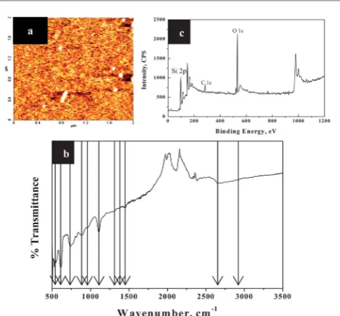
[image:4.595.48.290.473.698.2]The FTIR spectrum of EG functionalized surface presented in Fig. 1b shows a very broad, intense OH valence vibration band near 2600 cm1. All of the OH deformational and skeletal bands are slightly shied to lower wavelength region compared to the
liquid phase EG bands and these shis are consistent with graing of EG-OH onto the silicon substrate via hydrogen bonding. Besides the simple stretching vibrational mode, two additional deformational vibrational modes are readily observed in the spectra at 1420 cm1and 723 cm1. The assignment of the skeletal valance and CH2 deformation vibrations in EG is not facile but comparison to simple molecular hydrocarbon mole-cules can be useful.31Thus, from Fig. 1b, the peaks due to CH
2 deformation are observed are 2942 cm1 (nCH2), 1420 cm1 (dCH2), 1326 cm1 (gCH2), 1268 cm1 (sCH2) and 923 cm1 (rCH2). The peak at 1420 cm1is overlapped with the hydroxyl deformation peak assigned above. The two skeletal valance vibrations in EG can be assigned to peaks at 854 cm1 and 1097 cm1, respectively, of which the lower frequency probably has more C–C character and the other more C–O character. Two other features at 530 cm1and 603 cm1can be assigned O–C–C and O–C–C–O vibrational modes, respectively. All of the features are consistent with EG attachment to the surface. The EG functionalized silicon substrate was further assessed using XPS analysis and data are presented in Fig. 1c. Well-resolved C 1s (284.9 eV), O 1s (533.0 eV) and Si 2p (98.5 eV) features are readily observed (note these values are charge corrected values so the Si 2p peak is observed at 98.5 eV consistent with other studies of silicon wafers). The C 1s feature is consistent with adsorbed features such as adsorbed ethanol.32 The O 1s is similar to that expected of hydroxyl
species in the presence of strong hydrogen bonding.32,33
As detailed above, the silicon substrate with a thin native oxide layer was piranha activated prior to EG deposition. Piranha activation results in the formation of surface OH groups as can be seen from the very low water contact angle (27) on the substrate surface. EG solution in ethanol was spin-coated on the activated surface and exposed in ambient conditions at room temperature (288 K) prior to use. Since the sample was not annealed, it is highly unlikely that condensation reactions between the silanol-OH and EG-OH groups occurred. Instead, it appears that the EG molecules were attached to the substrate surface through hydrogen bonding as suggested by XPS and FTIR. The rather low water contact angle suggests that only one hydroxyl group is used to bond to the surface with the second hydroxyl group available for surface reaction. The availability of one of the OH groups is consistent with the areas of multilayer formation seen in the AFM analysis. It should be noted that the assignment of hydrogen bonding mechanism rather than a condensation reaction of EG-OH groups and surface silanol-OH groups is only partly supported by the XPS, FTIR and contact angle measurements and detailed work may be required. However, we do think this is a valid mechanism as although the EG is strongly bound enough to resist removal during ethanol washes (and subsequent lm deposition), however; all traces of EG are lost upon heating to temperatures above 100C in vacuum.
BCP self-assembly on functionalized surface
By tailoring the surface energy through this simple surface chemistry modication we have developed highly oriented
Fig. 1 AFM topography image (2-D) (a), FTIR spectrum (b) and XPS spectrum (c) of EG functionalized silicon substrate.
stable microdomains with reduced defect densities as evi-denced from the topographic image shown in Fig. 2–5. The periodicity of these domains is 26 nm (cylinder diameter¼20 nm). Thinlms of PS-b-P4VP (24k–9.5k) were generated aer spin coating from a 0.5 wt% BCP solution in toluene–THF mixture (see experimental for further details) onto the EG treated silicon substrate and solvent annealed in a THF atmo-sphere at 50 C. Park et al.34–36 as well as Shin et al.37 have
demonstrated the effectiveness of developing BCP templates from a mixed solvent environment with asymmetric PS-b-P4VP. In some cases even aer spin coating ordered morphologies were obtained, which were improved upon solvent annealing (see ESI, Fig. S1†). In this study, THF which is a slightly PS selective solvent was used for annealing thinlms. The ability of THF to greatly improve lateral ordering has previously been discussed.38
Although most hexagonal forming PS-b-P4VP systems that have been studied are annealed at room temperature (20C) in a nitrogen atmosphere, this produced a combination of mostly poorly ordered perpendicular and parallel cylinders with macroscale dewetting as well as defects in phase sepa-rated areas irrespective of the anneal conditions considered (Fig. 2). Instead a range of temperatures were investigated to yield the most ordered morphology and increasing the temperature provides sufficient driving force for microphase separation to take place forming ordered patterns that is not evident at lower temperatures. Both toluene cleaned and EG treated substrates showed evidence of a both parallel and perpendicular cylinders at different stages of the annealing process. A study of the evolution of morphology of PS-b-P4VP
was examined over 2, 4 and 6 h periods at 40C, 50C and 60C in a THF atmosphere.
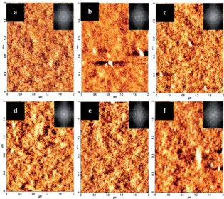
Annealing carried out at 40 C on toluene cleaned substrates is shown in Fig. 3a–c. Well-developed micro-domains were produced aer 2 h annealing, however; surface coverage was poor in comparison to the microdomains produced on EG functionalized substrates at 40C. All AFM images for EG samples taken at 40C show highly ordered domains as represented by the FFT inset in Fig. 3d–f. Samples annealed for 6 h at 50C gave highly uniformlms with high surface coverage and ordered arrays (see Fig. S2†). However, it should be noted that the processing window for these lm characteristics are not limited to one specic time and temperature for EG samples. Furthermore, it was found that thoselms annealed for this time period did not exhibit both perpendicular and parallel cylindrical orientation. Fig. 4c shows the resulting pattern from a PS-b-P4VPlm on toluene only cleaned substrates annealed 50C for 6 h. This compar-ison illustrates the ability that EG has to wet the substrate sufficiently resulting in enhanced surface coverage (see Fig. S2†). Films which were annealed in the same solvent annealing condition but at an elevated temperature of 60C are shown in Fig. 5a–f. With the elevated temperature and longer annealing periods (especially 4 and 6 h) good perpen-dicular domains were developed. With regard to toluene cleaned substrates only, all annealing temperatures showed macroscale dewetting as well as defects. It was generally observed that discrete holes formed in the non-EG treated substrate surface, a phenomenon associated with thin lm destabilisation by intermolecular forces.
Fig. 2 AFM topography images of PS-b-P4VP thinfilms on toluene cleaned bulk silicon substrates ((a) 2 h, (b) 4 h, (c) 6 h) and EG treated substrates ((d)2 h, (e) 4 h, (f) 6 h) annealed in THF atmosphere at 17C (room temperature). FFT patterns inset show the difference in the degree of order.
[image:5.595.67.520.432.701.2]Since hole growth in thinlms is signicantly inuenced by both interfacial and hydrodynamic forces we believe the toluene only cleaned substrates produce more defects and hole growth
due to these intermolecular forces with a bare silicon surface in comparison to substrates that were chemically functionalized with EG.39Also both a mixture of perpendicular and parallel
Fig. 3 AFM topography images of PS-b-P4VP thinfilms on toluene cleaned bulk silicon substrates ((a) 2 h, (b) 4 h, (c) 6 h) and EG treated substrates ((d) 2 h, (e) 4 h, (f) 6 h) annealed in THF atmosphere at 40C. FFT patterns inset show the difference in the degree of order.
Fig. 4 AFM topography images of PS-b-P4VP thinfilms on toluene cleaned bulk silicon substrates ((a) 2 h, (b) 4 h, (c) 6 h) and EG treated substrates ((d) 2 h, (e) 4 h, (f) 6 h) annealed in THF atmosphere at 50C. FFT patterns inset show the difference in the degree of order.
[image:6.595.139.453.49.318.2] [image:6.595.45.533.418.701.2]cylinders has yet to be shown in asymmetric PS-b-P4VP when annealed in a THF atmosphere. Here we employed THF only but THF–toluene (80 : 20) was also studied and produced the same results. This work shows how the patterns are not thermody-namically stable as the structure can change between all perpendicular cylinders and a mixture of both perpendicular and parallel cylinders. We suggest that this mixed orientation results from a swelling/deswelling process as described by Mokarianet al.for PS-b-PEO systems.40Our observation for this
PS-b-P4VP system does not show time or structuraluctuations as dramatic as the PS-b-PEO system mentioned but show similarities that suggest alm thinning effect also occurring and therefore, the release of excess solvent causes a brief rear-rangement of cylinders. So, in summary, we found that 6 h of annealing in a THF atmosphere at 50C gave the most consis-tent pattern that could be utilised for our intended purpose.
The solubility of the BCP blocks is a particular solvent and the rate of solvent evaporation causes the microphase separa-tion as well as orientasepara-tion of the microdomains. Solvent swelling of a BCPlm to a solvent vapour results in swelling the BCPlm with solvent vapours and confers enough mobility for the BCP to reorganize. The miscibility between a polymer and a solvent is governed by the polymer (P)–solvent (S) interaction parametercP–S.41The selectivity of THF for the PS-b-P4VP BCP
can be dened by the expression,c¼Vs(dsdp)2/RT+ 0.34,42 where Vs is the molar volume of the solvent, R is the gas constant,Tis the temperature, anddsanddpare the solubility parameters for solvent and polymer, respectively. From litera-ture,Vsfor THF is 81.7 cm3,dsfor PS, PVP, and THF are 18.6,
22.2, and 16.8 (MPa)1/2, respectively.43Data calculated at various
temperatures are presented in Table 1. Considering the Flory– Huggins criterion for complete solvent–polymer miscibility,i.e.,
cP–S< 0.5, it appears that THF is a good solvent for PS and a poor solvent for PVP at the four temperatures (Table 1). There are minor variations in the values ofcPS–THFandcPVP–THF, both of which slightly decreases with an increase in temperature and infers an decrease in the degree of immiscibility of the polymer with the solvent. It should be noted that the mechanisms of solvent swelling is not well understood. Peng et al.,44 while
studying solvent annealing of PS-b-PMMA in acetone vapour at room temperature observed the vapor molecules attract the PMMA block toward the surface of thelm. The effect of selec-tivity and evaporation rate of solvents on morphology change in PS-b-P4VP lms was studied by Park et al.45 and observed a
morphology change from a dimple type to cylindrical micro-domains oriented perpendicular to surface with increasing THF concentration or as the solvent became less selective for PS. In the present investigation, we believe the substrate interaction of
[image:7.595.138.454.49.328.2]Fig. 5 AFM topography images of PS-b-P4VP thinfilms on toluene cleaned bulk silicon substrates ((a) 2 h, (b) 4 h, (c) 6 h) and EG treated substrates ((d) 2 h, (e) 4 h, (f) 6 h) annealed in THF atmosphere at 60C. FFT patterns inset show the difference in the degree of order.
Table 1 Polymer (P)–solvent (S) interaction parameters (cP–S)
Temperature/C
cP–S
cPS–THF cP4VP–THF
17 0.450 1.328
40 0.442 1.255
50 0.439 1.227
60 0.436 1.201
[image:7.595.302.553.646.731.2]P4VP with ethylene glycol along with the solvent annealing conditions (i.e.solvent and temperature used) thereby draw the PVP block to the surface through the PS-rich layer.
BCPlm reconstruction with ethanol
Surface reconstruction was performed on the solvent annealed sample to facilitate the incorporation of metal nanoparticles. This is possible through the use of a solvent which is non-selective for the majority block, PS in this work, but highly selective for the minor block, P4VP. Samples were immersed for 20 minutes in ethanol and were then dried under nitrogenow. The process leaves the pattern unchanged but yields a useful highly ordered nanoporous lm since P4VP is drawn to the surface as seen in Fig. 6a. Fig. 6b shows a cross-section SEM image (tilt 20) of the surface reconstructedlm revealing well-dened nanopores. The TEM cross-sections in Fig. 6c clearly show that the nanopores are limited to the surface and resides on a thick (20 nm) PS matrix.
Iron oxide(s) hard mask fabrication by inclusion technique
Following surface reconstruction, the spin coating of a low concentration (0.3 wt%) iron nitrate solution in ethanol was carried out toll the nanoporous structure. To prevent over-loading of the pores, a low concentration of metal nitrate solution was employed. Metal deposition from nitrate solutions is a straight forward process as recently outlined in work by Ghoshalet al.46,47However, in the fabrication of a hardmask it is
vital that overloading of the pores is avoided, as it will affect the pattern transfer process aerwards whereby excess iron oxide(s) will be formed on the PS matrix leading to non-uniform etching of the underlying silicon substrate.
Post iron nitrate deposition, UV/Ozone treatment was carried out for a 3 h period which led to the formation of oxide(s) nanodot material and allowed for the removal of the organic polymer matrix. Evidence of FeOxide(s) material is provided in Fig. 7a–c which shows an AFM topography and top-down SEM images of the well-ordered FeOxide(s) nanodots
resembling the template previously represented by PS-b-P4VP BCP. Diameter of these nanodots can be manipulated by altering the initial concentration of the iron nitrate solution. FeOxide(s) nanodots were also examined by calcination in air at 800 C for 1 h to show thermal stability. The top-down SEM image in Fig. 7c shows large area of FeOxide(s) nanodots without any change in periodicity or diameterm.
Analysis of FTIR spectra of various BCPlms aer micro-phase separation provides signicant information about the behaviour of thelm at various stages of FeOxide(s) nanodots fabrication as shown in Fig. 8. The intense peak observed at 1110 cm1 can be assigned to Si–O–Si stretching48 in all the
spectra originating from the native SiO2 layer of the silicon substrate. The stretching of the C–O bonds in PVP which is of interest in the present context can be identied at 970 cm1(ref. 49) for the BCPlms aer microphase separation and ethanol reconstruction. This signature PVP peak is of very low intensity in the iron nitrate loadedlm and could be due to the inter-action of metal ion with the PVP block. UV/Ozone treatment of the iron nitrate loadedlm leads to the complete burn out of the polymer and as such the absence of the PVP peak. It clearly
Fig. 6 Top-down (a) and 20tilted (b) SEM images of surface reconstructed
PS-b-P4VPfilm (see Experimental section for details). Corresponding FFT pattern inset (a) shows the high degree of order. (c) Cross-section TEM image of nano-porous template (inset a low-resolution cross-section TEM image).
Fig. 7 AFM topography image (a), top-down high resolution SEM image (b) of iron oxide nanodots obtained after UV/Ozone treatment for 3 h. (c) The iron oxide nanodot patterns obtained from the UV/Ozone treatedfilm after calcina-tion at 800C for 1 h.
Fig. 8 FTIR spectra of BCPfilms after (a) microphase separation, (b) recon-struction with ethanol for 20 min, (c) iron nitrate loading on the reconstructed film, and (d) UV/Ozone treatment for 3 h.
[image:8.595.311.548.48.245.2] [image:8.595.49.286.514.681.2] [image:8.595.302.555.591.691.2]indicates the existence of metal ion–PVP interaction and does indeed evidence the inclusion of iron nitrate into the porous BCPlm.
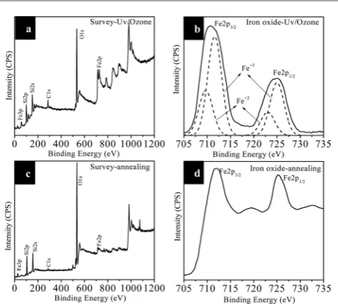
The survey spectra (Fig. 9a and c) of the samples aer UV/Ozone treatment and further annealing/calcination indi-cates presence of the expected elements, Si, O, Fe and a small C 1s (285 eV) feature due to adventitious carbon. High resolu-tion Fe 2p spectra were recorded to distinguish different phases of iron oxides. Fe 2p core level spectrum recorded on iron oxide nanodots prepared aer UV/Ozone treatment (Fig. 9b) consists of two broadened peaks associated with Fe 2p3/2at 710.8 eV and Fe 2p1/2at 724.8 eV due to the existence of both Fe+2and Fe+3 ions. The curvetted Fe 2p3/2and Fe 2p1/2binding energies are 709.6 and 722.8 eV (assigned to Fe+2) and 711.5 and 724.9 eV (assigned to Fe+3), respectively, matches literature values.50The
concentration ratio of Fe+3/Fe+2was calculated from the curve-tted peak areas as about 2 : 1 as expected for Fe3O4. Fe 2p core level spectrum of iron oxide nanodots aer annealing/calcina-tion (Fig. 9d) consists of two sharp peaks at 711.5 and 725.1 eV associated with Fe 2p3/2 and Fe 2p1/2 accompanied by high binding energy satellite structures (+8 eV shi). These data are consistent with the existence of Fe+3(Fe
2O3) ions only.51,52Thus, XPS analysis conrms the formation of phase pure iron oxides without any polymer residues.
GISAXS of BCPlms at different stages
Further evidence of lm morphology is provided by grazing incident small angle X-ray scattering (GISAXS) data gathered as shown in Fig. 10a–c. The data obtained was measured above the critical angle of the polymer but below the critical angle for silicon. With this incidence angle (a¼0.20) the reected X-rays from the silicon interface enhance the scattering observed from the PS-b-P4VPlms, specically for the reconstructed and iron nitrate containing lms owing to the large electron density
difference. No diffraction features were observed for the initially microphase separated PS-b-P4VP structure on silicon oxide surface functionalized with an ethylene glycol layer (Fig. 10a) most likely due to the low electron density between the two polymer blocks. However, following surface reconstructionrst order diffraction spots were observed (Fig. 10b). Furthermore, aer loading of the reconstructedlms with iron nitrate the intensity of the diffraction spots increased (Fig. 10c), indicating that the metal ions arelling the void spaces in thelm. As seen from Fig. 10b and c the scattering alongQzindicates that the cylindrical microdomains are oriented perpendicular to the surface. Interestingly, the diffraction spots seen in Fig. 10b are not as intense as one would expect most likely due to the fact that the pores do not traverse the entire lm, as discussed earlier from TEM data (Fig. 6c). It should also be noted that the specular beam spot in Fig. 10b has become more diffuse sug-gesting that the reconstructedlm has become rougher.
It was also noticed that thed-spacings of these diffraction spots in the reconstructed and metal loadedlms was not the same with the periodicity increasing from 24.6 nm to 29.7 nm. This is somewhat unexpected as the PS block is not solvated at all by the aqueous solution from which the metal ions are cast and therefore were not expected to be affected by the metal loading. In increasing the periodicity of thelms the loading of the metal ions is causing a distortion of the PS matrix of the lm, which presumably is accommodated by a stretching of the PS polymer chains. This distortion of the polymer matrix cannot however be simply accommodated across thelm as a whole and we would therefore expect the formation of fault lines and defects in the lm as a direct result of this expansion. X-ray reectometry experiments were also attempted, but these did not yield any meaningful results.
[image:9.595.47.289.473.690.2]Fabrication of silicon nanopillars
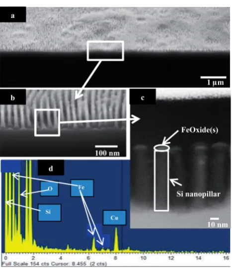
Fig. 11a–c shows the silicon nanopillars fabricated following pattern transfer using the FeOxide(s) nanodot array template. SEM images in Fig. 11a and b conrm high surface coverage resulting and conrms that the FeOxide(s) template provided an ideal etch mask to develop these high aspect ratio silicon nanopillars. Additionally the high degree of order seen with the BCP thin lm template is represented in the nanopillars structures in Fig. 11b. This SEM image shows a high degree of order with silicon nanopillars diameter averaging 16 nm. Nanopillar structure height varies between 115 and 120 nm giving an aspect ratio of 1 : 6. This small difference in nano-pillar height shows that the silicon etch used works satisfacto-rily even though the etch was performed for only 12 s. Again this point extends the signicance of employing a metal oxide etch mask whereby high delity silicon nanostructures can be obtained in a relatively short period and by using a simple bottom up methodology. Further evidence of FeOxide(s) deposited on the silicon substrate is shown in Fig. 11c. The high-resolution SEM image clearly shows the presence of FeOxide(s) nanodot on the top of the silicon nanopillar.
To verify the presence of Fe in the nanodots fabricated, EDX was performed in point mode to locate Fe on top of the
Fig. 9 XPS survey (a and c) and high resolution Fe 2p core level (b and d) spectra of iron oxide nanodots on silicon substrates after UV/Ozone treatment (a and b) and calcination/annealing (c and d).
nanopillar. It should be noted that when EDX is being carried out, it results in the deposition of a large amount of carbon on the sample, and since the feature of interest is small (20 nm of FeOxide(s) on Si nanopillars) this then results in the rapid build-up of carbon on the sample surface which obscures the X-ray signals. For this particular reason, EDX is performed on a single point on the sample rather than obtaining a map of the elemental composition. From the EDX spectrum in Fig. 11d, peaks are visible identifying that Fe is indeed present at the top
of the silicon nanopillar structure. However these peaks are extremely small, representative of the low quantity of metal deposited on the silicon substrate, which accounts for the major peak. It should be noted that the intense copper peak seen in the spectrum is due to the grid used during analysis.
Conclusions
In conclusion, we have demonstrated a facile method for the enhancement of surface coverage and ordering through a molecular functionalization based around ethylene glycol which favourably interacted with PS-b-P4VP forming an ideal perpendicularly orientated template. This orientation along with surface reconstruction process allowed for the successful incorporation of a FeOxide(s) hard mask which enabled the fabrication of high aspect ratio silicon nanopillars. Addition-ally, further information was provided in this report with GISAXS and spectroscopic data aiding the understanding on lm morphology following the reconstruction and iron nitrate deposition process. In summary, we have shown a simple approach using block copolymer lithography for the fabrication of silicon nanopillars with high degree of order anddelity.
Acknowledgements
We thank Diamond Light Source for access to beamline I07 (SI 8065) that contributed to the results presented here. Financial support for this work is provided by the EU FP7 NMP project, LAMAND (grant number 245565) project and the Science Foundation Ireland (grant number 09/IN.1/602), and gratefully acknowledged. The support of SFI through the CRANN CSET is also appreciated.
References
1 R. A. Segalman,Mater. Sci. Eng., R, 2005,48, 191.
[image:10.595.137.457.49.230.2]2 C. Park, J. Yoon and E. L. Thomas,Polymer, 2003,44, 6725. 3 Y.-C. Tseng and S. B. Darling,Polymer, 2010,2, 470.
Fig. 10 GISAXS patterns of the BCPfilm after (a) microphase separation, (b) reconstruction with ethanol for 20 min, and (c) iron nitrate loading on the reconstructedfilm.
Fig. 11 Fabrication of silicon nanopillars following pattern transfer process using FeOxide(s) as etch mask. Cross-section low-resolution SEM (a), high-resolution SEM images (70tilted) (b and c) of silicon nanopillars. (d) EDX spectrum of (a).
[image:10.595.51.285.281.551.2]4 R. A. Farrell, N. Petkov, M. A. Morris and J. D. Holmes,J. Colloid Interface Sci., 2010,349, 449.
5 I. W. Hamley,Nanotechnology, 2003,14, R39.
6 J. K. Kim, S. Y. Yang, Y. Lee and Y. Kim,Prog. Polym. Sci., 2010,35, 1325.
7 T. P. Lodge,Macromol. Chem. Phys., 2003,204, 265. 8 C. T. Black,ACS Nano, 2007,1, 147.
9 H. Cho, S. Choi, J. Y. Kim and S. Park,Nanoscale, 2011,3, 5007.
10 J. Xu, T. P. Russell, B. M. Ocko and A. Checco,SoMatter, 2011,7, 3915.
11 J. N. L. Albert and T. H. Epps III, Mater. Today, 2010,
13, 24.
12 D. Y. Ryu, J.-Y. Wang, K. A. Lavery, E. Drockenmuller, S. K. Satija, C. J. Hawker and T. P. Russell,Macromolecules, 2007,40, 4296.
13 J. Bang, J. Bae, P. Lowenhielm, C. Spiessberger, S. A. Given-Beck, T. P. Russell and C. J. Hawker,Adv. Mater., 2007,19, 4552.
14 D. Y. Ryu, S. Ham, E. Kim, U. Jeong, C. J. Hawker and T. P. Russell,Macromolecules, 2009,42, 4902.
15 S. H. Kim, M. J. Misner and T. P. Russell,Adv. Mater., 2008,
20, 4851.
16 W.-H. Huang, P.-Y. Chen and S.-H. Tung, Macromolecules, 2012,45, 1562.
17 S.-H. Tung and T. Xu,Macromolecules, 2009,42, 5761. 18 W. van Zoelen, E. Polushkin and G. ten Brinke,
Macromolecules, 2008,41, 8807.
19 R. Maki-Ontto, K. de Moel, W. de Odorico, J. Ruokolainen, M. Stamm, G. ten Brinke and O. Ikkala,Adv. Mater., 2001,
13, 117.
20 B. K. Kuila, E. B. Gowd and M. Stamm,Macromolecules, 2010,
43, 7713.
21 D. Borah, M. T. Shaw, S. Rasappa, R. A. Farrell, C. O. Mahony, C. M. Faulkner, M. Bosea, P. Gleeson, J. D. Holmes and M. A. Morris,J. Phys. D: Appl. Phys., 2011,
44, 174012.
22 D. Borah, S. Rasappa, R. Senthamaraikannan, M. T. Shaw, J. D. Holmes and M. A. Morris, J. Colloid Interface Sci., 2013,13(393), 192.
23 E. B. Gowd, B. Nandan, M. K. Vyas, N. C. Bigall,
A. Eychmueller, H. Schloerb and M. Stamm,
Nanotechnology, 2009,20, 415302.
24 H. Yoo and S. Park,Nanotechnology, 2010,21, 245304. 25 T. Xu, J. Stevens, J. A. Villa, J. T. Goldbach, K. W. Guarim,
C. T. Black, C. J. Hawker and T. R. Russell, Adv. Funct. Mater., 2003,13, 698.
26 J. Q. Lu,J. Phys. Chem. C, 2008,112, 10344.
27 Y. Liu, C. Lor, Q. Fu, D. Pan, L. Ding, J. Liu and J. Lu,J. Phys. Chem. C, 2010,114, 5767.
28 L. X. Song, Y. M. Lam, C. Boothroyd and P. W. Teo,
Nanotechnology, 2007,18, 13.
29 H.-Y. Si, J.-S. Chen and G.-M. Chow,Colloids Surf., A, 2011,
373, 82.
30 C. T. Black, R. Ruiz, G. Breyta, J. Y. Cheng, M. E. Colburn, K. W. Guarini, H. C. Kim and Y. Zhang, IBM J. Res. Dev., 2007,51, 605.
31 J. H. Schachtschneider and R. G. Snyder,Spectrochim. Acta, 1963,19, 117.
32 A. F. Lee, D. E. Gawthrope, N. J. Hart and K. Wilson,Surf. Sci., 2004,548, 200.
33 V. M. Bermudez, A. D. Berry, H. Kim and A. Piqu´e,Langmuir, 2006,22, 11113.
34 S. Park, J.-Y. Wang, B. Kim, J. Xu and T. P. Russell,ACS Nano, 2008,2, 766.
35 S. Park, B. Kim, J.-Y. Wang and T. P. Russell, Adv. Mater., 2008,20, 681.
36 S. Park, J.-Y. Wang, B. Kim and T. P. Russell,Nano Lett., 2008,
8, 1667.
37 D. O. Shin, D. H. Lee, H. S. Moon, S. J. Jeong, J. Y. Kim, J. H. Mun, H. Cho, S. Park and S. O. Kim, Adv. Funct. Mater., 2011,21, 250.
38 S. Park, B. Kim, J. Xu, T. Hofmann, B. M. Ocko and T. P. Russell,Macromolecules, 2009,42, 1278.
39 R. Limary and P. F. Green,Langmuir, 1999,15, 5617. 40 P. Mokarian-Tabari, T. W. Collins, J. D. Holmes and
M. A. Morris,ACS Nano, 2011,5, 4617.
41 J. Brandrup, E. H. Immergut, E. A. Grulke and A. Abe,D. R. Bloch in Polymer Handbook, John Wiley & Sons, New York, 4th edn, 1999.
42 J. E. Mark, inPhysical Properties of Polymers Handbook, AIP Press, New York, 1996.
43 D. W. van Krevelen,Properties of Polymers, Elsevier Scientic Publishing Company, Amsterdam, Oxford, New York, 1976. 44 J. Peng, D. H. Kim, W. Knoll, Y. Xuan, B. Li and Y. Han,J.
Chem. Phys., 2006, 125.
45 S. Park, J.-Y. Wang, B. Kim, W. Chen and T. P. Russell,
Macromolecules, 2007,40, 9059.
46 T. Ghoshal, M. T. Shaw, C. T. Bolger, J. D. Holmes and M. A. Morris,J. Mater. Chem., 2012,22, 12083.
47 T. Ghoshal, T. Maity, J. F. Godsell, S. Roy and M. A. Morris,
Adv. Mater., 2012,24, 2390.
48 D. Borah, S. Rasappa, R. Senthamaraikannan, B. Kosmala, M. T. Shaw, J. D. Holmes and M. A. Morris, ACS Appl. Mater. Interfaces, 2012,5, 88.
49 S. Magazu, F. Migliardo and A. J. Ramirez-Cuesta,J. R. Soc., Interface, 2007,4, 167.
50 R. Prakash, R. J. Choudhary, L. S. S. Chandra, N. Lakshmi and D. M. Phase,J. Phys.: Condens. Matter, 2007,19, 486212. 51 P. Mills and J. L. Sullivan,J. Phys. D: Appl. Phys., 1983,16,
723.
52 T. Fujii, F. M. F. de Groot, G. A. Sawatzky, F. C. Voogt, T. Hibma and K. Okada, Phys. Rev. B: Condens. Matter Mater. Phys., 1999,59, 3195.