Centre for Electr onics Design and Technology of India
An Autonomous Scientific Society under Department of Electronics, Govt. of India,
New Delhi.
First Edition: 1999
TRADEMARKS: All brand name and product names mentioned in this book are trademarks or registered trademark of their respective companies.
Ever y effort has been made to supply complete and accurate information. However, CEDTI assumes no responsibility for its use, nor for any infringement of the intellectual property rights of third par ties which would result from such use.
No part of this publication may be stored in a retrieval system, transmitted or reproduced in any for ms or by any means, electronic, photocopy, photograph, magnetic or otherwise, without written permission of CEDTI.
The information technology and telecom sectors have suddenly opened up avenues, which require a very large specially trained manpower. These sectors are highly dynamic and need training and re-training of manpower at a rapid rate. The growing gap of requirement of the industry and its fulfillment has created a challenging situation before manpower training institutes of the country. To meet this challenge most effectively, Centre for Electronics Design and Technology of India (CEDTI) has launched its nation-wide franchising scheme.
Centre for Electronics Design and Technology of India (CEDTI) is an Autonomous Scientific Society under the Govt. of India, Department of Electronics with its Headquarters at New Delhi. It operates seven centres located at Aurangabad, Calicut, Gorakhpur, Imphal, Mohali, Jammu and Tezpur. The scheme will be implemented and coordinated by these centres.
The scheme endeavours to promote high quality computer and information technology education in the country at an affordable cost while ensuring uniform standards in order to build a national resource of trained manpower. Low course fees will make this education available to people in relatively small, semi urban and rural areas. State-of-the-art training will be provided keeping in view the existing and emerging needs of the industrial and Govt. sectors. The examinations will be conducted by CEDTI and certificates will also be awarded by CEDTI. The scheme will be operated through all the seven centres of CEDTI.
The CEDTI functions under the overall control and guidance of the Governing Council with Secretary, Department of Electronics as its Chairman. The members of the council are drawn from scientific, government and industrial sectors. The Centres have separate executive committees headed by Director General, CEDTI. The members of these committees are from academic/professional institutes, state governments, industry and department of electronics.
CEDTI is a quality conscious organisation and has taken steps to formally get recognition of the quality and standards in various activities. CEDTI, Mohali was granted the prestigious ISO 9002 certificate in 1997. The other centres have taken steps to obtain the certification as early as possible. This quality consciousness will assist CEDTI in globalizing some of its activities. In keeping with its philosophy of ‘Quality in every Activity’, CEDTI will endeavour to impart state of the art – computer and IT training through its franchising scheme.
Maintenance Course levels is to train the students to diagnose the faults and carry out repairs at card level in computers, instruments, EPABX, Fax etc. and other office equipment. At Engineer and Network Engineer levels the thrust is to train them as System Engineers to install and supervise the Window NT, Netware and Unix Networking Systems and repair Microcontrollers / Microprocessor based electronic applications.
An Advisory Committee comprising eminent and expert personalities from the Information Technology field have been constituted to advise CEDTI on introduction of new courses and revising the syllabus of existing courses to meet the changing IT needs of the trade, industry and service sectors. The ultimate objective is to provide industry-specific quality education in modular form to supplement the formal education.
The study material has been prepared by the CEDTI, document centre. It is based on the vast and rich instructional experience of all the CEDTI centres. Any suggestions on the improvement of the study material will be most welcome.
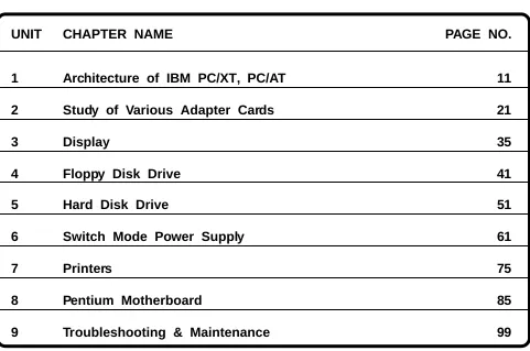
TABLE OF CONTENTS
UNIT CHAPTER NAME PAGE NO.
1 Architecture of IBM PC/XT, PC/AT 11
2 Study of Various Adapter Cards 21
3 Display 35
4 Floppy Disk Drive 41
5 Hard Disk Drive 51
6 Switch Mode Power Supply 61
7 Printers 75
8 Pentium Motherboard 85
This volume of course material has been designed as an introductory course in PC Architecture and Troubleshooting as a part of the T-Level course under CFS. The aim is to enable a student, executive or a working professional to effectively assemble, install and upgrade a computer and know various sub-assemblies involved in the process.
Our approach is to stress the fundamental concepts of IBM PC, IBM PC-XT, PC-AT. By this approach with a diversity of application. We hope to convey both the substance and flavour of the subject. The breadth and depth of treatment also make this volume a valuable adjunct to continuing education of Practicing technicians and engineers.
This book has substantial amount of new material that has been added to reflect changes in technology and curricula. This book helps you by way of offering useful and practical tips suggestions.
The chapter one deals with Architecture of IBM PC, PC/XT and PC/AT. It covers the basic hardware components required by the personal computers. Chapter two deals with various peripheral adapter cards such as FDC, IDE, CGA and GIST cards. Chapter four deals with Floppy Disk Drives, Chapter Five, Six and Seven focusses on the SMPS, hard Disk Drives and Printers. Chapter Eight deals with Pentium Motherboards. Chapter Nine focuses on troubleshooting techniques used in repairing and maintenance of PCs.
ARCHITECTURE OF IBM PC/XT, PC/AT
COMPETENCY OBJECTIVES
The objective of this Chapter is to make students understand the basic architecture of PC/ XT Motherboard and PC/AT Motherboard. At the end of this section, a student should be able to
:-v Logically differentiate between XT and AT motherboards.
v Visualize the differences between the two motherboards.
CHAPTER - 1
ARCHITECTURE OF IBM PC/XT, PC/AT
1.0 INTRODUCTION TO ARCHITECTURE OF IBM PC/XT
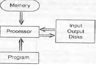
[image:9.612.221.410.341.477.2]PC/XT is Personnel Computer with Extended technology. There are five key parts of a computer. These are Processor (sometimes called as Central Processing Unit) the input/output circuitry, disk storage and Program. There are also other components that form parts of packaging and support such as power supply, the motherboard, the bus and peripherals.
Figure 1.1 Components of a PC
The usual Components on the motherboard are the main Processor chip & its support chips; memory and I/O interface (Serial Port, Parallel Port, Keyboard interface, disk interface, and so on).
The PC/XT may have following specifications,
CPU (Processor) 8088 - 2 Or V - 20
Data (Bus) 16-Bits
Crystal Frequency 4.77 to 13 MHz. Memory (Primary) 640 KB
Floppy Disks (FD) 360 KB
1.1 MEMORY SPACE
The 8088 has a 20-bit address bus. Hence it can address upto 1 Megabyte of memory. Since each location is one byte, theoretically the PC can have upto 1-megabit program. 1MB memory space includes both Random Access Memory (RAM) and Read only Memory (ROM).
1.1.1 CPU
The PC/XT has Intel 8088 processor, which has a 16-bit internal data bus while but an 8-bit external data bus. The 16-bit internal bus provides high speed Processing Power. The 8-bit data bus provides an easy interfacing capability and compatibility with 8-bit systems. In PC/ XT there is provision for the 8087 a floating-point processor to work as a co-processor with 8088 CPU.
The program memory is split into RAM and ROM. The ROM contains Permanent programs. The RAM is used to store application programs and also system programs.
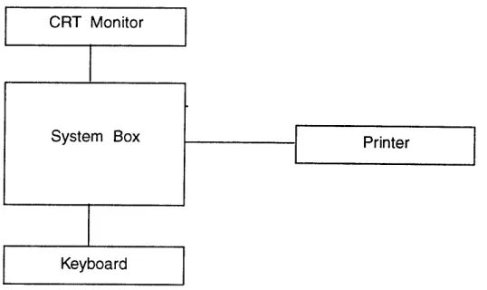
[image:10.612.165.434.336.496.2]1.1.2 PC HARDWARE
Fig. 1.2 Block Diagram of the system
The blocks shown in figure are the system unit, which houses CPU, Memory, DMA, and Peripheral controllers . The external units, which are outside the system box, are keyboard, CRT Monitor, Printer, Modem etc. Additional memory, Peripheral Controllers can also be used in case the application software needs.
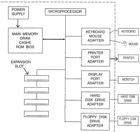
1.2 HARDWARE COMPONENTS OF A COMPUTER SYSTEM
PC System has eight major hardware elements
1) Central Processing Unit (CPU) : In most PCs today that is Intel 486 or Pentium or any Intel Compatible Processor are used.
2) IO Devices : Input devices are Keyboard, mouse, Scanner, CD ROM drives etc. While the common output devices are printers and displays monitors.
3) Memory : A set of high speed memory and slower storage devices to save and retrieve programs and data.
4) BUS : A set of connect the microprocessor to its memory and to the adapters that enable connections to other devices through their output ports or expansion slots.
5) Adapters : A set of control cards that enables the microprocessor to communicate with and control I/O devices or storage devices. These adapters that are set of hardware circuitry that attach to the system bus and convert each bus to an interface port supporting the attachment of specific I/O ports.
6) Ports : Ports are hardware interfaces created by the adapters supporting the attachments of I/O devices.
7) Expansion slots : Permits easy expansion or upgrading of PC system with new I/O devices and or memory.
ARCHITECTURE OF IBM PC/XT, PC/AT
Fig. 1.3 : A Simplified Block Diagram of a PC System
1.3 ARCHITECTURE OF IBM PC-AT
IBM PC/AT VERSIONS
There are two versions of IBM PC/AT
1. A Base Model 2. An Enhanced Model
The base model does not have a hard disk whereas enhanced model has a hard disk. The original base model has a 256KB RAM on the motherboard and enhanced model has a 512KB RAM on motherboard. Both the models can support 360KB FDD and 1.2MB FDD.
Each memory bank is 128 KB. The new version IBM PC/AT uses 256 KB DRAM.
The keyboard used in initial version has 84 keys including 10 function keys. While new version support 101 key enhanced keyboard with 12 function keys. The enhanced version AT has a Serial /Parallel adapter.
1.3.1 Hardware Overview of IBM PC-AT
The IBM PC-AT provides compatibility to PC daughter board by providing similar bus on I/O slots and additional signals to support more data and address bits.
In IBM PC ROM, RAM on motherboard are placed on separate and isolated internal
1.3.2. PC-AT-286 HARDWARE OVERVIEW
The PC-AT-286 uses an Intel 80286 Microprocessor. The Co-processor used by IBM is 80287. The PC-AT-286 uses two clock generator chips an 82284 & 82284. The 8284 is used to generate 14.318 MHz clock signal. The purpose of this signal is to provide compatibility for CGA board. The 82286 is used to generate clock signals to 80285 & 80857. The 80285 divides input clock frequency by two. The input clock frequency can be typically 12 MHz, 16 MHz, or 20 MHz. The clock generator also generates RESET, READY signal to 80286. The 82288 bus controller is used for generating bus control signals which identify the type of bus i.e. for 80286.
The PC-AT uses two 8237A DMA Controllers for providing eight DMA Channels. The DMA Channels 0,1,2,3 are used for date transfer involving 8-bit I/O, adapters & 8 or 16-bit system memory. The channels 5,6,7 are used for 16 bit data transfer involving 16-bit I/O adapters and 16 bit system memory.
Two 8259A chips are cascaded to provide 15 interrupt level in the PC-AT.
PC-AT uses 8254-2 timer/counter chip, which has three programmable time/counters. The use of three counters is as shown in below.
TIMER CHANNEL FUNCTION
0 IRQo-System timer
1 Memory Refresh Request
2 Speaker Tone Generator
The ROM chips used are byte organized. But the width of the system data is 2 bytes (16-bits). Hence Two ROM chips are used. One to store odd location & other to store even locations.
The keyboard interface is provided by a single chip microcomputer such as 8042 & 8742.
1.3.3. Display Switch
This is only DIPSwitch used in PC-AT it indicates whether an MDA or CGA board is installed in PC-AT. If the switch is set wrongly the post senses the error, and indicates this to the user by the error beeps.
1.3.4. Jumper Options
In PC-AT jumper options are provided to select the system configuration such as speed, number of wait states, selection of parallel ports, selection of serial ports, RAM banks, etc.
1.3.5. Memory Refresh in AT
counter gives LSB address bits. Along with this counter, DMA page register in used to generate MSB address bits.
ASSIMILATION EXERCISE
Q.1 What are Hardware Components of a system? Q.2 What is data width of 8088?
Q.3 What is the difference between PC/XT & PC/AT? Q.4 How many expansion slots are there in PC & PC-XT? Q.5 List the input and output devices of PC?
Q.6 How many pins are there on Power Connector on PC-AT motherboard? Q.7 What is the necessity of 8087 in PC-XT?
Q.8 Which Peripheral devices use +12V Supply output of SMPS? Q.9 How many IRQ’s are uses in PC-XT?
STUDY OF VARIOUS ADAPTER CARDS
COMPETENCY OBJECTIVES
The objective of this Chapter is to make students understand the the types of various add-on cards. At the end of this sectiadd-on, a student should be able to
:-v Logically differentiate between various display adapter cards.
v Visualize various signals available in a Floppy drive controller card.
v Understand various Hard disk controllers.
v Understand external Modem to PC Connection.
CHAPTER - 2
STUDY OF VARIOUS ADAPTER CARDS
2.0 VARIOUS DISPLAY ADAPTER CARDS AND THEIR IDENTIFICATION
The PC is connected to the monitor through display adapter cards. The present PC display adapter card is mounted on motherboard expansion slots.
There are number of display adapter cards, the list of them is as below :
1) MDA - Monochrome Display Adapter 2) CGA - Color Graphics Adapter 3) HGA - Hercules Graphics Adapter 4) EGA - Enhanced Graphics Adapter 5) VGA - Video Graphics Adapter
6) SVGA - Super Video Graphics Adapter 7) XGA - Extended Graphics Adapter
These cards can be identified by the following points.
Sr.No Card Type Connector Pins Video Memory Edge Connector Additional Connector
1. MDA D Shell
9 Pin
4 KB 16 PIN Nil
2. CGA D Shell
9 Pin
16 KB 32 PIN Printer Connector
3. EGA 9 Pin
D Shell
64KB-256KB 32 PIN Printer Connector
4. VGA 15 Pin
Female
256KB-1 MB 16 PIN NIL
2.0.1 The signals of display adapter cards
On the Pin Connector
MDA 9 PIN CONNECTOR
PIN NOS. SIGNAL (MDA)
1 Ground
2 Ground
3, 4, 5 Not used 6 Intensity
7 Video
8 Hsync
9 Vsync
CGA 9 PIN CONNECTOR
PIN NOS. SIGNAL (MDA)
1 Signal 2 Ground 3 Ground 4 Red 5 Blue 6 Intensity 7 Reserved 8 Hsync 9 Vsync
EGA 9 PIN FEMALE CONNECTOR PIN NOS. SIGNAL (MDA)
1 Signal
2 Ground
3 Secondary Red 4 Primary Red 5 Primary Green 6 Primary Blue
7 Secondary Green / Intensity 8 Secondary Blue/Mono Intensity
STUDY OF VARIOUS CARDS
2.2 FDC CARD
Floppy Disk Control board is linked to the system bus of the PC. It appears as a set of I/O parts to the CPU. A single FDC can support upto 4 Floppy Disk Drives. The FDC communicates with the CPU and the FDD.
The FDD has two connectors
1. Signal connector P1/J1 2. DC Power connector P2/J2
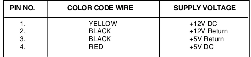
Table gives voltages on different pins of this connector.
PIN NO. COLOR CODE WIRE SUPPLY VOLTAGE
1. YELLOW +12V DC
2. BLACK +12V Return
3. BLACK +5V Return
4. RED +5V DC
All the device signals are low active. A 34 pin flat cable is used and odd numbered wires are grounded.
GND Pin Signal Pin Signal Name Function
1 2 ---
---3 4 ---
---5 6 ---
---7 8 INDEX Indicates start of track
9 10 MOTOR ENABLE 0 Turns on drive 11 12 DRIVE SELECT1 Selects drive 1 13 14 DRIVE SELECT 0 Select drive 0
15 16 MOTOR ENABLE1 Turns on drive spindle 1
17 18 DIRECTION When active, the R/W head moves inward. When inactive head moves outward.
19 20 STEP When low, the R/W head moves by one track in the direction decided by DIRECTION signal
21 22 WRITE DATA MFM writes data to the FDD Enables writing of data.
23 24 WRITE ENABLE Enables writing of data
25 26 TRACK0 Indicates R/W head is over the outmost track.
27 28 WRITE PROTECT Indicates that write protected diskette is present in FDD.
29 30 READ DATA MFM Read data from FDD. 31 32 HEAD SELECT 1 When high selects head 0,
When low indicates head 1.
---2.3 HARD DISK CONTROLLER CARD
Hard disk is magnetically coated disks. The disks are rigid platters of an aluminum alloy. The hard disk controller is connected to hard disk card itself. The hard disk drive and hard disk controller have a plug in connector on the connectors of the edges of the Printed Circuit Boards.
The controller and data cable should then be connected to the controller. The connector often used for this purpose can often be connected incorrectly so be careful when attaching the cable. The various control signals are listed below.
GND Pin Signal Pin Signal Name Description
1 2 REDUCE WRITE
CURRENT HEAD SELECT3
Some controllers use thi spin as RWC , to reduce write current on inner cylinder.
3 4 HEAD SELECT 2 One of three head select signals
5 6 WRITE GATE Issued when data is to be
written on HDD
7 8 SEEK COMPLETE Indicates that head has reached the desired cylinder and has stabilised.
9 10 TRACK 000 Indicates that heads are
positioned over the cylinder 0. 11 12 WRITE FAULT Indicates a write error.
13 14 HEAD SELECT0 One of the three head select signals.
15 -
-16 -
-17 18 HEAD SELECT One of the three head select signals.
19 20 INDEX PULSE Indicates the beginning of a track
21 22 DRIVE READY Indicates motor is upto speed. 23 24 STEP PULSE For each step pulse, head
moves by one track.
25 26 DRIVE SELECT 0 The controller issues this signals when drive 0 has to be selected. 27 28 DRIVE SELECT 1 The controller issues this signal when drive 1 has to be selected.
29 30 DRIVE SELECT 2 Not used
31 32 DRIVE SELECT 3 Not used
POWER CONNECTOR
The power supply requires is +5v and +12v . DC power connector pin assignments.
PIN NOS. COLOR CODE WIRE SUPPLY VOLTAGE
1 YELLOW +12 V DC
2 BLACK 12 V DC
3 BLACK - 5 V DC
4 RED +5 V DC
Data cable connection to be added
2.4 IDE CARD
The IDE is intelligent drive electronics also known as ATA port. This card supports attachment of two hard drives with maximum capacity of 528 MB each. When PC/AT was announced by IBM, the hard disk drive adapter was a separate adapter board installed in an PC/AT.
The interface cable from drive is attach to a 40 pin header organised as two rows of 20 pins with 20 functioning keys. Two drives are connected by a single cable connected in a daisy chain system.
PIN DESCRIPTION PIN DESCRIPTION
1 Host 21 DMA Request
2 Not used 22 GND
3 Data bus bit 7 23 I/O Write
4 Data bus bit 8 24 GND
5 Data bus bit 6 25 I/O Read
6 Data bus bit 9 26 GND
7 Data bus bit 5 27 I/O Ready
8 Data bus bit 10 28 Spindle Syne
9 Data bus bit 4 29 DMA acknowledge
10 Data bus bit 11 30 GND
11 Data bus bit 3 31 Interrupt Request 12 Data bus bit 12 32 16 bit I/O
13 Data bus bit 2 33 Device address bit 1 14 Data bus bit 13 34 Passed Diagnostic 15 Data bus bit 1 35 Device address bit 0 16 Data bus bit 14 36 Device address bit 2 17 Data bus bit 0 37 Chip select 0
18 Data bus bit 15 38 Chip select 2
19 Ground 39 Device active
IDE Card has cable header of Floppy disk & Hard disk drive.
2.5 MULTI I/O PORT ADAPTER BOARD
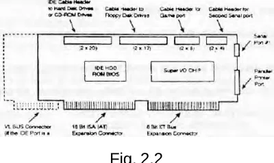
[image:25.612.215.415.160.279.2]This board supports a number of peripheral interface adapter and ports fig 2.2 is as shown below.
Fig. 2.2
The Board permits to attach IDE (hard disk controller port) typically all the device adapter and ports on the multi I/O port board are integrated on a single chip called super I/O. The board has.
1. Hard Disk Drive cable header. 2. Cable header for FDD
3. Cable header for Game port.
4. Cable header for second Game port. 5. Serial port connector.
6. Parallel printer port.
2.6 STUDY OF SVGA CARD
SVGA is Super Video Graphics Adapter Card. Most of the available boards today are Super VGA cards.
It supports
Text 128x48
Character size 8x16 Graphics 1024x768
Display Mode 1280x1024 pixel raster with 24 bit /pixel
2.7 MODEMS AND THE PC CONNECTION
PCs can attach to modem in three primary ways :
1. External device connected to the PC with a cable attached to one of the PC’s serial communications parts.
2. As an internal device that plugs into one of the PC’s expansion slot.
3. As a PCMCIA card that plugs into PC’s PCMCIA slot(usually on notebook).
External Modem PC Connection as shown in Fig. 2.3 below:
The external Fax/Modem attached to one of the PC’s serial communication ports on the PC, the serial communication ports are often referred as com1 , com2, com3, com4. Most PC’s today have com1, com2 as Multi I/O ports. On the PC, the COM ports are created by chips called UART, which interfaces two PC IAS buses, and take bytes of data and convert them to a serial bit stream.
Each byte of the data is framed in a start bit and followed by a parity check bit and 1,1½ or 2 stop bits. The UART generates a set of control signals and senses input signals and from the modem signals that are used to unsure that a connection with external modem is in placed. Both the serial ports send and receive data streams and modem control and status leads are then converted electrically to special voltage level.
Advantage of External Modems
1. Can be used on any system that has a serial port and not limited to just PCs. 2. Protection to telephone lines from power surge.
communication could not support faster data transmission. Newer UART 16550 overcomes all these shortcomings.
Internal modem is an ADD ON CARD, which has on board 16550 UART thereby it supports the higher data rate.
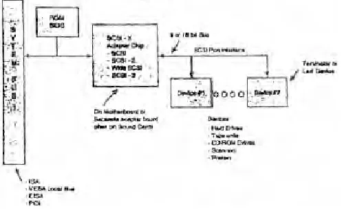
2.8 SCSI CARD
[image:27.612.192.442.380.535.2]SCSI is Small Computer System Interface. The SCSI specification first served the needs of the hard disk industry. The SCSI interface is an intelligent and high performance I/O interface. It is a common interface incorporated in disk drives, printers and type drives. The SCSI specification defines a logical command set for each generic peripheral type. Any device can communicate directly with any other device over SCSI bus. The specification defines bus phases that allow for bus arbitration and temporary disconnection. The SCSI specification device can queue multiple commands in the local controller and execute them in correct order. Therefore SCSI I/O is used for multi-user multitasking system application. This SCSI bus also serves as cost effective because it supports variety of peripherals such as hard disk drives and CD-ROM drives and high speed tape backup drives. SCSI is a host independent interface, it is also possible to move SCSI device from say on Apple MAC system to a PC system. SCSI software device driver must be installed on to PC to support the SCSI port and devices. The manufacturer provides this driver.
Fig. 2.4
2.9 GIST INTRODUCTION
GIST is hardware and software product.
GIST provides a special SCRIPT PAGE, which is used by custom packages like the script processor for allowing versatile word processing in multiple scripts. Script page provides various attributes like bold, outline, etc., which can arbitrarily mixed along with multiple script. Scripts page even allows proper mixing of scripts which flow in different direction such as is required when English words are to be display within Urdu text. DATA PAGE looks identical to IBM screen, while allowing display of complex scripts within the same 80 characters by 25-row format. Although the non-English scripts are proportionally spaced they still remain aligned properly in columnar text display. In addition data page provide 7-bit mode which allows use of environment that only 7-bit data.
GIST uses standard (ISCII) Indian Standard Code for Information Interchange and inscript keyboard to chatter to all the Indian scripts in uniform way. This also is the basis of instantaneous transliteration facility provided by it between different Indian scr ipts.
2.9.1 Compatibility
The GIST terminal is compatible with VT52, VT100, VT200, VT300 terminal i.e. video terminals.
GIST is compatible with all the available dot matrix printers, which have graphic printing mode.
Depending on the number of pins available on print head, 2 or 3 passes are needed for printing text, printing can be done in one pass on a 24 pin printer. For high-speed printing, it is compatible with laser jet printers.
2.9.2 Multilingual Behaviour
GIST provides following scripts in Indian script family Devnagari, Bengali, Assamese, Oriya, Gurumukhi, Gujrati, Kanada, Telgu, Temil and Malyalam.
Following scripts are available in Perso-Arabic family ARBIC, Persian, Urdu, Kashmiri, Sindhi.
GIST also supports foreign language like Thi, Tibetan, Bhutanese and Sinhalease.
In the linear script GIST currently supports Russian scr ipts.
2.9.3 Script Processing
The script processor software for word processing multiple script is provided along with GIST terminal. SPX allows microjustification of the text, which contains propor tionally spaced character. This eliminates the need of hyphenation in Indian scripts.
2.9.4 Typing in Indian Languages
2.9.5 Character Sets
A set of different codes have been designed considering multilingual applications. Considering various working platforms, different codes set have been formulated.
ISCII CODES
Indian Standard Codes for Information Interchange, the 8-bit code standard was standardized by DOE. The upper half contains characters required for all the Indian scripts. All composite characters in Indian Language get formed through combinations of these basic characters.
ISCII cords contains the alphabets of different scripts occupy the same code.
ISCII codes
In many English computer software/hardware only 7-bit ASCII codes was needed. As a result some hardware/software prevented effective use of 8-bit. This prevented the use of 8-bit codes such as ISCII.
If the Indian script code were defined only in place of upper and lower case English alphabets, then exiting English software would allow their usage whenever English alphabets are allowed.
DISPLAYING INDIAN SCRIPTS
The GIST terminal by default displays data page. It is possible to switch to the script page by using menu command. Software script processor would automatically switch to the script page.
2.9.6 Data Page (Page 1)
Data page is meant for total compatibility with IBM PCs English displays which has 20 rows of 80 characters each. The English characters have a fixed width, while the Indian script characters have to be proportionally spaced. The English fonts are much simpler and fit in 14 dot height while Indian script fonts on the script page 24 dot height. Inspite of this complexities, Indian scripts are compressed the 24 dot height font to 14 dot height.
Data Page (Page 2)
This data page is used to display the screen for bigger character. It gives a 40-column mode display.
Script Page (Page 3)
Script page compatible with all line oriented English packages. It allows mixing of attributes like underline, highlight, bold, outline, shadow, double width and double height. Script page also define some character, within the control codes, for effective micro justification.
The script cursor is vertical blinking line. It normally moves between boundaries of omposite character.
ASSIMILATION EXERCISES
Q.1 What are the various display adapter cards? Which card is used now -a-days? Q.2 Which CRT controller IC chip is used in CGA card?
Q.3 How many pins are there in monochrome display adapter card in connector? Q.4 What is fullform of XGA?
Q.5 What is definition of resolution? Q.6 On which factor resolution depends?
Q.7 What is fullform of SCSI? What are advantages of SCSI? Q.8 Which code system is used in GIST?
Q.9 Which chip is used in FDC controller card?
DISPLAY
COMPETENCY OBJECTIVES
The objective of this Chapter is to make students understand the display. At the end of this section, a student should be able to
:-v Differentiate between various display monitor and display adapter cards.
v Understand various terminologies associated with display.
CHAPTER - 3
DISPLAY
3.1 MONITOR BASICS
A computer monitor consists of following parts: 1) CRT Cathode Ray Tube, 2) Control Cards & Power Supply
A CRT is evacuated glass tube, conical in shape, with phosphor coating on the inside of the large screen end. The gun fires a narrow beam of electrons at the screen when the beam hits the phosphorous coating the phosphor glows, there by giving out light . CRT displays have the advantage of graphics & full color compatibility. Electrons are emitted at the base of tube by indirectly heated cathode. The flow of electrons from cathode is controlled by the grid. These electrons are accelerated towards Face Plate by a high voltage applied to the anode.
The electrons beam is aimed at a particular spot on face plate by the deflection coils. One coil provides horizontal deflection & vertical deflection. To generate an image raster scan technique is used. Beam always traces a standard pattern of horizontal lines. Beginning at the top left corner, the beam traces across right side and then returns quickly to the left edge. This retrace line is blanked by turning off the electron beam via a control grid. The next scan line follows a path parallel to the first, but slightly lower. This repeats until entire screen has been filled with closely spaced horizontal lines. At the end of last line, beam quickly returned to the top of screen, this is called vertical retrace. The set of horizontal lines is called raster. By turning on and off as each line is scanned & the desired image is created on the display.
3.2 GRAPHIC GENERATION TECHNIQUE
In Character Oriented display or true graphics display. When character graphics are used, the character must supply data for the entire character cell. Full graphics capability is obtained by using a bit mapped display, there is 1 bit at screen memory is needed . For color or gray scale, additional bits are required e.g. using 8 bit/pixel provides 256 different colors or gray levels. Tables shows Bit Mapped Graphics Display.
3.3 GRAPHICS CRT CONTROLLER
The Graphics CRT controller requires scan synchronization, memory addressing, arbitration & dot clock supply. The special DRAM are required for display memories in a bit mapped graphics system.
Colors CRT controller must produce three video signals red, green & blue. For video generation portion of eight color, CRT controller, a separate memory array is used for each color. All three arrays are accessed in parallel, three video signals are clocked out of the shift register simultaneously. Since only one bit per pixel is used for each array; shift register reduces the access time.
Graphic displays require high performance D/A converter. The D/A output must produce a new output level for each pixel, for high resolution it requires BW=100.
Colour CRT’s uses same basic scanning approach but have several additional components. Colour displays uses a matrix of red, green, and blue phosphor dots. For each pixel, there is a phosphor dot of each colour. There are three electron guns, one for each colour.
The information generated is done for two modes. First is Text mode & second is Graphics mode. When PC’s application software or operating system wants to communicate with the user through PC’s screen it first builds the message in a virtual screen in PC’s memory. The message to be displayed is passed on to application to operating system as a block memory.
The operating system then formats the message & transfers it to display adapter memory as a pattern of pixels that represents the image or text message.
PIXELS
The dots used to form the image on the screen are referred as pixels.
DOT PITCH
Dot pitch is the shortest distance between two dots of same colour. Most dot pitches measure the dot pitch in millimeters.
RESOLUTION
TEXT CHARACTER ON SCREEN
Each Pixel of the image is addressable by the processor and can be modified, or moved by the processor to change the image or a new image such a display is called All Point Addressable (APA) displays. The character code values was applied to the address inputs of the character generator ROM, which locates the block of ROM data that contained the bitmap pattern represented the character to be displayed. Today’s PC store the display adapters RAM, typically in an OFF screen undisplayed area.
ASSIMILATION EXERCISE
Q.1 What do you mean by Horizontal Sync?
Q.2 For colour CRT’s which three signals are required? Q.3 Explain the term Pixel?
FLOPPY DISK DRIVE
COMPETENCY OBJECTIVES
The objective of this Chapter is to make students understand the sub-assembly of FDD, Floppy Disk Controllers Sub-systems, FDC System Interface. At the end of this section, a student should be able to
:-v Understand various parts of Floppy disk drive.
v Formulate the functional block diagram operation of FDD.
v Understand the geometry of a floppy.
v Understand floppy disk drive alignment.
4.0 FLOPPY DISK DRIVE
4.1 Various Part of Floppy Disk Drive
The floppy disk drive consists of mainly two parts
1. Mechanical parts 2. Electronics cards
The data is recorded in the floppy disk in the MFM/FM form. The diskette has the head assembly moves to and fro between outermost and innermost tracks in steps.
4.1.1 Head Movement
The heads are moved forward or backward by a head actuator mechanism . This consists of a stepper motor and a belt. The stepper motor rotates in discrete steps and can rotate in both the directions. It is coupled to head assembly by metal belt, which is coiled split steel band. The rotational movement of the stepper motor is converted to linear movements of the heads by the steel band, which winds and unwinds around the spindle of the stepper motor.
4.1.2 Head Coils
The R/W head consists of a core with an air gap and set of coils. This consists of a R/W coils and one erase coil also. For writing data onto medium , data is converted into current and is passed through R/W head coils. This current direction is controlled to produce the opposite magnetic field in air gap. This current generates magnetic field in the air gap. This current directly controlled to produce opposite magnetic field in the air gap. The result is a series of flux reversals on the medium. During reading, when the flux transition pass under head gap, a voltage is introduced in R/W coils which is converted to data pulses.
The erase winding is energized during winding to reduce width of the track.
CHAPTER - 4
4.1.3 Spindle Motor
The spindle motor is used to rotate diskette at 360 rpm.
4.1.4 Index motor
There is a small hole punched near the center of the diskette. This is called index hole. When the diskette rotates, the index sensor senses the passing of the index hole, which is a reference point beginning of track. Initial writting on any track is done after the index hole is sensed.
4.1.5 Write Protected Feature
This is a facility to use of diskette only for reading previously stored information and to prevent any attempt to write new information on it for this purpose, there is a small notch. If this notch is open writing is permitted incase of 51/
4.2 TYPES OF FLOPPY DISKETTE
A) Depending on sizes
1. 8” : old standard diskette presently not used. 2. 51/
4” : this was widely used with PC, PC/XT, PC/AT, 286, 386, 486. 3. 31/
2” : this is new to industry standard called microfloppy used in IBMPS/2 and PC-AT-386 systems, widely used now-a-days with all 486 based, Pentium & higher systems.
B) Depending on storage
1. Single sided : Earlier version, only one side of the diskette is used to store information.
2. Double sided : Both sides are used for storing information.
C) Depending on recording technique
1. Single density diskette : FM technique is used. 2. Double density diskette : MFM technique is used.
4.3 Geometry of Floppy
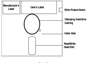
Floppy disk is made of Mylar plastic material coated with magnetic oxide and enclosed in a protective jacket. In oval access hole is made on jacket to provide contact between R/W head and diskette.
Manufacturers
Label Users Label Write Protect Notch
[image:41.612.134.542.460.721.2]WRITE PROTECTED NOTCH
When it is closed information cannot be written. Floppy reading is possible when it is open, both reading and writing is possible.
INDEX HOLE
Index hole is used to identify the starting sector of any track.
DRIVE HUB
Sits on drive hub, so that diskette rotates whenever motor in the drive rotates.
READ/WRITE HEAD SLOT
This is used for the movement of the Read/Write head over the disk surface.
USER’S LABEL
It is the space provided for user to write any name, which indicates the contents of diskette.
FLOPPY DISK DRIVE
The Floppy diskette surface is logically divided into a fixed number of tracks concentric circles as shown in figure. The number of tracks in one surface of a diskette are 77,40,80 for 8 inch, 51/
4 inch, double density diskette respectively. Reading or writing takes place on specified tracks and not in between the tracks.
The Read/Write head are mounted on a common assembly in FDD. The head assembly moves to and fro in steps between outermost track and innermost track. It can move in both directions(towards the centre) and backwards(towards outermost the centre). The subsequent tracks are numbered sequentially.
The diskette having a small hole called index hole. This is reference point indicating the beginning of a track. When the diskette rotates, the index sensor in FDD senses the passing of index hole. Initial writing of any track is done after the index hole is sensed.
Each track is divided into number of sectors. The number of sectors in a track depends on the size and recording method used. In each sector, a fixed number of data bites are written.
Depending on sector organization, the floppy disk is classified in to two types 1. Hard sectored floppy diskette.
2. Soft sectored floppy diskette.
4.3.1 Hard Sectoring
4.3.2 Soft Sectoring
The number of sector on each track is chosen by the software. This number can be varied for a given diskette by various software programs. There are no physical holes on the diskette for sector information.
4.3.3 Data Recording
Data is written on track bit by bit. The read/write head reads or writes on the diskette using standard electromagnetic recording technique. One head writes on the top surface of the diskette and the other head writes on the bottom surface.
4.3.4 FM technique
Each data bit is recorded in a cell along with clock pulse. Clock pulse is written for each data cell. The cell length is 4 msec on the magnetic medium; the information is stored in “FLUX Reversals” on the media and not in amplitude or direction of magnetization. Each bit is recorded as a flux change.
4.3.5 MFM technique ( Modified Frequency Modulation )
For MFM technique, the cell duration is 2msec here pulse is not written for each data cell. It is present only when data is on present & previous cell.
The diskette is logically divided into a fixed number of tracks or concentric circles. Reading or writing takes place only on these circles & not between tracks. There is a small hole punched on the diskette near the centre called index hole. This is reference point for start of track.
4.4 FDC SYSTEM INTERFACE
AEN : To enable selection of I/O ports only during CPU bus cycle.
A0 - A9 : Only 10 LSBs of the address bus, A9 - A0 are decoded by FDC logic. The remaining six MSB are ignored.
IOW : This signal becomes active when CPU or DMA controller conducts an I/O read cycle.
D0-D7 : Bi-directional data bus.
DRQ2 : When FDC is ready to transfer 1 byte of data to memory or FDC is ready to read 1 byte of data from memory, it is generated.
DACK2 : Issued by DMA controller when it performs DMA cycle in response to DRQ2.
T/C : This signal is issued by DMA controller to indicate that byte count for DMA channel is zero.
IRQ6 : The FDC generates this signal, when it has completed execution of command.
Reset Drive : Issued by motherboard circuit during reset sequence.
4.5 FDD INTERFACE
DOS can be loaded only from drive 0 since BIOS excepts the diskette there only. Hence FDD after the twist in the cable becomes drive 0.
4.6 FLOPPY DISK DRIVE ALIGNMENT
The alignment adjustment in the IBM drives set the positioning of the read/write head correctly over the track on the disk, adjust the disk stop guide, adjust index hole sensor or adjust the hub that fits in the disk. A check is also made of the head azimuth compared with the disk track. These Procedures require special equipment including dual trace oscilloscope, disk management tools & special alignment disks.
4.6.1 Track 00 Adjustment
Adjustment of the track 00 properly positions drive read/write head over disk track 0. A stop screw holds the switch at a setting fixed at track 0. This switch setting rarely needs adjustment if it does the drive will not read at all. If the system does not boot and you think that Track-0 alignment may be out of tolerance, then start by setting the radial head alignment first.
TOOLS REQUIRED
l Flathead Screwdriver l Philips head Screwdriver l Protective Pad
l Adequate lighting
l Tray to hold loose Screws
1. Turn OFF computer
2. Disassemble the computer
3. Disconnect the disk drive data cable
4. Remove the silverhead screw holding to chassis
5. Gently pull drive forward about 2 inches out from the front chassis 6. Disconnect the power supply cable from back of PCB
7. Remove the drive from chassis.
8. Set drive aside towards you to adjust the screw at the back of drive. 9. Connect power supply cable again &
10. Reconnect data cable
11. Insert program disk in the drive(diagnostic) 12. Loosen the screw from bracket
13. Turn the screw in the clockwise till you get the message track 0 o.k.
14. If OK insert the drive inside the chassis, put a copy of program disk in drive, verify correct operation.
4.7 FORMATTING FLOPPIES
into a number of sectors of fixed length, track contains the same number of sectors.
The formatted storage capacity of the diskette is less than unformatted storage capacity. The disk space that must be used to store location, identification & timing of information on the disk in order to let the system then at all time which track & sector is reading. It reserves first track Track0 to identify the type of information found on other track.
In a PC, DOS organizes 9 sectors, on a track with 512 bytes of data, each sector. Each ID field contains address of the sector. Data field contains actual data. ID field is seven bit long. The ID address mark, cylinder number, Head number, sector length, CRC bytes there are contains of ID field. The bad track is identified by writing hex FF in ID field.
Formatting a diskette removes previous data stored in it and writes the data in ID field.
4.8 Making a Diskette DOS Bootable
To make the diskette bootable in DOS, following steps can be taken:
1. Using the FORMAT command with /S switch ( syntax FORMAT A: /S ) 2. Using the SYS external command ( syntax SYS A: )
3. Using utilities like Norton Disk Doctor, PC Tools, XT Gold etc.
ASSIMILATION EXERCISE
Q.1 How is read/write head for a disk drive moved into position over a specified track ? Q.2 What additional information besides the actual data is recorded on each track of a
softsectored floppy disk ?
Q.3 Describe the purpose of CRC bytes included with each block of data recorded on the disk ?
Q.4 Why must clock bit be recorded alongwith data bits on floppy disk ?
Q.5 Under what condition will clock pules be inserted in a bit cell when recorded data on a disk in MFM format ?
Q.6 For a disk using MFM encoding and IBM Standard format with 26 sectors of 256 bytes each, what percentage of disk capacity is lost due to formatting ? What is this percentage if eight sectors of 1024 bytes are used instead ?
Q.7 A double-sided floppy disk with 40 tracks per side has how many cylinders ? Q.8 What is interleaving sector ? What is interleave factor ?
HARD DISK DRIVES
COMPETENCY OBJECTIVES
The objective of this Chapter is to make students understand the types of Hard Disks standards available, its installation. At the end of this section, a student should be able to
:-v Understand the geometry of a Hard disk.
v Differentiate between the various types of Hard disks.
CHAPTER - 5
HARD DISK DRIVE
5.0 TYPES OF HARD DISK
Hard disks been very effective input/output device for computer. It is secondary or auxiliary memory.
Depending on the type of interface, HDD can be classified as
1. ST506 2. ESDI drive 3. IDE Drive 4. SCSI Drive
1. ST 506
ST506 are traditional types found in PC’s, they are reliable, and they suffer from slow data transfer rate. The advantage is almost all ROM BIOS directly supports this. This interface standard is from Seagate Technology.
2. ESDI Standards
Enhanced Small Drive Interface. The advantage is ESDU control devices are on HDD itself. So ESDI can’t be used with ST506/412 driver. But uses the same data and control cable.
ESDI are formatted for 34/35 sectors/track. So transfer speeds of 10MBPS can be achieved.
3. IDE drives
4. SCSI Standards
It is Small Computer System Interface used for attaching various types of devices to a computer system. SCSI is an 8-bit parallel bus that can support up to 8 devices.
SCSI is capable of data transfer rates up to 33 MBPS.
5.1 GEOMETRY OF HARD DISK
5.1.1 Construction of Hard Disk
In the case of hard disk the recording surfaces are permanently encased in a metal enclosure to shield them from dust and dirt. All that is visible is a hard disk drive, a metal box with some circuitry on it.
5.1.2 Platters
To increase the drive capacity, virtually all hard disk drives contain two or more magnetic disks. The disks are referred as platters. They are mounted around an axis called spindle. All the platters turn together at constant speed of 3600 RPM. The motor that turns the spindle that may be built into spindle, or it may be reside below this spindle.
Both the sides of platters hold the data. Each side of a platter has one read/write head. The heads are connected to comb like arm, that moves all heads together.
The heads are to stay close to the platters(several microns) without touching because they actually flyover the surface on a cushion of air created by disk fast rotation. The heads slowly lift off when the drives start up and they gently land over when power is shut off. This concept of heads above disk surface prevents the head from weaving out the magnetic coating.
5.1.3 Stepper Motor Actuator
Stepper Motor rotates in terms of fixed steps as per the digital information fed to the motor. The distance the motor turns, for each step is fixed by the construction of the motor.
5.2 HARD DISK FORMAT
The capacity of a hard disk depends on the number of cylinders, number of surfaces,number of heads and recording density. The DOS organizes tracks into 17 Sectors and 512 bytes/ sector.
5.2.1 Boot Sector
GAP 1
The minimum length of GAP 1 is 12 bytes.
5.2.2 SYNC
The SYNC field is created before each addressable record. Its length should be sufficient to match the look up characteristic.
GAP 3
The GAP 3 is created after each sector. This acts as protection against overwriting on adjacent sector when created a new sector data due to spindle speed variations.
GAP 4
The GAP 4 is created against the end of last sector in each track so that last sector does not overflow beyond the index due to speed variation.
DISPLAY PARTITION INFORMATION
Current Fixed disk drive : 1
Partition Status Type Volume label Mbytes System Usage
C:1 A PRI DOS STVBEAR 505 FAT16 100%
Total disk space is 505 Mbytes Press Esc to continue
The FDisk Program enables you to manipulate the disk partition while working with DOS. If you are working with another operating system then FDisk enables you to create or delete DOS based partition.
If you need to resize DOS partition, you must back up the contents of the partition, delete the partition, create a new partition if(with FORMAT) and reload the data from your backup disk.
DOS divides each disk into two parts: System part, used for DOS’s record keeping, data part, where the files are stored. The system portion has three parts, boot record, File Allocation Table & root directory.
5.2.3 Boot record
Boot Record is always very first data on the disk. It is used to hold a short program that begins the process of starting DOS.
The File Allocation Table(FAT)
5.2.4 The Root Directory
The Directory works as a simple table of 32 byte entries that describe the files on disk.
5.3 PHYSICAL & LOGICAL FORMATTING
The formatting of disk required two steps Physical & Logical Formatting.
Physical formatting is sometimes called low level formatting - involves creation of physical sectors on a disk. The sectors are created, complete with their address markings and with data portion of the Sector established and filled in with dummy data. A new hard disk is almost always physically formatted when you buy it.
5.4 PARTITIONING
Partitioning is a procedure, which divides the hard disk into multiple sections or partitions. Each partition is compressed of several cylinders or tracks. Different operating systems may be stored on different Partitions.
Partitioning the Disk
Partitioning means dividing into parts. Most of your disk is divided into Partitions in which you can store files of information. To partition on hard disk, DOS has a program called FDISK, which can change and Partition data. FDISK can list upto four partitions. Partition in the list has a starting and ending location & size in disk cylinders.
5.5 HANDLING OF HARD DISK
Hard drives are sealed units. This is necessary because of microscopic spacing of the heads over the rotating medium. When the computer is operating the read/write head of hard drive are “flying” on a cushion of last moving air, just above rotating disk. The air carried along with rotating at the normal 3,600 RPM: the head may damage the coating on the disks & cause catastrophic failure. This is called ‘head crash’, for this reason, NEVER MOVE OR JERK A COMPUTER WHILE IT IS IN OPERATION if it has hard disk installed.
A hard disk can be operated in horizontal position.
A few tips and tricks :
l Do not make too complicated directory l Use CHKDSK regular.
l Try backing up data regularly. This is a good habit to recover data in case of hard disk failure.
l Always keep a bootable diskette in the same version as the hard disk .
Use latest Antivirus Program to check the hard disk regularly.The following table gives the hard disk parameters for PC/AT and PS/2 system.
Type Cylinder Hd WPC Ctrl Lz S/T MB
1 306 4 128 00h 305 17 10.65
2 615 4 300 00h 615 17 21.41
3 615 6 300 00h 615 17 32.12
4 4940 8 512 00h 940 17 65.45
5 940 6 512 00h 940 17 49.09
6 615 4 65,535 00h 615 17 21.41
7 462 8 256 00h 511 17 32.17
8 733 5 65,535 00h 733 17 31.90
9 900 15 65,535 00h 901 17 117.50
10 820 3 65,535 00h 820 17 21.42
11 855 5 65,535 00g 855 17 37.21
12 855 7 65,535 00h 855 17 52.09
13 306 8 128 00h 319 17 21.31
14 733 7 65,535 00h 733 17 44.66
15 0 0 0 00h 0 0 0
16 612 4 0 00h 663 17 21.31
17 977 5 300 00h 977 17 42.52
18 977 7 65,535 00h 977 17 59.53
19 1024 7 512 00h 1023 17 62.39
20 733 5 300 00h 732 17 31.90
21 733 7 300 00h 732 17 44.66
22 733 5 300 00h 733 17 31.90
23 366 4 0 00h 336 17 10.54
24 612 4 305 00h 663 17 21.31
25 306 4 65,535 00h 340 17 10.65
26 612 4 65,535 00h 670 17 21.31
27 698 7 300 20h 732 17 42.53
28 976 5 65.535 20h 977 17 42.48
29 306 4 65,535 00h 340 17 10.65
30 611 4 65,535 20h 663 17 21.27
31 732 7 65,535 20h 732 17 44.60
32 1023 5 65,535 20h 1023 17 44.52
33 614 4 65,535 20h 663 25 31.44
34 775 2 65,535 20h 900 27 21.43
35 921 2 65,535 20h 1000 33 31.12
36 402 4 65,535 20h 460 26 21.41
37 580 6 65,535 20h 640 26 46.33
38 845 2 65,535 20h 1023 36 31.15
39 969 3 65,535 20h 1023 36 42.52
40 531 4 65,535 20h 532 39 42.41
42 654 2 65,535 20h 674 32 21.43
43 923 5 65,535 20h 1023 36 85.06
44 531 8 65,535 20h 532 39 84.82
45 0 0 0 0 0 0 0.00
46 0 0 0 0 0 0 0.00
47 0 0 0 0 0 0 0.00
Type = Drive type number cyls = Total cylinders Heads = Total heads
WPC = Write Precompensation starting cylinder ctrl = Control byte : Values
Bit 0 = 01h not used Bit 1 = 02h not used Bit 3 = 04h not used
Bit 3 = 08h more than 8 heads Bit 4 = 10h not used
Bit 5 = 20 h OEM defect map Bit 6 = 40h disable disk retries. Bit 7 = 80h disable disk refries.
47 = Landing Zone cylinder for head parking ST = Number of sectors per track.
MB = Drive capacity in millions of bytes.
ASSIMILATION EXERCISE
Q.1 What are signal sequence while reading data from Hard Disk Drive ? Q.2 What is the use of write precompensation circuitry in Hard Disk ? Q.3 What is size of sector buffer & why it is used ?
Q.4 What are two functions performed by HDC BIOS ROM ? How presence of HDC or absence is determined ?
Q.5 What are the parameter to determine the capacity of hard disk ? Q.6 What is Boot Sector ? Which information is stored in it ?
Q.7 Why must hard disk be operated in a dust free environment ?
Q.8 Two terms often encountered in hard disk system manuals are cylinder & partition. Define & tell the difference between these two terms.
Q.9 A hard disk rotates at 3600 RPM & has an average seek time 35 ms. What is the average total access time, including rotational latency ?
SWITCH MODE POWER SUPPLY
COMPETENCY OBJECTIVES
The objective of this Chapter is to introduce the students to SMPS operation. At the end of this section, a student should be able to
:-v Understand functional operation of SMPS.
v Differentiate between various functional Sub-blocks.
CHAPTER - 6
SWITCH MODE POWER SUPPLY
6.1 INTRODUCTION
The power supply is the important element of any piece of electrical or electronic equipment. The successful operation of any piece of electrical or electronic equipment depends upon overall functioning of the power supply.
The primary function of any power supply is to provide a predetermined constant output voltage when the input voltage and/or output current vary widely & there is possibility of change in operating temp. The degree to which power supply provides a constant output voltage.
6.2 FUNDAMENTALS OF SWITCH MODE POWER SUPPLY
In contrast with linear DC regulated power supply, a switching power supply employs transistors which operates as a switch, either “ON” or “OFF”. The output voltage is controlled by controlling the “ON” and “OFF” Duration’s. This is called switch mode DC - DC conversion.
In the above figure, the average output voltage Vo is controlled employing switching at a frequency and adjusting the “ON” Duration to Control the output.
The above method is called PULSE WIDTH MODULATION switching.
The switching regulators can be of the free running type or driven type. The output voltage is used to generate a PWM signal, which is used to drive the regulator Switch such that the output voltage is maintained at predetermined level. This PWM signal can have one of the following characteristics.
i) Fixed ON Period and variable OFF Period.
ii) Variable ON and OFF Periods with fixed frequency. iii) Fixed OFF period and variable ON Period.
To enhance the Power capability, the above regulation are usually connected in parallel, and are operated in phase shift mode to reduce the EMI and problems of electromagnetic screening. To improve the performance characteristics (such as regulation, transient response etc.), the feedback control loop of the above regulation is modified to sense the AC changes besides DC changes on the output voltage and changes in the input voltages.
6.2.1 Block Diagram of SMPS
6.2.1 AC Filter
6.2.3 Rectifier
The filtered AC main voltage is rectified and converting into pulsating DC by a bridge rectifier. This pulsating DC is then filtered by a capacitor filter to get a pure DC.
6.2.4 Push Pull Converter
A Push pull converter is used to switch the DC voltage ON/OFF to the primary of a high frequency transformer to get a train frequency pulses at the output of the transformer.
The switched voltage at the secondary of the transformer is rectified and filtered to get a pure DC voltage at the output. The 5V DC voltage is sampled & fed to PWM IC. This voltage is compared with the reference voltage and depending on whether the output voltage is greater/ lesser than input voltage, the PWM IC controls the OFF/ON periods of the switching transistors to maintain the output voltage.
6.2.5 Schematic Circuit Study of Typical SMPS
The AC mains voltage is applied to the circuit through fuse ‘f’, Resistor R used to prevent the sudden inrush of current from AC main when the Power supply is switched ON. The inductors L1 and L2 prevent any high frequency signals to enter into circuit.
L1 & L2 are two inductors wound on the same core. The magnetic field that is produced are equal in both lines but opposite in direction. Therefore, they cancel out each other. Thus, filter action is obtained. This arrangement also provides very high inductance to common mode signals.
The filtered AC line voltage is then rectified and converted to DC by a bridge rectifier. Thus obtained signal is not a pure DC, but has a very high ripple content in it. This is called pulsating DC. This is then filtered by a capacitor to get a pure DC voltage. C3 and C4 are filter capacitors, which are in series across the bridge rectifier output. Thus the total dc voltage is divided and half of the voltage appears across C1 and other half across C2.
6.2.6 Push Pull Amplifier
capacitor’s C1 & C2.
In the half wave bridge configuration the power transformer has one side connected to a floating voltage potential created by the series capacitor C1 & C2 which has a value at V/2 150V DC at junction of Q1 emitter & Q2 collector through a series capacitance C3. When Q1 turns ON, the transformer goes to positive bus generating (150 V) voltage pulse. When Q1 turns off & Q2 turns on the polarity at the transformer primary reverses since it is now connected to the negative bus generating negative pulse of 150V. The turn ON & turn OFF action of Q1 & Q2 will generate a 300 V peak to peak square wave.
6.2.7 Typical Output Section
Choke coil
6.2.8 Control Section
Majority of today’s switching power supplies are of the pulse width modulated type. The technique varies the conduction time at the switching transistor during the ON period to control and regulate the O/P voltage to a predetermined level.
6.2.8.1 PWm Section
The fixed frequency PWM technique is used. In this system, a square wave pulse is normally generated to drive the switching transistor ON or OFF. By varying the width of the Pulse, the conduction time of the transistor is varied, thus regulating output voltage. The PWM control circuit may be single ended capable of driving a single transistor converter; or dual channel PWM circuit is used.
6.2.9 Integrated PWM controller :
The Fig. No. 6-7 shows the basic building of PWM controller & the waveform is as shown in Fig. No. 6.8 circuit functions as OPAMP compares the feedback signal from the output of the Power supply to fixed reference voltage Vref. The error signal is applied and fed into inverting input of a comparator. The non-inverting input accepts the sawtooth waveform with a linear slope, generated by a fixed frequency oscillator. The oscillator output is used to toggle a flip-flop, producing square wave output Q & Q
The comparator square wave output and the flip flop output are both used to drive AND gates, enabling each output when both inputs to the gate are high. The result is a variable duty cycle pulse train at channel A & B fig. 6.8 waveform shows output pulse width modulated when the error signal changes its output (shown in dotted lines). The output of PWM controller are externally buffered to drive main power switching transistors.
6.3 THE FAN
A cooling fan is mounted on the cabinet of the supply. The air into the supply and air sucked in by the fan carries off the heat generated by components of Power supply, thereby maintaining the Power supply at room temperature. The supply for the fan is 12V.
6.3 POWER SUPPLIES USED IN P.C.
A PC needs power at two different voltage levels, both positive and negative Polarities. +5V DC, +12V DC, -5V DC, -12V DC. The power supply has to provide power at all these four voltages. Most of the power needed by electronic circuitary is +5V DC, +12V DC voltages are required by DC motors.
The total power requirements of a PC depends upon components within it. Each component will draw a certain quantity of current at each of the supply voltages it uses. Some components will draw a certain quantity of current depending on what they are doing.
Typical PC power supply rating :
Voltage PC (65W)
Current (A) XT Current (A) Current (A)AT (200W)
Min Max Min Max Min Max
+ 5 (± 5%) 1.5 7.0 2.5 15.6 7.0 19.8
+12 (±5%) 0.3 2.0 1.0 4.2 0.5 7.3
- 5 (±10%) 0.06 0.3 -- 0.3 -- 0.3
-12 (±10%) 0.06 0.3 -- 0.3 -- 0.3
6.4 TROUBLESHOOTING
Before opening the system box and going into the check-up of internal circuitary it is always a good practice to follow the following procedures.
1) Check input voltage. 2) Check mains supply.
3) Check Power Cable plugged is fully. 4) Test fuse and cable continuity.
5) Check operation of switch (Mechanically by inspection electrically by disconnecting from mains & then measuring the resistance across line & neutral terminals of main plug while operating the switch the resistance should be high with switch off, low with it on).
6) Check output voltages and Power good signal from Power supply using volt-ohm meter.
1) VOLTAGE IS LESS/MORE AT THE OUTPUT
This problem may be due to fault in feedback or in PWM IC, the IC compares it’s reference voltage with improper one, thereby resulting in increase / decrease of voltage at the output. The Problem may also be due to improper reference generated to IC.
To correct this problem check whether the reference voltage is at 5V, if no, check for the power supply to the IC. If this is OK then the IC is faulty, replace the IC. If the IC is OK, check for the feedback loop, check the resistors in feedback path and replace the faulty one.
2) VERY HIGH RIPPLE IN THE OUTPUT
This problem is due to faulty capacitor, the capacitor may dry up their resulting in inefficient filtering of the rectified voltage. Replace the capacitor to get a good ripple free DC voltage.
The Power supply switched ON for a very brief period of time and then switches OFF.
The problem is either due to a short in the circuit resulting in a large current flowing in the circuit thereby IC switches of the power supply or it may be due to fault in the current sense circuit. Check for the faulty diodes in the output circuit & capacitors.
Check for the components that for the current sense circuit. Also check the reference voltage of IC.
3) THE POWER SUPPLY DOES NOT SWITCH ON AT ALL
First of all check whether DC voltage across the capacitors C1 & C2 is at the required level or not. If their is no voltage there is some problem in the line filter/rectifier. If it is OK, it is the problem in the rest of circuitry. The only way to find out the problem is to check the components individually in push pull, output & IC. Check the transistors Q1 & Q2, the driving transistors T1 & T2 rectifying diodes at the output, the driving transformer & the capacitor, resistors connected to the oscillator of PWM.
One way to check the IC is to isolate the output of Pin11, Pin9 of the IC with the power supply circuit. Power the IC with an external +12V supply and give a +5V to the feedback circuit. If the IC oscillates giving pulses at the output IC is OK.
DIAGRAM 3
ASSIMILATION EXERCISE
Q.1 Explain the PWM Principle ? How it is used to control the output voltage ? Q.2 What are advantages of SMPS over linear Power Supply ?
Q.3 Explain in detail AC filter section ?
Q.4 How to troubleshoot the following problem ? +5v is coming exactly the +5.0 volts
but +12V regulated DC output is coming out to be +9.6 Volts
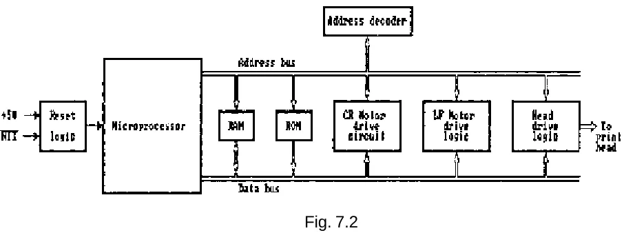
PRINTERS
COMPETENCY OBJECTIVES
The objective of this Chapter is to make the students understand the operation and types of Printers. At the end of this section, a student should be able to
:-v Distinguish between various types of printers based on their operation.
v Understand the mechanism of a Dot-Matrix printer.
CHAPTER - 7
PRINTERS
7.0 TYPES OF PRINTERS
Printers are broadly classified into two types
IMPACT : Some of the printer body makes contact with paper so that make impression or character formation
NON-IMPACT : There is no physical contact of the head with paper or ribbon.
IMPACT PRINTERS : Daisy Wheel Printer Dot Matrix Printer 1) 80 Column 2) 132 Column
NON IMPACT PRINTER : Ink Jet Printers Laser Printer Thermal Printer
7.1 PRINTER