Power Supply Circuits
In Brief . . .
Page
Linear Voltage Regulators . . . 4.2–2 Fixed Output. . . 4.2–2 Adjustable Output . . . 4.2–4 Micropower Voltage Regulators for Portable Applications . . . 4.2–5 80 mA Micropower Voltage Regulator . . . 4.2–5 120 mA Micropower Voltage Regulator . . . 4.2–6 Micropower Voltage Regulator for
External Power Transistor. . . 4.2–6 Low Noise 150 mA Low Drop Out (LDO) Linear
Voltage Regulator. . . 4.2–7 Micropower smallCAP Voltage Regulators with
On/Off Control. . . 4.2–8 Special Regulators . . . 4.2–9 Voltage Regulator/Supervisory . . . 4.2–9 SCSI Regulator . . . 4.2–13 Switching Regulator Control Circuits . . . 4.2–14 Single–Ended. . . 4.2–14 Single–Ended with On–Chip Power Switch. . . 4.2–16 Very High Voltage Single–Ended with
On–Chip Power Switch. . . 4.2–17 Double–Ended . . . 4.2–17 CMOS Micropower DC–to–DC Converters . . . 4.2–19 Synchronous Rectification DC/DC Converter
Programmable Integrated Controller. . . 4.2–21 Easy Switcher Single–Ended with On–Chip
Power Switch . . . 4.2–23 Single–Ended GreenLine Controllers . . . 4.2–25 Very High Voltage Switching Regulator . . . 4.2–27 High Voltage Switching Regulator. . . 4.2–29 Critical Conduction SMPS Controller . . . 4.2–30 High Voltage Switching Regulator. . . 4.2–31 Special Switching Regulator Controllers . . . 4.2–32 Dual Channel . . . 4.2–32 Universal Microprocessor Power Supply . . . 4.2–32 Power Factor . . . 4.2–33 Supervisory Circuits . . . 4.2–36 Overvoltage Crowbar Sensing. . . 4.2–36 Over/Undervoltage Protection . . . 4.2–36 Micropower Undervoltage Sensing. . . 4.2–37 Micropower Undervoltage Sensing with
Programmable Output Delay . . . 4.2–38 Undervoltage Sensing. . . 4.2–39 Universal Voltage Monitor . . . 4.2–40 Battery Management Circuits . . . 4.2–41 Battery Charger ICs. . . 4.2–41 Battery Pack ICs . . . 4.2–43 Power Supply and Management IC for Handheld
Electronic Products . . . 4.2–48 MOSFET/IGBT Drivers. . . 4.2–50 High Speed Dual Drivers . . . 4.2–50 Single IGBT Driver. . . 4.2–50
In most electronic systems, some form of voltage regulation is required. In the past, the task of voltage regulator design was tediously accomplished with discrete devices, and the results were quite often complex and costly. Today, with bipolar monolithic regulators, this task has been significantly simplified. The designer now has a wide choice of fixed, low VDiff and adjustable type voltage regulators. These devices incorporate many built–in protection features, making them virtually immune to the catastrophic failures encountered in older discrete designs.
The switching power supply continues to increase in popularity and is one of the fastest growing markets in the world of power conversion. They offer the designer several important advantages over linear series–pass regulators. These advantages include significant advancements in the areas of size and weight reduction, improved efficiency, and the ability to perform voltage step–up, step–down, and voltage–inverting functions. Motorola offers a diverse portfolio of full featured switching regulator control circuits which meet the needs of today’s modern compact electronic equipment.
Linear Voltage Regulators
Fixed Output
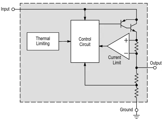
These low cost monolithic circuits provide positive and/or negative regulation at currents from 100 mA to 3.0 A. They are ideal for on–card regulation employing current limiting and thermal shutdown. Low VDiff devices are offered for battery powered systems.
[image:2.612.48.551.166.690.2]Although designed primarily as fixed voltage regulators, these devices can be used with external components to obtain adjustable voltages and currents.
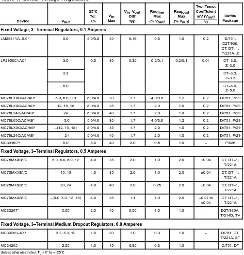
Table 1. Linear Voltage Regulators
Device Vout
25°C Tol.
±%
Vin Max
Vin–Vout Diff. Typ.
Regline Max (% Vout)
Regload Max (% Vout)
Typ. Temp. Coefficient mV (Vout)
°C
Suffix/ Package
Fixed Voltage, 3–Terminal Regulators, 0.1 Amperes
LM2931*/A–5.0* 5.0 5.0/3.8 40 0.16 0.6 1.0 0.2 D/751,
D2T/936, DT, DT–1, T/221A, Z
LP2950C*/AC* 3.0 0.5 30 0.38 0.2/0.1 0.2/0.1 0.04 DT–3.0,
Z–3.0
3.3 DT–3.3,
Z–3.3
5.0 DT–5.0,
Z–5.0
MC78LXXC/AC/AB* 5.0, 8.0, 9.0 8.0/4.0 30 1.7 4.0/3.0 1.2 0.2 D/751, P/29
MC78LXXC/AC/AB* 12, 15, 18 8.0/4.0 35 1.7 2.0 1.0 0.2 D/751, P/29
MC78L24C/AC/AB* 24 8.0/4.0 40 1.7 2.0 1.0 0.2 D/751, P/29
MC79L05C/AC/AB* –5.0 8.0/4.0 30 1.7 4.0/3.0 1.2 0.2 D/751, P/29
MC79LXXC/AC/AB* –(12, 15, 18) 8.0/4.0 35 1.7 2.0 1.0 0.2 D/751, P/29
MC79L24C/AC/AB* –24 8.0/4.0 40 1.7 2.0 1.0 0.2 D/751, P/29
MC33160** 5.0 5.0 40 2.0 0.8 1.0 – P/626
Fixed Voltage, 3–Terminal Regulators, 0.5 Amperes
MC78MXXB*/C 5.0, 6.0, 8.0, 12 4.0 35 2.0 1.0 2.0 ±0.04 DT, DT–1,
T/221A
MC78MXXB*/C 15, 18 4.0 35 2.0 1.0 2.0 ±0.04 DT, DT–1,
T/221A
MC78MXXB*/C 20, 24 4.0 40 2.0 0.25 2.0 ±0.04 DT, DT–1,
T/221A
MC79MXXB*/C –(5.0, 8.0, 12, 15) 4.0 35 1.1 1.0 2.0 –0.07 to
±0.04 DT, DT–1,T/221A
MC33267* 5.05 2.0 40 0.58 1.0 1.0 – D2T/936A,
T/314D, TV
Fixed Voltage, 3–Terminal Medium Dropout Regulators, 0.8 Amperes
MC33269–XX* 3.3, 5.0, 12 1.0 20 1.0 0.3 1.0 – D/751, DT,
T/221A, ST
MC34268 2.85 1.0 15 0.95 0.3 1.0 – D/751, DT
Unless otherwise noted, TJ = 0° to +125°C * TJ = –40° to +125°C
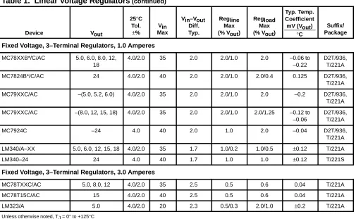
Table 1. Linear Voltage Regulators
(continued)Device
Suffix/ Package Typ. Temp.
Coefficient mV (Vout)
°C Regload
Max (% Vout) Regline
Max (% Vout) Vin–Vout
Diff. Typ. Vin
Max 25°C
Tol.
±% Vout
Fixed Voltage, 3–Terminal Regulators, 1.0 Amperes
MC78XXB*/C/AC 5.0, 6.0, 8.0, 12, 18
4.0/2.0 35 2.0 2.0/1.0 2.0 –0.06 to
–0.22
D2T/936, T/221A
MC7824B*/C/AC 24 4.0/2.0 40 2.0 2.0/1.0 2.0/0.4 0.125 D2T/936,
T/221A
MC79XXC/AC –(5.0, 5.2, 6.0) 4.0/2.0 35 2.0 2.0/1.0 2.0 –0.2 D2T/936,
T/221A MC79XXC/AC –(8.0, 12, 15, 18) 4.0/2.0 35 2.0 2.0/1.0 2.0/1.25 –0.12 to
–0.06
D2T/936, T/221A
MC7924C –24 4.0 40 2.0 1.0 2.0 –0.04 D2T/936,
T/221A
LM340/A–XX 5.0, 6.0, 12, 15, 18 4.0/2.0 35 1.7 1.0/0.2 1.0/0.5 ±0.12 T/221A
LM340–24 24 4.0 40 1.7 1.0 1.0 ±0.12 T/221S
Fixed Voltage, 3–Terminal Regulators, 3.0 Amperes
MC78TXXC/AC 5.0, 8.0, 12 4.0/2.0 35 2.5 0.5 0.6 0.04 T/221A
MC78T15C/AC 15 4.0/2.0 40 2.5 0.5 0.6 0.04 T/221A
LM323/A 5.0 4.0/2.0 20 2.3 0.5/0.3 2.0/1.0 ±0.2 T/221A
Unless otherwise noted, TJ = 0° to +125°C * TJ = –40° to +125°C
[image:3.612.66.571.46.357.2]** TA = –40° to +85°C
Table 2. Fixed Voltage Medium and Low Dropout Regulators
Device Vout
25°C Tol.
±% IO (mA)
Max Vin Max
Vin–Vout Diff. Typ.
Regline Max (% Vout)
Regload Max (% Vout)
Typ. Temp. Coefficient mV (Vout)
°C
Suffix/ Package
Fixed Voltage, Medium Dropout Regulators
MC33267* 5.05 2.0 500 40 0.58 1.0 1.0 – D2T/936A,
T/314D, TV
MC34268 2.85 1.0 800 15 0.95 0.3 1.0 D/751, DT
MC33269–XX* 3.3, 5.0, 12 20 1.0 D/751, DT,
T/221A, ST/318E
Fixed Voltage, Low Dropout Regulators
LM2931*/A* 5.0 5.0/3.8 100 37 0.16 1.12 1.0 ±2.5 D/751,
D2T/936A, DT, DT–1, T/221A, Z
LP2950C*/AC* 3.0 1.0/0.5 100 30 0.38 0.2/0.1 0.2/0.1 0.2 DT–3.0,
Z–3.0
3.3 DT–3.3,
Z–3.3
5.0 DT–5.0,
Table 2. Fixed Voltage Medium and Low Dropout Regulators
(continued)Device
Suffix/ Package Typ.
Temp. Coefficient mV (Vout)
°C Regload
Max (% Vout) Regline
Max (% Vout) Vin–Vout
Diff. Typ. Vin
Max IO
(mA) Max 25°C
Tol.
±% Vout
Fixed Voltage, Low Dropout Regulators
LP2951C*/AC* 3.0 1.0/0.5 100 28.75 0.38 0.04/0.02 0.04/0.02 ±1.0 D–3.0/751,
DM–3.0/ 846A, N–3.0/626
3.3 D–3.3/751,
DM–3.3/ 846A, N–3.3/626
5.0 D/751,
DM/846A, N/626
LM2935* 5.0/5.0 5.0/5.0 500/10 60 0.45/0.55 1.0 1.0 – D2T/936A,
T/314D, TH, TV Unless otherwise noted, TJ = 0° to +125°C
* TJ = –40° to +125°C
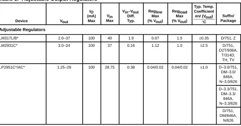
Adjustable Output
Motorola offers a broad line of adjustable output voltage regulators with a variety of output current capabilities. Adjustable voltage regulators provide users the capability of stocking a single integrated circuit offering a wide range of
[image:4.612.51.549.431.692.2]output voltages for industrial and communications applications. The three–terminal devices require only two external resistors to set the output voltage.
Table 3. Adjustable Output Regulators
Device Vout
IO (mA)
Max
Vin Max
Vin–Vout Diff. Typ.
Regline Max (% Vout)
Regload Max (% Vout)
Typ. Temp. Coefficient mV (Vout)
°C
Suffix/ Package
Adjustable Regulators
LM317L/B* 2.0–37 100 40 1.9 0.07 1.5 ±0.35 D/751, Z
LM2931C* 3.0–24 100 37 0.16 1.12 1.0 ±2.5 D/751,
D2T/936A, T/314D,
TH, TV
LP2951C*/AC* 1.25–29 100 28.75 0.38 0.04/0.02 0.04/0.02 ±1.0 D–3.0/751,
DM–3.0/ 846A, N–3.0/626 D–3.3/751,
DM–3.3/ 846A, N–3.3/626
D/751, DM/846A,
N/626 Unless otherwise noted, TJ = 0° to +125°C
Table 3. Adjustable Output Regulators
(continued)Device
Suffix/ Package Typ. Temp.
Coefficient mV (Vout)
°C Regload
Max (% Vout) Regline
Max (% Vout) Vin–Vout
Diff. Typ. Vin
Max IO
(mA) Max Vout
Adjustable Regulators
MC1723C# 2.0–37 150 38 2.5 0.5 0.2 ±0.033 D/751,
P/646
LM317M/B* 1.2–37 500 40 2.1 0.04 0.5 ±0.35 DT, DT–1,
T/221A
LM337M/B* –(1.2–37) 500 40 1.9 0.07 1.5 ±0.3 T/221A
MC33269* 1.25–19 800 18.75 1.0 0.3 0.5 ±0.4 D/751, DT,
T/221A, ST
LM317/B* 1.2–37 1500 40 2.25 0.07 1.5 ±0.35 D2T/936,
T/221A
LM337/B* –(1.2–37) 1500 40 2.3 0.07 1.5 ±0.3 D2T/936,
T/221A
LM350/B* 1.2–33 3000 35 2.7 0.07 1.5 ±0.5 T/221A
Unless otherwise noted, TJ = 0° to +125°C * TJ = –40° to +125°C
# TA = 0° to +70°C
Micropower Voltage Regulators for Portable Applications
80 mA Micropower Voltage Regulator
MC78LC00H, NTA = –30° to +80°C, Case 1213, 1212
The MC78LC00 series voltage regulators are specifically designed for use as a power source for video instruments, handheld communication equipment, and battery powered equipment.
The MC78LC00 series features an ultra–low quiescent current of 1.1 µA and a high accuracy output voltage. Each device contains a voltage reference, an error amplifier, a driver transistor and resistors for setting the output voltage. These devices are available in either SOT–89, 3 pin, or SOT–23, 5 pin, surface mount packages.
MC78LC00 Series Features:
• Low Quiescent Current of 1.1 µA Typical
• Low Dropout Voltage (220 mV at 10 mA)
• Excellent Line Regulation (0.1%)
• High Accuracy Output Voltage (±2.5%)
• Wide Output Voltage Range (2.0 V to 6.0 V)
• Output Current for Low Power (up to 80 mA)
• Two Surface Mount Packages (SOT–89, 3 Pin, or SOT–23, 5 Pin)
ORDERING INFORMATION
Device
Output Voltage
Operating
Temperature Range Package
MC78LC30HT1 3.0
T 30° 80°C
SOT 89 MC78LC33HT1 3.3
T 30° 80°C
SOT–89 MC78LC40HT1 4.0
T 30° 80°C
SOT–89 MC78LC50HT1 5.0
TA = –30°to +80°C MC78LC30NTR 3.0 TA = –30° to +80°C
SOT 23 MC78LC33NTR 3.3
SOT–23
MC78LC40NTR 4.0 SOT–23
MC78LC50NTR 5.0
Other voltages from 2.0 to 6.0 V, in 0.1 V increments, are available upon request. Consult factory for information.
2 Vin
1 Gnd
3 VO
Micropower Voltage Regulators for Portable Applications
(continued)
120 mA Micropower Voltage Regulator
MC78FC00H
TA = –30° to +80°C, Case 1213
The MC78FC00 series voltage regulators are specifically designed for use as a power source for video instruments, handheld communication equipment, and battery powered equipment.
The MC78FC00 series voltage regulator ICs feature a high accuracy output voltage and ultra–low quiescent current. Each device contains a voltage reference unit, an error amplifier, a driver transistor, and resistors for setting output voltage, and a current limit circuit. These devices are avail-able in SOT–89 surface mount packages, and allow construction of an efficient, constant voltage power supply circuit.
MC78FC00 Series Features:
• Ultra–Low Quiescent Current of 1.1 µA Typical
• Ultra–Low Dropout Voltage (100 mV at 10 mA)
• Large Output Current (up to 120 mA)
• Excellent Line Regulation (0.1%)
• Wide Operating Voltage Range (2.0 V to 10 V)
• High Accuracy Output Voltage (±2.5%)
• Wide Output Voltage Range (2.0 V to 6.0 V)
• Surface Mount Package (SOT–89)
ORDERING INFORMATION
Device
Output Voltage
Operating
Temperature Range Package
MC78FC30HT1 3.0
T 30° 80°C SOT 89 MC78FC33HT1 3.3
TA = –30°to +80°C SOT–89 MC78FC40HT1 4.0 TA = –30° to +80°C SOT–89 MC78FC50HT1 5.0
Other voltages from 2.0 to 6.0 V, in 0.1 V increments, are available upon request. Consult factory for information.
2 Vin
1 Gnd
3 VO
Vref
Micropower Voltage Regulator for External Power Transistor
MC78BC00NTA = –30° to +80°C, Case 1212
The MC78BC00 voltage regulators are specifically designed to be used with an external power transistor to deliver high current with high voltage accuracy and low quiescent current.
The MC78BC00 series are devices suitable for construct-ing regulators with ultra–low dropout voltage and output cur-rent in the range of several tens of mA to hundreds of mA. These devices have a chip enable function, which minimizes the standby mode current drain. Each of these devices con-tains a voltage reference unit, an error amplifier, a driver tran-sistor and feedback retran-sistors. These devices are available in the SOT–23, 5 pin surface mount packages.
These devices are ideally suited for battery powered equipment, and power sources for hand–held audio instru-ments, communication equipment and domestic appliances. MC78BC00 Series Features:
• Ultra–Low Supply Current (50 µA)
• Standby Mode (0.2 µA)
• Ultra–Low Dropout Voltage (0.1 V with External Transistor and IO = 100 mA)
• Excellent Line Regulation (Typically 0.1%/V)
• High Accuracy Output Voltage (±2.5%)
ORDERING INFORMATION
Device
Output Voltage
Operating
Temperature Range Package
MC78BC30NTR 3.0
T 30° 80°C SOT 23 MC78BC33NTR 3.3
TA = –30°to +80°C SOT–23 MC78BC40NTR 4.0 TA = –30° to +80°C SOT–23 MC78BC50NTR 5.0
Other voltages from 2.0 to 6.0 V, in 0.1 V increments, are available upon request. Consult factory for information.
2 Vin
1 Gnd 3 VO 4
Ext
Micropower Voltage Regulators for Portable Applications
(continued)
Low Noise 150 mA Low Drop Out (LDO) Linear Voltage Regulator
MC78PC00TA = –40° to +85°C, Case 1212
The MC78PC00 are a series of CMOS linear voltage regu-lators with high output voltage accuracy, low supply current, low dropout voltage, and high Ripple Rejection. Each of these voltage regulators consists of an internal voltage refer-ence, an error amplifier, resistors, a current limiting circuit and a chip enable circuit.
The dynamic Response to line and load is fast, which makes these products ideally suited for use in hand–held communication equipment.
The MC78PC00 series are housed in the SOT–23 5 lead package, for maximum board space saving.
MC78PC00 Series Features:
• Ultra–Low Supply Current: typical 35 mA in ON mode with no load
• Standby Mode: typical 0.1 mA
• Low Dropout Voltage: typical 0.2 V @ IOUT = 100 mA
• High Ripple Rejection: typical 70 dB @ f = 1 kHz
• Low Temperature–Drift Coefficient of Output Voltage: typical ±100 ppm/°C
• Excellent Line Regulation: typical 0.05%/V
• High Accuracy Output Voltage: ±2.0%
• Fast Dynamic Response to Line and Load
• Small Package: SOT–23 5 leads
• Built–in Chip Enable circuit (CE input pin)
• Similar Pinout to the LP2980/1/2 and MIC5205
ORDERING INFORMATION
Device
Operating
Temperature Range Package
MC78PC28NTR
T 40° 85°C SOT 23 MC78PC30NTR
TA = –40°to +85°C SOT–235 L d MC78PC33NTR TA = –40° to +85°C 5 Leads MC78PC50NTR
Other voltages are available. Consult your Motorola representative.
Block Diagram
1
VIN 5 VOUT
Vref
CE
3 2
GND CURRENT LIMIT
Micropower Voltage Regulators for Portable Applications
(continued)
Micropower smallCAP
Voltage Regulators with On/Off Control
MC33264D, DM
TA = –40° to +85°C, Case 751, 846A
The MC33264 series are micropower low dropout voltage regulators available in SO–8 and Micro–8 surface mount packages and a wide range of output voltages. These de-vices feature a very low quiescent current (100 µA in the ON mode; 0.1 µA in the OFF mode), and are capable of supply-ing output currents up to 100 mA. Internal current and ther-mal limiting protection is provided. They require only a sther-mall output capacitance for stability.
Additionally, the MC33264 has either active HIGH or ac-tive LOW control (Pins 2 and 3) that allows a logic level signal to turn–off or turn–on the regulator output.
Due to the low input–to–output voltage differential and bias current specifications, these devices are ideally suited for battery powered computer, consumer, and industrial equipment where an extension of useful battery life is desir-able.
MC33264 Features:
• Low Quiescent Current (0.3 µA in OFF Mode; 95 µA in ON Mode)
• Low Input–to–Output Voltage Differential of 47 mV at 10 mA, and 131 mV at 50 mA
• Multiple Output Voltages Available
• Extremely Tight Line and Load Regulation
• Stable with Output Capacitance of Only
0.22 µF for 4.0 V, 4.75 V and 5.0 V Output Voltages 0.33 µF for 2.8 V, 3.0 V, 3.3 V and 3.8 V Output Voltages
• Internal Current and Thermal Limiting
• Logic Level ON/OFF Control
• Functionally Equivalent to TK115XXMC and LP2980
ORDERING INFORMATION
Device
Operating
Temperature Range Package
MC33264D–2.8
T 40° 85°C
SO 8 MC33264D–3.0
T 40° 85°C
SO 8 MC33264D–3.3
T 40° 85°C
SO 8 MC33264D–3.8
T 40° 85°C
SO–8 MC33264D–4.0
T 40° 85°C MC33264D–4.75
T 40° 85°C MC33264D–5.0
TA = –40°to +85°C MC33264DM–2.8 TA = –40° to +85°C
Mi 8 MC33264DM–3.0
Mi 8 MC33264DM–3.3
Mi 8
MC33264DM–3.8 Micro–8
MC33264DM–4.0 MC33264DM–4.75 MC33264DM–5.0
On/Off
Thermal and Anti–Sat Protection
1.23 V Vref
VO
Base
Adj
Gnd Vin
On/Off 1
2
3
8
7
6 5
MC33264
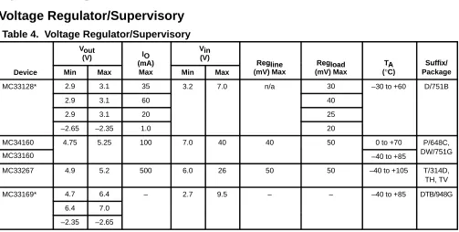
Special Regulators
[image:9.612.66.569.63.317.2]Voltage Regulator/Supervisory
Table 4. Voltage Regulator/Supervisory
D i
Vout
(V) IO
(mA)
Vin (V)
Regline Regload TA Suffix/ Device Min Max
(mA)
Max Min Max
Regline (mV) Max
Regload (mV) Max
TA (°C)
Suffix/ Package
MC33128* 2.9 3.1 35 3.2 7.0 n/a 30 –30 to +60 D/751B
2.9 3.1 60 40
2.9 3.1 20 25
–2.65 –2.35 1.0 20
MC34160 4.75 5.25 100 7.0 40 40 50 0 to +70 P/648C,
DW/751G
MC33160 –40 to +85 DW/751G
MC33267 4.9 5.2 500 6.0 26 50 50 –40 to +105 T/314D,
TH, TV
MC33169* 4.7 6.4 – 2.7 9.5 – – –40 to +85 DTB/948G
6.4 7.0
–2.35 –2.65
Voltage Regulator/Supervisory
(continued)
Microprocessor Voltage Regulator and Supervisory Circuit
MC34160P, DWTA = 0° to +70°C, Case 648C, 751G
MC33160P, DW
TA = –40° to +85°C, Case 648C, 751G
The MC34160 series is a voltage regulator and supervisory circuit contain-ing many of the necessary monitorcontain-ing functions required in microprocessor based systems. It is specifically designed for appliance and industrial applications offering the designer a cost effective solution with minimal external components. These integrated circuits feature a 5.0 V, 100 mA regulator with short circuit current limiting, pinned out 2.6 V bandgap reference, low voltage reset comparator, power warning comparator with program-mable hysteresis, and an uncommitted comparator ideally suited for microproces-sor line synchronization.
Additional features include a chip disable input for low standby current, and internal thermal shutdown for over temperature protection.
These devices are contained in a 16 pin dual–in–line heat tab plastic package for improved thermal conduction.
Low Dropout Regulator
MC33267T, TVTJ = –40° to +105°C, Case 314D, 314B The MC33267 is a positive fixed 5.0 V regulator that is specifically designed to maintain proper voltage regulation with an extremely low input–to–output voltage differential. This device is capable of supplying output currents in excess of 500 mA and contains internal current limiting and thermal shutdown protection. Also featured is an on–chip power–up reset circuit that is ideally suited for use in microprocessor based systems. Whenever the regulator output voltage is below nominal, the reset output is held low. A programmable time delay is initiated after the regulator has reached its nominal level and upon timeout, the reset output is released.
Due to the low dropout voltage specifications, the MC33267 is ideally suited for use in battery powered industrial and consumer equipment where an extension of useful battery life is desirable. This device is contained in an economical five lead TO–220 type package.
VCC
Chip Disable
Power Sense
Hysteresis Adjust
Noninverting Input
Inverting Input
14
15
9
10
2
1
Regulator Output
Reset
Power Warning Reference Output
Comparator Output
Gnd 4, 5,12, 13 2.6 V
Reference
0.01R 0.913R
R
IH
IH “On”/“Off”
6 8 16 7 11 Thermal
Shutdown
Input Output
1 5
Reference 1.25 V
Thermal
Over Current Detector
Ground 3
1.25 V Delay R
0.03 R 3.01
R 20 µA
3.8 V Reset
200
Reset 2
Delay 4 +
Voltage Regulator/Supervisory
(continued)
Very Low Dropout Regulator
L4949N, D
TJ = –40° to +125°C, Case 626, 751 The L4949 is a monolithic integrated 5.0 V voltage regulator with a very low dropout and additional functions such as power–on reset and input voltage sense.
It is designed for supplying the micro–computer controlled systems especially in automotive applications.
• Operating DC Supply Voltage Range 5.0 V to 28 V
• Transient Supply Voltage Up to 40 V
• Extremely Low Quiescent Current in Standby Mode
• High Precision Standby Output Voltage 5.0 V ±1%
• Output Current Capability Up to 100 mA
• Very Low Dropout Voltage Less Than 0.4 V
• Reset Circuit Sensing The Output Voltage
• Programmable Reset Pulse Delay With External Capacitor
• Voltage Sense Comparator
• Thermal Shutdown and Short Circuit Protections
Power Management Controller
MC33128DTA = –30° to +60°C, Case 751B
The MC33128 is a power management controller specifically designed for use in battery powered cellular telephone and pager applications. This device contains all of the active functions required to interface the user to the system electronics via a microprocessor. This integrated circuit consists of a low dropout voltage regulator with power–up reset for MPU power, two low dropout voltage regulators for independant powering of analog and digital circuitry, and a negative charge pump voltage regulator for full depletion of gallium arsenide MESFETs.
Also included are protective system shutdown features consisting of a battery latch that is activated upon battery insertion, low battery voltage shutdown, and a thermal over temperature detector. This device is available in a 16–pin narrow body surface mount plastic package.
“On”/“Off” Toggle
VCC VBB CPC
VBB Output Control Logic Low Battery Shutdown Thermal Protection Reference Charge Pump Negative Standby Regulator Standby Regulator 1 Standby Regulator 2 MPU Regulator MPU Power Up Reset Reference Output
Gnd 6 12
10 11
16 3 2 4
8 7 5 15 1 14 VDD R I O O Output 4 CPC Output 4 –2.5 V/1.0 mA
Output 1 3.0 V/30 mA Output 2 3.0 V/60 mA Output 3 3.0 V/20 mA
MPU + 13 9 Regulator 1.23 Vref 2.0 V 2.0 µA
Reset 1.23 V Sense Gnd Sense Output (So) Reset Sense Input (Si) Supply Voltage (VCC) VZ Output Voltage (Vout) CT
3 8 4
GaAs Power Amplifier Support IC
MC33169DTBTA = –40° to +85°C, Case 948G
The MC33169 is a support IC for GaAs Power Amplifier Enhanced FETs used in hand portable telephones such as GSM, PCN and DECT. This device provides negative voltages for full depletion of Enhanced MESFETs as well as a priority management system of drain switching, ensuring that the negative voltage is always present before turning “on” the Power Amplifier. Additional features include an idle mode input and a direct drive of the N–Channel drain switch transistor.
This product is available in two versions, – 2.5 and – 4.0 V. The – 4.0 V version is intended for supplying RF modules for GSM and DCS1800 applications, whereas the – 2.5 V version is dedicated for DECT and PHS systems.
• Negative Regulated Output for Full Depletion of GaAs MESFETs
• Drain Switch Priority Management Circuit
• CMOS Compatible Inputs
• Idle Mode Input (Standby Mode) for Very Low Current Consumption
• Output Signal Directly Drives N–Channel FET
• Low Startup and Operating Current
VBB Double C3
VCC + –
C1
– + C2
VBB Triple
C4 + –
Tx Power Control Input
Idle Mode Input
Gnd
Cp + –
VO Output (– 2.5 V or – 4.0 V)
Ci
Rf Cf +
–
+ RF
In
RF Out +
VBattery (2.7 to 7.0 V)
Gate Drive Output
Sense Input VBB
Generator (Voltage Tripler)
Priority Management
Negative Generator Charge
Pump
Power Amplifier Sense
MC33169
MMSF4N01HD
2 1 14
8
10
4 5 7 6 13 9 3 11
SCSI Regulator
Table 5. SCSI Regulator
D i
Vout (V)
Isink
Vin (V)
Regline Regload TJ Suffix/ Device Min Max
Isink
(mA) Min Max
Regline (%)
Regload (%)
TJ (°C)
Suffix/ Package
MC34268 2.81 2.89 800 3.9 20 0.3 0.5 150 D/751, DT
SCSI–2 Active Terminator Regulator
MC34268D, DTTJ = 0° to +125°C, Case 751, 369A
The MC34268 is a medium current, low dropout positive voltage regulator specifically designed for use in SCSI–2 active termination circuits. This device offers the circuit designer an economical solution for precision voltage regulation, while keeping power losses to a minimum. The regulator consists of a 1.0 V dropout composite PNP/NPN pass transistor, current limiting, and thermal limiting. These devices are packaged in the 8–pin SOP–8 and 3–pin DPAK surface mount power packages.
Applications include active SCSI–2 terminators and post regulation of switching power supplies.
• 2.85 V Output Voltage for SCSI–2 Active Termination
• 1.0 V Dropout
• Output Current in Excess of 800 mA
• Thermal Protection
• Short Circuit Protection
• Output Trimmed to 1.4% Tolerance
• No Minimum Load Required
• Space Saving DPAK and SOP–8 Surface Mount Power Packages
Input
Thermal
Limiting ControlCircuit
Current
Limit Output
Switching Regulator Control Circuits
These devices contain the primary building blocks which are required to implement a variety of switching power supplies. The product offerings fall into three major categories consisting of single–ended and double–ended controllers, plus single–ended ICs with on–chip power switch transistors. These circuits operate in voltage, current or resonant modes
[image:14.612.56.552.197.675.2]and are designed to drive many of the standard switching topologies. The single–ended configurations include buck, boost, flyback and forward converters. The double–ended devices control push–pull, half bridge and full bridge configurations.
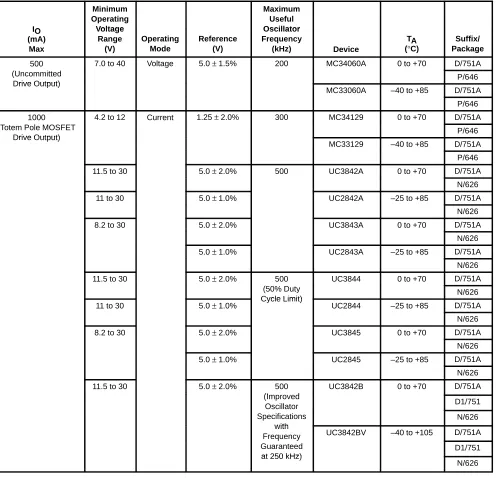
Table 6. Single–Ended Controllers
These single–ended voltage and current mode controllers are designed for use in buck, boost, flyback, and forward converters. They are cost effective in applications that range from 0.1 to 200 W power output.
IO
Minimum Operating Voltage
O i R f
Maximum Useful Oscillator
D i
T S ffi / IO
(mA) Max
Voltage Range
(V)
Operating Mode
Reference (V)
Oscillator Frequency
(kHz) Device
TA (°C)
Suffix/ Package
500
(U i d
7.0 to 40 Voltage 5.0 ± 1.5% 200 MC34060A 0 to +70 D/751A
(Uncommitted
Drive Output) P/646
Drive Output)
MC33060A –40 to +85 D/751A P/646 1000
(T t P l MOSFET
4.2 to 12 Current 1.25 ± 2.0% 300 MC34129 0 to +70 D/751A
(Totem Pole MOSFET
Drive Output) P/646
Drive Output)
MC33129 –40 to +85 D/751A P/646
11.5 to 30 5.0 ± 2.0% 500 UC3842A 0 to +70 D/751A
N/626
11 to 30 5.0 ±1.0% UC2842A –25 to +85 D/751A
N/626
8.2 to 30 5.0 ± 2.0% UC3843A 0 to +70 D/751A
N/626
5.0 ± 1.0% UC2843A –25 to +85 D/751A
N/626
11.5 to 30 5.0 ± 2.0% 500
(50% D
UC3844 0 to +70 D/751A
(50% Duty
Cycle Limit) N/626
11 to 30 5.0 ± 1.0% Cycle Limit) UC2844 –25 to +85 D/751A
N/626
8.2 to 30 5.0 ± 2.0% UC3845 0 to +70 D/751A
N/626
5.0 ± 1.0% UC2845 –25 to +85 D/751A
N/626
11.5 to 30 5.0 ± 2.0% 500
(Improved
UC3842B 0 to +70 D/751A
(Improved
Oscillator D1/751
Oscillator Specifications
with
N/626 with
Frequency UC3842BV –40 to +105 D/751A Frequency
Guaranteed at 250 kHz)
D1/751 at 250 kHz)
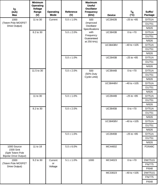
Table 6. Single–Ended Controllers (continued)
These single–ended voltage and current mode controllers are designed for use in buck, boost, flyback, and forward converters. They are cost effective in applications that range from 0.1 to 200 W power output.
IO (mA)
Max
Suffix/ Package TA
(°C) Device
Maximum Useful Oscillator Frequency
(kHz) Reference
(V) Operating
Mode Minimum
Operating Voltage
Range (V) IO
(mA) Max
Suffix/ Package TA
(°C) Device
Maximum Useful Oscillator Frequency
(kHz) Reference
(V) Operating
Mode Minimum
Operating Voltage
Range (V)
1000 (T t P l MOSFET
11 to 30 Current 5.0 ± 1.0% 500
(I d
UC2842B –25 to +85 D/751A (Totem Pole MOSFET
Drive Output)
(Improved
Oscillator D1/751
Drive Output) Oscillator
Specifications N/626
8.2 to 30 5.0 ± 2.0%
Specifications with F
UC3843B 0 to +70 D/751A
Frequency
Guaranteed D1/751
Guaranteed
at 250 kHz) N/626
at 250 kHz)
UC3843BV –40 to +105 D/751A D1/751 N/626
5.0 ± 1.0% UC2843B –25 to +85 D/751A
D1/751 N/626
11.5 to 30 5.0 ± 2.0% 500
(50% D
UC3844B 0 to +70 D/751A
(50% Duty
Cycle Limit) D1/751
Cycle Limit)
N/626 UC3844BV –40 to +105 D/751A
D1/751 N/626
11 to 30 5.0 ± 1.0% UC2844B –25 to +85 D/751A
D1/751 N/626
8.2 to 30 5.0 ± 2.0% UC3845B 0 to +70 D/751A
D1/751 N/626 UC3845BV –40 to +105 D/751A
D1/751 N/626
5.0 ± 1.0% UC2845B –25 to +85 D/751A
D1/751 N/626 1000 Source
1500 Sink (Split Totem Pole Bipolar Drive Output)
11 to 18 5.0 ± 6.0% MC44602 P2/648C
2000 (T P l MOSFET
9.2 to 30 Current 5.1 ± 1.0% 1000 MC34023 0 to +70 DW/751G
(Totem Pole MOSFET Drive Output)
or
Voltage FN/775
Drive Output) Voltage
P/648 MC33023 –40 to +105 DW/751G
Table 7. Single–Ended Controllers with On–Chip Power Switch
These monolithic power switching regulators contain all the active functions required to implement standard dc–to–dc These monolithic power switching regulators contain all the active functions required to implement standard dc–to–dc converter configurations with a minimum number of external components.
IO
Minimum Operating Voltage
O i R f
Maximum Useful Oscillator
D i
T S ffi / IO (mA) Max Voltage Range (V) Operating Mode Reference (V) Oscillator Frequency (kHz) Device TA (°C)
Suffix/ Package
1500 (U itt d
2.5 to 40 Voltage 1.25 ± 5.2%(1) 100 µA78S40 0 to +70 PC/648 (Uncommitted
Power Switch) –40 to +85 PV/648
Power Switch)
1.25 ± 2.0% MC34063A 0 to +70 D/751
P1/626 MC33063A –40 to +85 D/751
P1/626 –40 to +125 D/751 3400
(Uncommitted
2.5 to 40 Voltage 1.25 ± 2.0% and
100 MC34163 0 to +70 P/648C,
DW/751G (Uncommitted
Power Switch)
and
5.05 ± 3.0% MC33163 –40 to +85
DW/751G
3400(2) (Dedicated Emitter
7.5 to 40 5.05 ± 2.0% 72 ± 12% Internally
MC34166 0 to +70 D2T/936A, TH, TV, (Dedicated Emitter
Power Switch)
Internally
Fixed MC33166 –40 to +85
TH, TV, T/314D 5500(3)
(Dedicated Emitter
MC34167 0 to +70 (Dedicated Emitter
Power Switch) MC33167 –40 to +85
(1) Tolerance applies over the specified operating temperature range. (2) Guaranteed minimum, typically 4300 mA.
(3) Guaranteed minimum, typically 6500 mA.
Table 8. Easy Switcher
Single–Ended Controllers with On–Chip Power Switch
The Easy Switcher series is ideally suited for easy, convenient design of a step–down switching regulator (buck converter), with a minimum number of external components.
IO Minimum Operating Voltage O i Oscillator Output D i
T S ffi / IO (mA) Max Voltage Range (V) Operating Mode Oscillator Frequency (kHz) Output Voltage (V) Device TJ (°C)
Suffix/ Package
500 4.75 to 40 Voltage 52 Fixed 3.3 LM2574N–3.3 –40 to +125 N/626
500 4.75 to 40
8.0 to 40
Voltage 52 Fixed Internal
3.3 5.0
LM2574N 3.3 LM2574N–5
40 to +125 N/626 15 to 40
18 t 40
12 15
LM2574N–12 LM2574N 15 18 to 40
8 0 to 40
15 1 23 to 37
LM2574N–15 LM2574N ADJ
8.0 to 40 1.23 to 37 LM2574N–ADJ
1000 4.75 to 40 Voltage 52 Fixed 3.3 LM2575T–3.3 –40 to +125 T/314D
1000 4.75 to 40 8.0 to 40
Voltage 52 Fixed Internal
3.3 5.0
LM2575T 3.3 LM2575T–5
40 to +125 T/314D 15 to 40
18 t 40
12 15
LM2575T–12 LM2575T 15 18 to 40
8 0 to 40
15 1 23 to 37
LM2575T–15 LM2575T ADJ
8.0 to 40 1.23 to 37 LM2575T–ADJ
4.75 to 40 3.3 LM2575TV–3.3 TV/314B
4.75 to 40 8.0 to 40
3.3 5.0
LM2575TV 3.3 LM2575TV–5
TV/314B 15 to 40
18 t 40
12 15
LM2575TV–12 LM2575TV 15 18 to 40
8 0 to 40
15 1 23 to 37
LM2575TV–15 LM2575TV ADJ
8.0 to 40 1.23 to 37 LM2575TV–ADJ
4.75 to 40 3.3 LM2575D2T–3.3 D2T/936A
4.75 to 40 8.0 to 40
3.3 5.0
LM2575D2T 3.3 LM2575D2T–5
D2T/936A 15 to 40
18 t 40
12 15
LM2575D2T–12 LM2575D2T 15 18 to 40
8 0 to 40
15 1 23 to 37
LM2575D2T–15 LM2575D2T ADJ
[image:16.612.46.560.442.733.2]Table 8. Easy Switcher
Single–Ended Controllers with On–Chip Power Switch (continued)
The Easy Switcher series is ideally suited for easy, convenient design of a step–down switching regulator (buck converter), with a minimum number of external components.
IO (mA) Max Suffix/ Package TJ
(°C) Device Output Voltage (V) Oscillator Frequency (kHz) Operating Mode Minimum Operating Voltage Range (V) IO (mA) Max Suffix/ Package TJ
(°C) Device Output Voltage (V) Oscillator Frequency (kHz) Operating Mode Minimum Operating Voltage Range (V)
3000 4.75 to 40 Voltage 52 Fixed 3.3 LM2576T–3.3 –40 to +125 T/314D
3000 4.75 to 40 8.0 to 40
Voltage 52 Fixed Internal
3.3 5.0
LM2576T 3.3 LM2576T–5
40 to +125 T/314D 15 to 40
18 t 40
12 15
LM2576T–12 LM2576T 15 18 to 40
8 0 to 40
15 1 23 to 37
LM2576T–15 LM2576T ADJ
8.0 to 40 1.23 to 37 LM2576T–ADJ
4.75 to 40 3.3 LM2576TV–3.3 TV/314B
4.75 to 40 8.0 to 40
3.3 5.0
LM2576TV 3.3 LM2576TV–5
TV/314B 15 to 40
18 t 40
12 15
LM2576TV–12 LM2576TV 15 18 to 40
8 0 to 40
15 1 23 to 37
LM2576TV–15 LM2576TV ADJ
8.0 to 40 1.23 to 37 LM2576TV–ADJ
4.75 to 40 3.3 LM2576D2T–3.3 D2T/936A
4.75 to 40 8.0 to 40
3.3 5.0
LM2576D2T 3.3 LM2576D2T–5
D2T/936A 15 to 40
18 t 40
12 15
LM2576D2T–12 LM2576D2T 15 18 to 40
8 0 to 40
15 1 23 to 37
LM2576D2T–15 LM2576D2T ADJ
[image:17.612.68.571.368.474.2]8.0 to 40 1.23 to 37 LM2576D2T–ADJ
Table 9. Very High Voltage Single–Ended Controller with On–Chip Power Switch
This monolithic high voltage switching regulator is specifically designed to operate from a rectified ac line voltage source.g g g g p y g p g Included are an on–chip high voltage power switch, active off–line startup circuitry and a full featured PWM controller with fault protection.
Power Switch
Maximum Rating Startup
O i Feedback Maximum Useful Oscillator D i
T S ffi / VDS (V) IDS (mA)
Startup Input Max (V) Operating Mode Feedback Threshold (V) Oscillator Frequency (kHz) Device TJ (°C)
Suffix/ Package
500 2000 250 Voltage 2.6 ± 3.1% 1000 MC33362 –25 to +125 DW/751N,
P/648E
700 1000 450 MC33363 P/648E
700 1000 450 MC33363A
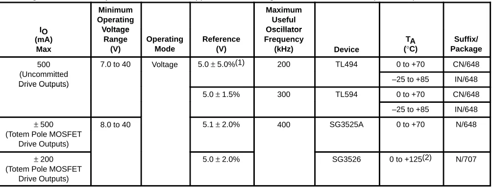
Table 10. Double–Ended Controllers
These double–ended voltage, current and resonant mode controllers are designed for use in push–pull, half–bridge, and full–bridge converters. They are cost effective in applications that range from 100 to 2000 watts power output.
IO
Minimum Operating Voltage
O i R f
Maximum Useful Oscillator
D i
T S ffi / IO (mA) Max Voltage Range (V) Operating Mode Reference (V) Oscillator Frequency (kHz) Device TA (°C)
Suffix/ Package
500 (U itt d
7.0 to 40 Voltage 5.0 ± 5.0%(1) 200 TL494 0 to +70 CN/648
(Uncommitted
Drive Outputs) –25 to +85 IN/648
Drive Outputs)
5.0 ± 1.5% 300 TL594 0 to +70 CN/648
–25 to +85 IN/648 ±500
(Totem Pole MOSFET Drive Outputs)
8.0 to 40 5.1 ± 2.0% 400 SG3525A 0 to +70 N/648
±200 (Totem Pole MOSFET
[image:17.612.67.569.531.723.2]Table 10. Double–Ended Controllers (continued)
These double–ended voltage, current and resonant mode controllers are designed for use in push–pull, half–bridge, and full–bridge converters. They are cost effective in applications that range from 100 to 2000 watts power output.
IO (mA)
Max
Suffix/ Package TA
(°C) Device
Maximum Useful Oscillator Frequency
(kHz) Reference
(V) Operating
Mode Minimum
Operating Voltage
Range (V) IO
(mA) Max
Suffix/ Package TA
(°C) Device
Maximum Useful Oscillator Frequency
(kHz) Reference
(V) Operating
Mode Minimum
Operating Voltage
Range (V)
±1500 (T t P l MOSFET
9.6 to 20 Resonant (Z
5.1 ± 2.0% 1000 MC34066 0 to +70 DW/751G
(Totem Pole MOSFET Drive Outputs)
(Zero
Current) P/648
Drive Outputs) Current)
MC33066 –40 to +85 DW/751G P/648 Resonant
(Z
2000 MC34067 0 to +70 DW/751G
(Zero
Voltage) P/648
Voltage)
MC33067 –40 to +85 DW/751G P/648 2000
(T t P l MOSFET
9.2 to 30 Current 5.1 ± 1.0% 1000 MC34025 0 to +70 DW/751G
(Totem Pole MOSFET Drive Outputs)
or
Voltage FN/775
Drive Outputs) Voltage
P/648 MC33025 –40 to +105 DW/751G
FN/775 P/648 (1) Tolerance applies over the specified operating temperature range.
Switching Regulator Control Circuits
(continued)CMOS Micropower DC–to–DC Converters
Variable Frequency Micropower DC–to–DC Converter
MC33463H
TA = –30° to +80°C, Case 1213
The MC33463 series are micropower step–up switching voltage regulators, specifically designed for handheld and laptop applications, to provide regulated output voltages using a minimum of external parts. A wide choice of output voltages are available. These devices feature a very low quiescent bias current of 4.0 µA typical.
The MC33463H–XXKT1 series features a highly accurate voltage reference, an oscillator, a variable frequency modula-tion (VFM) controller, a driver transistor (Lx), a comparator and feedback resistive divider.
T h e M C 3 3 4 6 3 H – X X LT 1 i s i d e n t i c a l t o t h e MC33463H–XXKT1, except that a drive pin (EXT) for an external transistor is provided.
Due to the low bias current specifications, these devices are ideally suited for battery powered computer, consumer,
and industrial equipment where an extension of useful bat-tery life is desirable.
MC33463 Series Features:
• Low Quiescent Bias Current of 4.0 µA
• High Output Voltage Accuracy of ±2.5%
• Low Startup Voltage of 0.9 V at 1.0 mA
• Wide Output Voltage Range of 2.5 V to 7.5 V Available
• High Efficiency of 80% Typical
• Surface Mount Package
ORDERING INFORMATION
Device
Output
Voltage Type
Operating Temperature Range
Package (Tape/Reel)
MC33463H–30KT1 3.0 Int.
S it h
T 30° 80°C
SOT–89 (T )
MC33463H–33KT1 3.3 Switch
T 30° 80°C
(Tape)
MC33463H–50KT1 5.0
TA = –30°to +80°C
MC33463H–30LT1 3.0 Ext.
S it h
TA = –30° to +80°C
SOT–89 (T )
MC33463H–33LT1 3.3 Switch
D i
(Tape)
MC33463H–50LT1 5.0 Drive
Other voltages from 2.5 V to 7.5 V, in 0.1 V increments are available. Consult factory for information.
MC33463H–XXKT1 MC33463H–XXLT1
XX Denotes Output Voltage Lx
D
Vin 3 VLx Limitier
Vref
Gnd VFM
Controller
100 kHz Oscillator
2 Output
VO
CO Drive
VFM Controller
100 kHz
Oscillator Vref D
Vin
Output VO
CO
Gnd 1 3
EXT L
Q Rb
Cb
1
2 Drive
L
Cin
CMOS Micropower DC–to–DC Converters
(continued)Fixed Frequency PWM Micropower DC–to–DC Converter
MC33466H
TA = –30° to +80°C, Case 1213
The MC33466 series are micropower switching voltage regulators, specifically designed for handheld and laptop applications, to provide regulated output voltages using a minimum of external parts. A wide choice of output voltages are available. These devices feature a very low quiescent bias current of 15 µA typical.
The MC33466H–XXJT1 series features a highly accurate voltage reference, an oscillator, a pulse width modulation (PWM) controller, a driver transistor (Lx), an error amplifier and feedback resistive divider.
T h e M C 3 3 4 6 6 H – X X LT 1 i s i d e n t i c a l t o t h e MC33466H–XXJT1, except that a drive pin (EXT) for an external transistor is provided.
Due to the low bias current specifications, these devices are ideally suited for battery powered computer, consumer, and industrial equipment where an extension of useful bat-tery life is desirable.
MC33466 Series Features:
• Low Quiescent Bias Current of 15 µA
• High Output Voltage Accuracy of ±2.5%
• Low Startup Voltage of 0.9 V at 1.0 mA
• Soft–Start = 500 µs
• Surface Mount Package
ORDERING INFORMATION
Device
Output
Voltage Type
Operating Temperature Range
Package (Tape/Reel)
MC33466H–30JT1 3.0 Int.
S it h
T 30° 80°C
SOT–89 (T )
MC33466H–33JT1 3.3 Switch
T 30° 80°C
(Tape)
MC33466H–50JT1 5.0
TA = –30°to +80°C
MC33466H–30LT1 3.0 Ext.
S it h
TA = –30° to +80°C
SOT–89 (T )
MC33466H–33LT1 3.3 Switch
D i
(Tape)
MC33466H–50LT1 5.0 Drive
Other voltages from 2.5 V to 7.5 V, in 0.1 V increments are available. Consult factory for information.
Gnd Drive
PWM Controller
50 kHz
Oscillator Vref
1
2 VO
MC33466H–XXJT1 MC33466H–XXLT1
Phase Comp
Soft–Start
Output (Voltage Feedback) 3
EXT
Gnd Drive
PWM Controller
50 kHz
Oscillator Vref
1
2 VO
Phase Comp
Soft–Start
Output (Voltage Feedback) 3
VLx Limiter Lx
Vin
Vin
XX Denotes Output Voltage CO
CO D
D L
L
Rb
Cb Q Cin
Switching Regulator Control Circuits
(continued)Synchronous Rectification DC/DC Converter
Programmable Integrated Controller
MC33470
TA = 0° to +75°C, Case 751D
The MC33470 is a digitally programmable switching volt-age regulator, specifically designed for Microprocessor sup-ply, Voltage Regulator Module and general purpose applica-tions, to provide a high power regulated output voltage using a minimum of external parts. A 5–bit digital–to–analog con-verter defines the dc output voltage.
This product has three additional features. The first is a pair of high speed comparators which monitor the output volt-age and expedite the circuit response to load current changes. The second feature is a soft start circuit which esta-blishes a controlled response when input power is applied and when recovering from external circuit fault conditions. The third feature is two output drivers which provide synchro-nous rectification for optimum efficiency.
This product is ideally suited for computer, consumer, and industrial equipment where accuracy, efficiency and optimum regulation performance is desirable.
MC33470 Features:
• 5–Bit Digital–to–Analog Converter Allows Digital Control of Output Voltage
• High Speed Response to Transient Load Conditions
• Output Enable Pin Provides On/Off Control
• Programmable Soft Start Control
• High Current Output Drives for Synchronous Rectification
• Internally Trimmed Reference with Low Temperature Coefficient
• Programmable Overcurrent Protection
• Overvoltage Fault Indication
• Functionally Similar to the LTC1553
ORDERING INFORMATION
Device
Operating
Temperature Range Package
Oscillator
PWM Comparator
OTA Error Amp
VCC
Sense
Compensation
PGnd G1
G2 Ifb Over Current
Detect Outen
Power Good
VID0 VID1 VID2 VID3
Vref
VCC
Voltage Identification
Code Input
Digitally Programmed Reference
VCC
Vref
R S
Q
PWM Latch +
0.96 Vref
1.04 Vref
5
VID4 18 17 16 15 14
4 10
9
14 3 1 8 20 2 19
0.93 Vref 1.04 Vref 13
AGnd 6 SS
800 µ
Over Temp
11
Imax 7
10 µA
2.5 V
1.5 V En
90 µA
190 µA
S R
Q
Delay Fault
1.14 Vref 20 µA
OT
Q
+
+
+
Delay
Simplified Block Diagram
Switching Regulator Control Circuits
(continued)Easy Switcher
Single–Ended Controllers with On–Chip Power Switch
Step–Down Voltage Regulators
LM2574N–XX
TJ = –40° to +125°C, Case 626
The LM2574 series of regulators are monolithic integrated circuits ideally suited for easy and convenient design of a step–down switching regulator (buck converter). All circuits of this series are capable of driving a 0.5 A load with excellent line and load regulation. These devices are available in fixed output voltages of 3.3 V, 5.0 V, 12 V, 15 V, and an adjustable output version.
These regulators were designed to minimize the number of external components to simplify the power supply design. Standard series of inductors optimized for use with the LM2574 are offered by several different inductor manufactur-ers.
Since the LM2574 converter is a switch–mode power sup-ply, its efficiency is significantly higher in comparison with popular three–terminal linear regulators, especially with high-er input voltages. In most cases, the powhigh-er dissipated by the LM2574 regulator is so low, that the copper traces on the printed circuit board are normally the only heatsink needed and no additional heatsinking is required.
The LM2574 features include a guaranteed ±4% tolerance on output voltage within specified input voltages and output load conditions, and ±10% on the oscillator frequency (±2% over 0°C to +125°C). External shutdown is included, featur-ing 60 µA (typical) standby current. The output switch in-cludes cycle–by–cycle current limiting, as well as thermal shutdown for full protection under fault conditions.
Features
• 3.3 V, 5.0 V, 12 V, 15 V, and Adjustable Output Versions
• Adjustable Version Output Voltage Range, 1.23 to 37 V
±4% max over Line and Load Conditions
• Guaranteed 0.5 A Output Current
• Wide Input Voltage Range: 4.75 to 40 V
• Requires Only 4 External Components
• 52 kHz Fixed Frequency Internal Oscillator
• TTL Shutdown Capability, Low Power Standby Mode
• High Efficiency
• Uses Readily Available Standard Inductors
• Thermal Shutdown and Current Limit Protection
Applications
• Simple and High–Efficiency Step–Down (Buck) Regulators
• Efficient Pre–Regulator for Linear Regulators
• On–Card Switching Regulators
• Positive to Negative Converters (Buck–Boost)
• Negative Step–Up Converters
• Power Supply for Battery Chargers
XX = Voltage Option, i.e., 3.3, 5, 12, 15 V; and ADJ for Adjustable Output
Representative Block Diagram and Typical Application
Unregulated DC Input
+Vin 5
Cout Feedback
1 Cin
L1
D1 R2
R1 1.0 k
Output 7 Pwr Gnd 4 ON/OFF 3
Reset Latch
Thermal Shutdown 52 kHz
Oscillator 1.235 V
Band–Gap Reference
Freq Shift 18 kHz
Comparator Fixed Gain
Error Amplifier
Current Limit
Driver
1.0 Amp Switch ON/OFF
3.1 V Internal Regulator
Vout
Load Output
Voltage Versions 3.3 V 5.0 V 12 V 15 V
R2 (Ω) 1.7 k 3.1 k 8.84 k 11.3 k For adjustable version R1 = open, R2 = 0 Ω
Step–Down Voltage Regulators
(continued)
LM2575T–XX, TV, D2T, LM2576T–XX, TV, D2T
TJ = –40° to +125°C, Case 314D, 314B, 936A
The LM2575/6 series of regulators are monolithic inte-grated circuits ideally suited for easy and convenient design of a step–down switching regulator (buck converter). All cir-cuits of this series are capable of driving a 1.0 A (LM2575) or
3.0 A (LM2576) load with excellent line and load regulation.
These devices are available in fixed output voltages of 3.3 V, 5.0 V, 12 V, 15 V, and an adjustable output version.
These regulators were designed to minimize the number of external components to simplify the power supply design. Standard series of inductors optimised for use with the LM2575/6 are offered by several different inductor manufac-turers.
Since the LM2575/6 converter is a switch–mode power supply, its efficiency is significantly higher in comparison with popular three–terminal linear regulators, especially with high-er input voltages. In many cases, the powhigh-er dissipated by the LM2575/6 regulator is so low, that no heatsink is required or its size could be reduced dramatically.
The LM2575/6 features include a guaranteed ±4% toler-ance on output voltage within specified input voltages and output load conditions, and ±10% on the oscillator frequency (±2% over 0°C to 125°C). External shutdown is included, fea-turing 80 µA typical standby current. The output switch in-cludes cycle–by–cycle current limiting, as well as thermal shutdown for full protection under fault conditions.
Features
• 3.3 V, 5.0 V, 12 V, 15 V, and Adjustable Output Versions
• Adjustable Version Output Voltage Range of 1.23 V to 37 V ±4% Maximum Over Line and Load Conditions
• Guaranteed 1.0 A (LM2575) 3.0 A (LM2576) Output Current
• Wide Input Voltage Range: 4.75 V to 40 V
• Requires Only 4 External Components
• 52 kHz Fixed Frequency Internal Oscillator
• TTL Shutdown Capability, Low Power Standby Mode
• High Efficiency
• Uses Readily Available Standard Inductors
• Thermal Shutdown and Current Limit Protection
Applications
• Simple and High–Efficiency Step–Down (Buck) Regulators
• Efficient Pre–Regulator for Linear Regulators
• On–Card Switching Regulators
• Positive to Negative Converters (Buck–Boost)
• Negative Step–Up Converters
• Power Supply for Battery Chargers
XX = Voltage Option, i.e., 3.3, 5, 12, 15 V; and ADJ for Adjustable Output
Representative Block Diagram and Typical Application
Unregulated DC Input
+Vin 1
Cout Feedback
4 Cin
L1
D1 R2
R1 1.0 k
Output 2 Gnd 3 ON/OFF 5
Reset Latch
Thermal Shutdown 52 kHz
Oscillator 1.235 V
Band–Gap Reference
Freq Shift 18 kHz
Comparator Fixed Gain
Error Amplifier
Current Limit
Driver
1.0 Amp Switch ON/OFF
3.1 V Internal Regulator
Regulated Output
Vout
Load Output
Voltage Versions 3.3 V 5.0 V 12 V 15 V
R2 (Ω) 1.7 k 3.1 k 8.84 k 11.3 k For adjustable version R1 = open, R2 = 0 Ω
Switching Regulator Control Circuits
(continued)Single–Ended GreenLine
Controllers
Enhanced Mixed Frequency Mode GreenLine
PWM Controller:
Fixed Frequency, Variable Frequency, Standby Mode
MC44603AP, DW
TA = –25° to +85°C, Case 648, 751G
The MC44603A is an enhanced high performance control-ler that is specifically designed for off–line and dc–to–dc con-verter applications. This device has the unique ability of auto-matically changing operating modes if the converter output is overloaded, unloaded, or shorted, offering the designer addi-tional protection for increased system reliability. The MC44603A has several distinguishing features when compared to conventional SMPS controllers. These features consist of a foldback facility for overload protection, a standby mode when the converter output is slightly loaded, a demagnetization detection for reduced switching stresses on transistor and diodes, and a high current totem pole output ideally suited for driving a power MOSFET. It can also be used for driving a bipolar transistor in low power converters (< 150 W). It is optimized to operate in discontinuous mode but can also operate in continuous mode. Its advanced design allows use in current mode or voltage mode control applications.
Current or Voltage Mode Controller
• Operation up to 250 kHz Output Switching Frequency
• Inherent Feed Forward Compensation
• Latching PWM for Cycle–by–Cycle Current Limiting
• Oscillator with Precise Frequency Control
High Flexibility
• Externally Programmable Reference Current
• Secondary or Primary Sensing
• Synchronization Facility
• High Current Totem Pole Output
• Undervoltage Lockout with Hysteresis
Safety/Protection Features
• Overvoltage Protection Against Open Current and Open Voltage Loop
• Protection Against Short Circuit on Oscillator Pin
• Fully Programmable Foldback
• Soft–Start Feature
• Accurate Maximum Duty Cycle Setting
• Demagnetization (Zero Current Detection) Protection
• Internally Trimmed Reference
• Enhanced Output Drive
GreenLine Controller: Low Power Consumption in Standby Mode
• Low Startup and Operating Current
• Fully Programmable Standby Mode
• Controlled Frequency Reduction in Standby Mode
• Low dV/dT for Low EMI Radiations
High Safety Standby Ladder Mode GreenLine
PWM Controller
MC44604P
TA = –25° to +85°C, Case 648
The MC44604 is an enhanced high performance controller that is specifically designed for off–line and dc–to–dc con-verter applications.
The MC44604 is a modification of the MC44603. The MC44604 offers enhanced safety and reliable power man-agement in its protection features (foldback, overvoltage detection, soft–start, accurate demagnetization detection). Its high current totem pole output is also ideally suited for driving a power MOSFET but can also be used for driving a bipolar transistor in low power converters (< 150 W).
In addition, the MC44604 offers a new efficient way to reduce the standby operating power by means of a patented standby ladder mode operation of the converter significantly reducing the converter consumption in standby mode.
Current or Voltage Mode Controller
• Operation Up to 250 kHz Output Switching Frequency
• Inherent Feed Forward Compensation
•
High Flexibility
• Externally Programmable Reference Current
• Secondary or Primary Sensing
• High Current Totem Pole Output
• Undervoltage Lockout with Hysteresis
Safety/Protection Features
• Overvoltage Protection Facility Against Open Loop
• Protection Against Short Circuit on Oscillator Pin
• Fully Programmable Foldback
• Soft–Start Feature
• Accurate Maximum Duty Cycle Setting
• Demagnetization (Zero Current Detection) Protection
• Internally Trimmed Reference
GreenLine Controller:
• Low Startup and Operating Current
Single–Ended GreenLine
Controllers
(continued)High Safety Latched Mode GreenLine
PWM Controller
for (Multi)Synchronized Applications
MC44605P
TA = –25° to +85°C, Case 648
The MC44605 is a high performance current mode con-troller that is specifically designed for off–line converters. The MC44605 has several distinguishing features that make it particularly suitable for multisynchronized monitor applica-tions.
The MC44605 synchronization arrangement enables operation from 16 kHz up to 130 kHz. This product was optimized to operate with universal ac mains voltage from 80 V to 280 V, and its high current totem pole output makes it ideally suited for driving a power MOSFET.
The MC44605 protections provide well controlled, safe power management. Safety enhancements detect four differ-ent fault conditions and provide protection through a disab-ling latch.
Current or Voltage Mode Controller
• Current Mode Operation Up to 250 kHz Output Switching Frequency
• Inherent Feed Forward Compensation
• Latching PWM for Cycle–by–Cycle Current Limiting
• Oscillator with Precise Frequency Control
• Externally Programmable Reference Current
• Secondary or Primary Sensing (Availability of Error Amplifier Output)
• Synchronization Facility
• High Current Totem Pole Output
• Undervoltage Lockout with Hysteresis
• Low Output dV/dT for Low EMI
• Low Startup and Operating Current
Safety/Protection Features • Soft–Start Feature
• Demagnetization (Zero Current Detection) Protection
• Overvoltage Protection Facility Against Open Loop
• EHT Overvoltage Protection (E.H.T.OVP): Protection Against Excessive Amplitude Synchronization Pulses
• Winding Short Circuit Detection (W.S.C.D.)
• Limitation of the Maximum Input Power (M.P.L.): Calculation of Input Power for Overload Protection
• Over Heating Detection (O.H.D.): to Prevent the Power Switch from Excessive Heating
Latched Disabling Mode
• When one of the following faults is detected: EHT overvoltage, Winding Short Circuit (WSCD), excessive input power (M.P.L.), power switch over heating (O.H.D.), a counter is activated
Switching Regulator Control Circuits
(continued)Very High Voltage Switching Regulator
MC33362DW, P
TJ = –25° to +125°C, Case 751N, 658E
The MC33362 is a monolithic high voltage switching regulator that is specifically designed to operate from a rectified 120 VAC line source. This integrated circuit features an on–chip 500 V/2.0 A SenseFET power switch, 250 V active off–line startup FET, duty cycle controlled oscillator, current limiting comparator with a programmable threshold and leading edge blanking, latching pulse width modulator for double pulse suppression, high gain error amplifier, and a trimmed internal bandgap reference. Protective features include cycle–by–cycle current limiting, input undervoltage lockout with hysteresis, output overvoltage protection, and
thermal shutdown. This device is available in a 16–lead dual–in–line and wide body surface mount packages.
• On–Chip 500 V, 2.0 A SenseFET Power Switch
• Rectified 120 VAC Line Source Operation
• On–Chip 250 V Active Off–Line Startup FET
• Latching PWM for Double Pulse Suppression
• Cycle–By–Cycle Current Limiting
• Input Undervoltage Lockout with Hysteresis
• Output Overvoltage Protection Comparator
• Trimmed Internal Bandgap Reference
• Internal Thermal Shutdown
20 W Off–Line Converter
Startup
Reg
Osc
Thermal
LEB PWM
DC Output Startup Input
Gnd 4, 5, 12, 13 Mirror
7 AC Input
Regulator Output
6 8
CT RT
PWM Latch
EA Ipk
VCC
3
11
16
9
10 1
Compensation
Voltage Feedback Input Power Switch Drain Overvoltage Protection Input
Driver
OVP UVLO
S
Switching Regulator Control Circuits
(continued)Very High Voltage Switching Regulator
MC33363DW, P, MC33363ADW, AP
TJ = –25° to +125°C, Case 751N, 648E
The MC33363 is a monolithic high voltage switching regu-lator that is specifically designed to operate from a rectified 240 Vac line source. This integrated circuit features an on– chip 700 V/1.0 A (1.5 A in MC33363A) SenseFET power switch, 450 V (500 V in MC33363A) active off–line startup FET, duty cycle controlled oscillator, current limiting comparator with a programmable threshold and leading edge blanking, latching pulse width modulator for double pulse suppression, high gain error amplifier, and a trimmed internal bandgap reference. Protective features include cycle–by– cycle current limiting, input undervoltage lockout with hyster-esis, output overvoltage protection, and thermal shutdown. This device is available in a 16–lead dual–in–line and wide body surface mount packages.
• On–Chip 700 V, 1.0 A SenseFET Power Switch
• On–Chip 700 V, 1.5 A SenseFET Power Switch in MC33363A
• Rectified 240 Vac Line Source Operation
• On–Chip 450 V Active Off–Line Startup FET
• On–Chip 500 V Active Off–Line Startup FET in MC33363A
• Latching PWM for Double Pulse Suppression
• Cycle–By–Cycle Current Limiting
• Input Undervoltage Lockout with Hysteresis
• Output Overvoltage Protection Comparator
• Trimmed Internal Bandgap Reference
• Internal Thermal Shutdown
Startup Reg
Osc
Thermal
LEB PWM
DC Output Startup Input
Gnd 4, 5, 12, 13 Mirror
7 AC Input
Regulator Output
6 8
CT RT
PWM Latch
EA Ipk
VCC 3
11 16
9
10 1
Compensation
Voltage Feedback Input Power Switch Drain Overvoltage Protection Input
Driver
OVP UVLO
S
Switching Regulator Control Circuits
(continued)High Voltage Switching Regulator
MC33363B
TJ = –25° to +125°C, Case 751G, 648E
The MC33363B is a monolithic high voltage switching reg-ulator that is specifically designed to operate from a rectified 240 Vac line source. This integrated circuit features an on–chip 700 V/1.0 A SenseFET power switch, 450 V active off–line startup FET, duty cycle controlled oscillator, current limiting comparator with a programmable threshold and lead-ing edge blanklead-ing, latchlead-ing pulse width modulator for double pulse suppression, high gain error amplifier, and a trimmed internal bandgap reference. Protective features include cycle–by–cycle current limiting, input undervoltage lockout with hysteresis, overvoltage protection, and thermal shut-down. This device is available in a 16–lead dual–in–line and wide body surface mount packages.
• On–Chip 700 V, 1.0 A SenseFET Power Switch
• Rectified 240 Vac Line Source Operation
• On–Chip 450 V Active Off–Line Startup FET
• Latching PWM for Double Pulse Suppression
• Cycle–By–Cycle Current Limiting
• Input Undervoltage Lockout with Hysteresis
• Output Overvoltage Protection
• Trimmed Internal Bandgap Reference
• Internal Thermal Shutdown
ORDERING INFORMATION
Device
Operating
Temperature Range Package
MC33363BDW
TJ = –25°to +125°C SOP–16L MC33363BP TJ = –25° to +125°C DIP–16
Simplified Application
Startup
Reg
Osc
Thermal
LEB PWM
DC Output Startup Input
Gnd 4, 5, 12, 13 Mirror
7 AC Input
Regulator Output
6 8
CT RT
PWM Latch
EA Ipk
VCC 3
11 16
9
10 1
Compensation
Voltage Feedback Input Power Switch Drain Overvoltage Protection Input
Driver OVP UVLO
S
Switching Regulator Control Circuits
(continued)Critical Conduction SMPS Controller
MC33364D, D1, D2
TJ = –25° to +125°C, Case 751, 751B
The MC33364 series are variable frequency SMPS control-lers that operate in the critical conduction mode. They are opti-mized for low power, high density power supplies requiring minimum board area, reduced component count, and low power dissipation. Each narrow body SOIC package provides a small footprint. Integration of the high voltage startup saves approximately 0.7 W of power compared to resistor boot-strapped circuits.
Each MC33364 features an on–board reference, UVLO function, a watchdog timer to initiate output switching, a zero current detector to ensure critical conduction operation, a current sensing comparator, leading edge blanking, and a CMOS driver. Protection features include the ability to shut down switchi