© 2019, IRJET | Impact Factor value: 7.211 | ISO 9001:2008 Certified Journal
| Page 1919
Energy Efficient one Bit Subtractor Circuits for Computing Applications
in Embedded Systems
S. Mohan Das
1, N. Ramanjaneyulu
21
Assistant Professor, S.V.R.Engineering College, Nandyal.
2P.G. Student, S.V.R.Engineering College, Nandyal.
---***---Abstract -As the technology goes down into the nano-scale domain, static or leakage power consumption becomes an important parameter in today’s VLSI design. In this paper, area-power-energy efficient 10 transistor 1-bit full subtractor has been proposed and compared with 20T and 14T one bit full subtractor circuits. The simulations for all the circuits were performed by using Microwind 3.1 CAD tool. Various parameters such as area, delay, power consumption PDP and EDP have been determined from Subtractor layout of feature size 45nm technology. The proposed 10 transistors full subtractor is energy efficient compared to other counterpart.
Key Words: Leakage power, Full subtractor, CAD tool.
1. INTRODUCTION
Low-power design techniques minimize active leakage power in nano scale CMOS VLSI systems. Developers of battery powered devices facing challenges to offer high levels of functionality, performance and simultaneously increasing life time of the battery. In some cases, battery developers are also challenged to develop next generation products with no battery at all, requiring energy harvesting from environmental sources such as light, heat and vibration[1] [2].
Leakage current and power is an important issue in Deep Sub Micron (DSM) technology. The main contribution of leakage power in CMOS circuits is due to dynamic power dissipation which increases with the reduction of channel length, threshold voltage and gate oxide thickness.
The total power dissipation of a logic gate is given by PTotal = PStatic + PDynamic + PShort Circuit
PTotal = IS VDD f + αCVDD2f + ISCVDDf
Where P switching is the power dissipated due to charging and discharging of the circuit capacitances, Pshort circuit is the power dissipated due to the short circuit between Vdd and ground during output transitions and Pleakage is the power dissipated due to leakage current. The term, Pleakage, is dramatically increased with technology down scaling and increase in temperature, resulting in a reduction of leakage [3] immunity and robustness. Among these Powers, short circuit power dissipation is very less i.e., almost negligible, when coming to static power dissipation it will occur only when gate is excited with inputs, which is also less compared to dynamic power dissipation as it occurs when transitions (charging and discharging) takes place
from high to low and vice –versa. More than 90 percent of power dissipation takes place due to dynamic activity of transistor switching in CMOS VLSI designs. Therefore, it is very vital to reduce the leakage power of dynamic logic gates.
Subtractor is a digital circuit that performs subtraction of numbers and which is one among the four basic binary operations. In most of the digital systems there is a requirement for calculating addresses, table indices frequently in some parts of processor which can be performed by a subtractor. Integration and differentiations are the two important mathematical operations which can be performed frequently in analog circuits where as in digital circuits, integration is similar to summation and differentiation is analogous to Subtraction. Unlike the addition operation, Subtraction in digital circuits may not be performed directly with logic gate because there is no direct subtraction logic with transistor. Subtraction in digital circuits performs by compliments [4] [5]. Full adders/subtractors are important components in applications such as digital signal processing (DSP) architectures and microprocessor. Microprocessors and digital signal processors rely on the efficient implementation of generic arithmetic logic units and floating-point units to execute dedicated algorithms.
2. LITERATURE REVIEW
M.Mahaboob Basha et.al. presented [4] the design of one bit full subtractor for energy efficient arithmetic application in signal processing applications. In this work, they focused on reducing the area of the digital circuit by reducing the transistor count. For all the proposed circuits the simulation has been carried out at 65 nm technology.
M.Mahaboob Basha et.al. proposed [5] low area high speed energy efficient one bit 10 transistors based full subtractor with MTCMOS for computing applications. In this work, they focused on reducing the lealage current whan the circuit is operated at less than 1 volts supply voltage. For all the proposed circuits the simulation has been carried out at 65 nm technology.
© 2019, IRJET | Impact Factor value: 7.211 | ISO 9001:2008 Certified Journal
| Page 1920
using CMOS 65nm technology with less number of transistors and hence it is efficient in area and reduces the complexity.
The design of Full subtractor has been obtained compared using auto generated layout, semi-custom layout and fully custom layout. Performing the simulation comparison is made between three layouts between auto generated, semicustom and fully custom on the basis of area. In this paper fully custom layout is 45% area efficient than auto generated and 41% than semicustom layout. Semi-custom is 6% area efficient than auto generated. Fully Semi-custom has better performance among the three layout techniques. From the above result analysis it is clear that the fully customized layout is more efficient in terms of area. Fully customized layout is 45% is better than semi-custom layout and 41% is better than auto generated layout approaches. So this design approach can be implemented where area reduction is the main consideration. In this approach power factor compensates for area.
Kamal Jeet Singh and Rajesh Mehra proposed [7] “Design &Analysis of Full Subtractor using 10T at 45nm Technology”. In this paper, a full subtractor is designed using XOR gate and GDI technique. The technology node used is 45nm. Transient analysis for XOR gate and GDI technique based full subtractor is performed. In analysis, we found that the full subtractor designed with XOR gate uses less number of transistor and consume less power than GDI technique based full subtractor. Full subtractor using XOR gate uses 10T where GDI based uses 14T. Power consumption and time delay is improved by 36.04% and 36.13% respectively when compared with GDI based full subtractor. It is found that XOR gate based full subtractor uses less number of transistors, less propagation delay and less power consumption when compared with GDI technique based full subtractor. XOR gate based full subtractor has power consumption of 1.81μW and delay time is 0.014ns whereas GDI technique based full subtractor have power consumption of 0.83μW and delay time is 0.023ns.
From the literature, in this work, an attempt is made to simulate the various one bit full subtractor at 45 nm technology by using Microwind 3.1 CAD tool. The proposed circuits could be an alternative in energy efficient divider applications [8].
3. PROPOSED DESIGN
Now a days, power consumption and sub threshold leakages are very challenging in the digital integrated circuit design. A scaling functionality and density of transistors are based on microprocessor chip. The scaling function helps to increase performance and operation speed of the integrated circuit design. In the present days, the leakage current and power are common problems in the digital circuit design. The digital system reliability can be improved by decreasing the physical size, weight, cost and which is accomplished by reducing the transistors count while designing the circuit.
Irjet Template sample paragraph .Define abbreviations and acronyms the first time they are used in the text, even after they have been defined in the abstract. Abbreviations such as IEEE, SI, MKS, CGS, sc, dc, and rms do not have to be defined. Do not use abbreviations in the title or heads unless they are unavoidable.
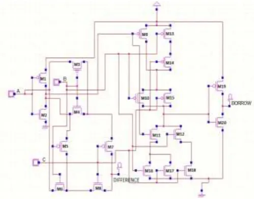
3.1. One Bit Full Subtractor By Using 20 Transistors
The circuit diagram of 1- bit full subtractor with 20 transistors is shown figure.1. The full subtractor design has less transistor count compared to the conventional full subtractor design. In this full subtractor design, 6 transistors employed for developing difference equation, 10 transistors used for borrow equation and remaining 4 transistors for inverting operation.
In this work, an attempt is made to design a one bit full subtractor with reduced transistor count from the massive literature of adder design. The circuit consist of 20 transistors which includes one 6 transistors EX-OR module, two CMOS inverters one at the difference output and other at the output of borrow and a section with 10 transistors which take care about the generation of borrow in correspond to the input bit variation and remaining modules.
The borrow section with ten transistors are made up with 5 PMOS and 5 NMOS transistors and this part is similar to that of carry section in a conventional 1-bit full adder. From the observation of the functional truth table of one bit adder and one bit subtractor it is clear that output sum of adder and difference output of subtractor are same whereas, they differs in output carry of adder in four outcomes among eight for one bit operation.
Fig -1: 20 transistors based 1-bit full subtractor
[image:2.595.310.560.499.694.2]© 2019, IRJET | Impact Factor value: 7.211 | ISO 9001:2008 Certified Journal
| Page 1921
voltage levels between the intermediate nodes as compared to conventional one at low supply voltages.
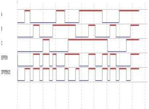
Fig -2: Timing waveform of 1-bit full subtractor using 20 transistors
3.2. One Bit Full Subtractor By Using 14 Transistors
The one bit full subtractor circuit consists of XOR-XNOR modules and a 2x1 multiplexer and requires 14 transistors to implement which is shown in figure.3. The XNOR - XOR modules produces two intermediate signals that are passed to 2×1 multiplexer. The two intermediate signals are provided by the above logic gates performances as input to 2×1 multiplexer and the third input performances as selection line used for multiplexer.
The difference output is obtained from 6T XOR-XNOR cell and a multiplexer, whereas borrow is obtained from 6T XOR gate. The 4T XOR module is employed by transistors M1, M2, M3 AND M4.
Fig -3: 14 transistors based 1-bit full subtractor
The timing waveform for the design circuit for different input combination is shown in below figure.4. With the involvement of multiplexer in the proposed design the circuit performance is better in comparison with 20T and C-CMOS one bit subtractor. Still the circuit suffers with sub threshold leakage current due to the feedback based 6T XOR gate when it operates with a supply voltage less than 1.8 volts.
Fig -4: Timing waveform of 1-bit full subtractor using 20 transistors
Figure.4. With the involvement of multiplexer in the proposed design the circuit performance is better in comparison with 20T and C-CMOS one bit subtractor. Still the circuit suffers with sub threshold leakage current due to the feedback based 6T XOR gate when it operates with a supply voltage less than 1.8 volts.
3.3. One Bit Full Subtractor By Using 10 Transistors
The figure.5 shows the logic circuit of one-bit full subtractor design using two XOR gates and one multiplexer which consists three inputs like A, B, and C and two outputs such as Difference and Borrow. The transistor level circuit is implemented by 4 transistor XOR gates and 2x1 multiplexer with two transistors. Furthermore, the difference outputs are obtained from second XOR gates and borrow from multiplexer.
[image:3.595.38.289.130.314.2] [image:3.595.310.559.185.337.2] [image:3.595.48.319.551.743.2] [image:3.595.63.551.571.738.2]© 2019, IRJET | Impact Factor value: 7.211 | ISO 9001:2008 Certified Journal
| Page 1922
The outcomes of the first XOR gate is considered as selection line employed for the multiplexer to pass the logic value. The B and C both act as inputs for the multiplexer.
Fig -6: (a) (b) Number of transistors used for the XOR gate and Multiplexer.
[image:4.595.42.284.148.268.2]The figure.6 (a) and (b) shows the transistor based circuits used for the XOR gate and multiplexer. The first EX-OR gate is employed with four transistors and other EX-EX-OR gate is employed with four transistors. The two transistors are the part of multiplexer. The proposed design was based on 10T one bit full adder with a bit of change in connections as well as selection of input combination to the multiplexer. Here the output of first XOR cell is select line for second XOR input and multiplexer. If first XOR output is at logic 0, the difference is same as input bit C only; otherwise the difference output is complement of input bit C. in case borrow output, if first EX-OR output is at logic 0, the borrow output is input bit C only. Similarly, if the first EX-OR gate output is at logic 1, the output borrow is input bit B only. Hence, the entire circuit operation for various possible input bit combination in terms of its timing waveform is depicted in figure 7.
Fig -7: Timing waveform of 1-bit full subtractor using 10 transistors
4. RESULTS, DISCUSSION AND CONCLUSION
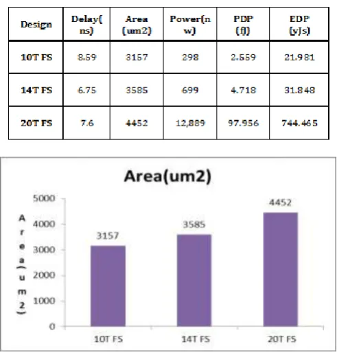
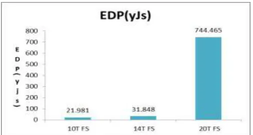
In this work various one-bit full subtractor circuits with reduced transistor count were analyzed and all the simulation has been carried out at 45nm technology with Microwind 3.1 CAD tool. From the simulations, the parameters like Area, Power, Delay, PDP and EDP were measured and compared with one-bit conventional full subtractor.
[image:4.595.311.557.275.537.2]Among 10T, 14T and 20T one bit full subtractor, the 10T one bit full subtractor is energy and EDP efficient which is shown in table 4.1.
Table 4.1
Fig -8: performance analysis of area for various 1-bit full subtractor circuits
[image:4.595.40.283.525.723.2] [image:4.595.309.557.562.701.2]© 2019, IRJET | Impact Factor value: 7.211 | ISO 9001:2008 Certified Journal
| Page 1923
Fig -10: performance analysis of power for various 1-bit full subtractor circuits
Fig -11: performance analysis of energy for various 1-bit full subtractor circuits
Fig -12: performance analysis of EDP for various 1-bit full subtractor circuits
The performance analysis of various one bit full subtractor circuits were shown in figure 8,9,10,11 and 12 in terms of area,delay,power,PDP and EDP respectively.
5. CONCLUSIONS
From the results it is clear that, the 10T one bit full subtractor occupies less area in comparison with other counter parts.
The power consumption of 10T one bit full subtractor is less in comparison with other counter parts whereas the delay of 10T one bit full subtractor is more when compared to 14T and 20T one bit full subtractor.
Therefore, the 10T one bit full subtractor is energy, EDP, power and area efficient at the cost of delay.
REFERENCES
[1] Neil Weste and D. Harris, “CMOS VLSI Design: A Circuit
and System Perspective,” Pearson Addition Wesley, third Edition, 2005.
[2] Ken Martin, Digital Integrated Circuit Design, Oxford
University Press, New York, 2000.
[3] CMOS Digital Integrated Circuits Analysis and Design
Third Edition2003, By Sung-Mo Kang, Yusuf Leblebici.
[4] M. Mahaboobbasha, K. Venkataramanaiah, P. Ramana
Reddy. “Noval energy efficient one bit full subtractor at 65nm technology”. International conference on electrical, electronics, signals, communication and optimization(EESCO), IEEE, Jan 2015.
[5] M. Mahaboobbasha, K. Venkataramanaiah, P. Ramana
Reddy, “low area high speed energy efficient one bit full subtractor with MTCMOS”. International Journal of Applied Engineering Research. Volume 10, Number 11 (2015) pp. 27593-27604.
[6] Anamika Sharma, Rajesh Mehra “Area Efficient Layout
Design & Analysis of Full Subtractor” IJSRET EATHD-2015 Conference Proceeding, 14-15 March, EATHD-2015.
[7] Kamal Jeet Singh, Rajesh Mehra “Design &Analysis of
Full Subtractor using 10T at 45nm Technology” IJETT, Volume 35 Number 9 - May 2016.
[8] M.Mahaboob Basha, Dr. K.Venkata Ramanaiah, Dr.
P.Ramana Reddy, Salendra. Govindarajulu.” Novel low Power and high speed array divider in 65nm technology” International Journal of Advances in Science and Technology Vol. 6, No. 6, 2013.
[9] B. K. Mohanty and P. K. Meher, "Area–Delay–Energy
Efficient VLSI Architecture for Scalable In-Place Computation of FFT on Real Data," in IEEE Transactions on Circuits and Systems I: Regular Papers, vol. 66, no. 3, pp. 1042-1050, March 2019.
[10] M.Mahaboob Basha, K.Venkata Ramanaiah, P. Ramana
[image:5.595.35.289.465.601.2]