Chapter 2
Parallel Computer Architecture
The possibility for a parallel execution of computations strongly depends on the architecture of the execution platform. This chapter gives an overview of the gen-eral structure of parallel computers which determines how computations of a pro-gram can be mapped to the available resources, such that a parallel execution is obtained. Section 2.1gives a short overview of the use of parallelism within a single processor or processor core. Using the available resources within a single processor core at instruction level can lead to a significant performance increase. Sections2.2 and2.3describe the control and data organization of parallel platforms. Based on this, Sect.2.4presents an overview of the architecture of multicore processors and describes the use of thread-based parallelism for simultaneous multithreading.
The following sections are devoted to specific components of parallel platforms. Section2.5describes important aspects of interconnection networks which are used to connect the resources of parallel platforms and which are used to exchange data and information between these resources. Interconnection networks also play an impor-tant role for multicore processors for the connection between the cores of a proces-sor chip. Section2.5describes static and dynamic interconnection networks and dis-cusses important characteristics like diameter, bisection bandwidth, and connectivity of different network types as well as the embedding of networks into other networks. Section2.6addresses routing techniques for selecting paths through networks and switching techniques for message forwarding over a given path. Section2.7 con-siders memory hierarchies of sequential and parallel platforms and discusses cache coherence and memory consistency for shared memory platforms. As example for the architecture of a large parallel system, Sect.2.8gives a short description of the IBM Blue Gene/Q series.
2.1 Processor Architecture and Technology Trends
Processor chips are the key components of computers. Considering the trends that can be observed for processor chips during the last years, estimations for future developments can be deduced.
T. Rauber and G. Rünger,Parallel Programming, 9
An important performance factor is the clock frequency of the processor, which determines the cycle time of the processor and therefore the time needed for the execution of an instruction. Between 1987 and 2003, an average annual increase of about 40% could be observed for desktop processors [94]. Since 2003, the clock fre-quency of desktop processors remains nearly unchanged and no significant increases can be expected in the near future [93, 122]. The reason for this development lies in the fact that an increase in clock frequency leads to an increase in power con-sumption, mainly due to leakage currents which are transformed into heat, which then requires a larger amount of cooling. Using current state-of-the-art cooling tech-nology, processors with a clock rate significantly above 3.3GHz cannot be cooled permanently without a large additional effort. Another important influence on the processor development is technical improvements in processor manufacturing.
Internally, processor chips consist of transistors. The number of transistors con-tained in a processor chip can be used as a rough estimate of its complexity and performance.Moore’s lawis an empirical observation which states that the num-ber of transistors of a typical processor chip doubles every 18 to 24 months. This observation has first been made by Gordon Moore in 1965 and is now valid for more than 40 years. The increasing number of transistors can be used for architectural improvements like additional functional units, more and larger caches, and more registers.
In 2012, a typical desktop processor chip contains 1–3 billions transistors. For example, an Intel Core i7 Sandy Bridge quad-core processor contains 995 million transistors, an Intel Core i7 Bridge-HE-4 quad-core processor contains 1.4 billion transistors, and an Intel Xeon Westmore-EX 10-core processor contains 2.6 billion transistors.
The increase of the number of transistors and the increase in clock speed has lead to a significant increase in the performance of computer systems. Processor perfor-mance can be measured by specific benchmark programs that have been selected from different application areas to get a representative performance measure of com-puter systems. Often, the SPEC benchmarks (System Performance and Evaluation Cooperative) are used to measure the integer and floating point performance of com-puter systems [102, 94, 183], seehttp://www.spec.org.Measurements with these benchmarks show that between 1986 and 2003, an average annual performance increase of about 50% could be reached for desktop processors [94]. It can be noted that the time period of this large performance increase corresponds to the time period in which the clock frequency could be significantly increased each year. Since 2003, the average annual performance increase of desktop processors is about 22%. This is still a significant increase which is reached, although the clock frequency nearly remained constant, showing that the annual increase in transistor count has been used for architectural improvements that lead to a reduction of the average time for executing an instruction.
In the following, we give a short overview of such architectural improvements. Four phases of microprocessor design trends can be observed [41] which are mainly driven by the internal use of parallelism:
2.1 Processor Architecture and Technology Trends 11
1. Parallelism at bit level: Up to about 1986, the word size used by the processors for operations increased stepwise from 4 to 32 bits. This trend has slowed down and ended with the adoption of 64-bit operations beginning in the 1990s. This development has been driven by demands for improved floating point accuracy and a larger address space. The trend has stopped at a word size of 64 bits, since this gives sufficient accuracy for floating point numbers and covers a sufficiently large address space of 264bytes.
2. Parallelism by pipelining: The idea of pipelining at instruction level is an over-lapping of the execution of multiple instructions. The execution of each instruc-tion is partiinstruc-tioned into several steps which are performed by dedicated hardware units (pipeline stages) one after another. A typical partitioning could result in the following steps:
(a) fetch: fetch the next instruction to be executed from memory; (b) decode: decode the instruction fetched in step (a);
(c) execute: load the operands specified and execute the instruction; (d) write back: write the result into the target register.
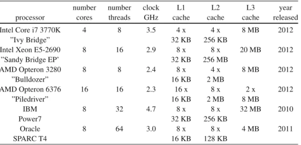
An instruction pipeline is like an assembly line in automobile industry. The advantage is that the different pipeline stages can operate in parallel, if there are no control or data dependencies between the instructions to be executed, see Fig.2.1for an illustration. To avoid waiting times, the execution of the different pipeline stages should take about the same amount of time. This time determines the cycle time of the processor. If there are no dependencies between the instructions, in each clock cycle the execution of one instruction is finished and the execution of another instruction is started. The number of instructions finished per time unit is defined as thethroughputof the pipeline. Thus, in the absence of dependencies, the throughput is one instruction per clock cycle. In the absence of dependencies, all pipeline stages work in parallel. Thus, the number of pipeline stages determines thedegree of parallelismattainable by a pipelined computation. The number of pipeline stages used in practice depends on the specific instruction and its potential to be partitioned into stages. Typical numbers of pipeline stages lie between 2 and 26 stages. Processors which use pipelining to execute instructions are calledILP processors (instruction level parallelism). Processors with a relatively large number of pipeline stages are sometimes calledsuperpipelined. Although the available degree of parallelism
Fig. 2.1 Overlapping exe-cution of four independent instructions by pipelining. The execution of each instruc-tion is split into four stages:
fetch(F),decode(D),execute
(E), andwrite back(W).
F2 F3 F4 D1 D2 D3 D4 E1 E2 E3 E4 W1 W2 W4 1 t t2 t3 t4 F1 W3 instruction 4 instruction 3 instruction 2 instruction 1 time
increases with the number of pipeline stages, this number cannot be arbitrarily increased, since it is not possible to partition the execution of the instruction into a very large number of steps of equal size. Moreover, data dependencies often inhibit a completely parallel use of the stages.
3. Parallelism by multiple functional units: Many processors aremultiple-issue processors. They use multiple, independent functional units like ALUs ( arith-metic logical unit), FPUs (floating point unit), load/store units, or branch units. These units can work in parallel, i.e., different independent instructions can be executed in parallel by different functional units. Thus, the average execution rate of instructions can be increased. Multiple-issue processors can be distin-guished intosuperscalarprocessors andVLIW(very long instruction word) processors, see [94, 41] for a more detailed treatment.
The number of functional units that can efficiently be utilized is restricted because of data dependencies between neighboring instructions. For superscalar proces-sors, these dependencies are determined at runtime dynamically by the hard-ware, and decoded instructions are dispatched to the instruction units using dynamic scheduling by the hardware. This may increase the complexity of the circuit significantly. Moreover, simulations have shown that superscalar proces-sors with up to four functional units yield a substantial benefit over a single func-tional unit. But using even more funcfunc-tional units provides little addifunc-tional gain [41, 110] because of dependencies between instructions and branching of control flow.
4. Parallelism at process or thread level: The three techniques described so far assume asingle sequentialcontrol flow which is provided by the compiler and which determines the execution order if there are dependencies between instruc-tions. For the programmer, this has the advantage that a sequential programming language can be used nevertheless leading to a parallel execution of instructions. However, the degree of parallelism obtained by pipelining and multiple func-tional units is limited. This limit has already been reached for some time for typical processors. But more and more transistors are available per processor chip according to Moore’s law. This can be used to integrate larger caches on the chip. But the cache sizes cannot be arbitrarily increased either, as larger caches lead to a larger access time, see Section2.7.
An alternative approach to use the increasing number of transistors on a chip is to put multiple, independent processor cores onto a single processor chip. This approach has been used for typical desktop processors since 2005. The resulting processor chips are calledmulticore processors. Each of the cores of a multicore processor must obtain a separate flow of control, i.e., parallel programming techniques must be used. The cores of a processor chip access the same memory and may even share caches. Therefore, memory accesses of the cores must be coordinated. The coordination and synchronization techniques required are described in later chapters.
2.1 Processor Architecture and Technology Trends 13
A more detailed description of parallelism by multiple functional units can be found in [41, 94, 155, 184]. Section2.4describes techniques like simultaneous multithreading and multicore processors requiring an explicit specification of parallelism.
2.2 Flynn’s Taxonomy of Parallel Architectures
Parallel computers have been used for many years, and many different architec-tural alternatives have been proposed and used. In general, a parallel computer can be characterized as a collection of processing elements that can communicate and cooperate to solve large problems fast [14]. This definition is intensionally quite vague to capture a large variety of parallel platforms. Many important details are not addressed by the definition, including the number and complexity of the process-ing elements, the structure of the interconnection network between the processprocess-ing elements, the coordination of the work between the processing elements as well as important characteristics of the problem to be solved.
For a more detailed investigation, it is useful to make a classification according to important characteristics of a parallel computer. A simple model for such a clas-sification is given byFlynn’s taxonomy[58]. This taxonomy characterizes parallel computers according to the global control and the resulting data and control flows. Four categories are distinguished:
1. Single Instruction, Single Data (SISD): There is one processing element which has access to a single program and data storage. In each step, the processing ele-ment loads an instruction and the corresponding data and executes the instruc-tion. The result is stored back in the data storage. Thus, SISD is the conventional sequential computer according to thevon Neumann model.
2. Multiple Instruction, Single Data (MISD): There are multiple processing ele-ments each of which has a private program memory, but there is only one common access to a single global data memory. In each step, each processing element obtains thesamedata element from the data memory and loads an instruction from its private program memory. These possibly different instructions are then executed in parallel by the processing elements using the previously obtained (identical) data element as operand. This execution model is very restrictive and no commercial parallel computer of this type has ever been built.
3. Single Instruction, Multiple Data (SIMD): There are multiple processing ele-ments each of which has a private access to a (shared or distributed) data memory, see Section2.3for a discussion of shared and distributed address spaces. But there is only one program memory from which a special control processor fetches and dispatches instructions. In each step, each processing element obtains from the control processor and thesameinstruction and loads a separate data element through its private data access on which the instruction is performed. Thus, the instruction is synchronously applied in parallel by all processing elements to different data elements.
For applications with a significant degree of data parallelism, the SIMD approach can be very efficient. Examples are multimedia applications or computer graphics algorithms to generate realistic three-dimensional views of computer-generated environments.
4. Multiple Instruction, Multiple Data (MIMD): There are multiple processing elements each of which has a separate instruction and data access to a (shared or distributed) program and data memory. In each step, each processing element loads a separate instruction and a separate data element, applies the instruction to the data element, and stores a possible result back into the data storage. The processing elements work asynchronously to each other. Multicore processors or cluster systems are examples for the MIMD model.
Compared to MIMD computers, SIMD computers have the advantage that they are easy to program, since there is only one program flow, and the synchronous execution does not require synchronization at program level. But the synchronous execution is also a restriction, since conditional statements of the form
if (b==0) c=a; else c = a/b;
must be executed in two steps. In the first step, all processing elements whose local value ofbis zero execute thethenpart. In the second step, all other processing elements execute theelsepart.
Some processors support SIMD computations as additional possibility for process-ing large uniform data sets. An example is the x86 architecture which provides SIMD instructions in the form of SSE (streaming SIMD extensions) or AVX (advanced vector extensions) instructions, see Sect.3.4for a more detailed description. The computations of GPUs are also based on the SIMD concept, see Sect.7.1.
MIMD computers are more flexible as SIMD computers, since each processing element can execute its own program flow. On the upper level, multicore processors as well as all parallel computers are based on the MIMD concept. Although Flynn’s taxonomy only provides a coarse classification, it is useful to give an overview of the design space of parallel computers.
2.3 Memory Organization of Parallel Computers
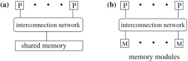
Nearly, all general-purpose parallel computers are based on the MIMD model. A fur-ther classification of MIMD computers can be done according to their memory orga-nization. Two aspects can be distinguished: the physical memory organization and the view of the programmer of the memory. For the physical organization, computers with a physically shared memory (also calledmultiprocessors) and computers with a physically distributed memory (also calledmulticomputers) can be distinguished, see Fig.2.2for an illustration. But there exist also many hybrid organizations, for example providing a virtually shared memory on top of a physically distributed memory.
2.3 Memory Organization of Parallel Computers 15 computers with memory shared computers with distributed memory
MIMD computer systems
Multicomputer systems shared computers with virtually memory
parallel and distributed
Multiprocessor systems
Fig. 2.2 Forms of memory organization of MIMD computers.
From the programmer’s point of view, it can be distinguished between computers with a distributed address space and computers with a shared address space. This view does not necessarily need to be conform with the physical memory. For exam-ple, a parallel computer with a physically distributed memory may appear to the programmer as a computer with a shared address space when a corresponding pro-gramming environment is used. In the following, we have a closer look at the physical organization of the memory.
2.3.1 Co
m
p
u
te
r
s w
i
th D
i
st
ri
b
u
ted Me
m
o
ry
O
r
gan
i
zat
i
on
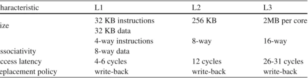
Computers with a physically distributed memory are also calleddistributed memory machines(DMM). They consist of a number of processing elements (called nodes) and an interconnection network which connects nodes and supports the transfer of data between nodes. A node is an independent unit, consisting of processor, local memory and, sometimes, periphery elements, see Fig.2.3a) for an illustration.
Program data are stored in the local memory of one or several nodes. All local memory isprivateand only the local processor can access the local memory directly. When a processor needs data from the local memory of other nodes to perform local computations, message passing has to be performed via the interconnection network. Therefore, distributed memory machines are strongly connected with the message-passing programming model which is based on communication between cooperat-ing sequential processes and which will be considered in more detail in Chapts.3 and5. To perform message passing, two processesPAandPBon different nodesA
andBissue corresponding send and receive operations. When PB needs data from
the local memory of node A, PAperforms a send operation containing the data for
the destination process PB. PB performs a receive operation specifying a receive
buffer to store the data from the source processPAfrom which the data are expected.
The architecture of computers with a distributed memory has experienced many changes over the years, especially concerning the interconnection network and the coupling of network and nodes. The interconnection network of earlier multicom-puters was often based onpoint-to-point connectionsbetween nodes. A node is
M P
DMA
R R R
R R R
R R R
computer with distributed memory
interconnection network with a hypercube as (a) (b) P M
(c) DMA (direct memory access)
(d) P M (e) R = Router M P DMA Router ... ... ... ... P M M P P M N N N N N N N N N interconnection network interconnection network = processor =local memory
node consisting of processor and local memory
with DMA connections to the network
external
input channels externaloutput channels
N = node consisting of processor and local memory
Fig. 2.3 Illustration of computers with distributed memory: (a) abstract structure, (b) computer with distributed memory and hypercube as interconnection structure, (c) DMA (direct memory access), (d) processor-memory node with router, and (e) interconnection network in form of a mesh to connect the routers of the different processor-memory nodes.
connected to a fixed set of other nodes by physical connections. The structure of the interconnection network can be represented as a graph structure. The nodes repre-sent the processors, the edges reprerepre-sent the physical interconnections (also called
2.3 Memory Organization of Parallel Computers 17
is the hypercubewhich is used in Fig.2.3b) to illustrate the node connections; a detailed description of interconnection structures is given in Sect.2.5. In networks with point-to-point connection, the structure of the network determines the possible communications, since each node can only exchange data with its direct neighbor. To decouple send and receive operations, buffers can be used to store a message until the communication partner is ready. Point-to-point connections restrict parallel pro-gramming, since the network topology determines the possibilities for data exchange, and parallel algorithms have to be formulated, such that their communication fits to the given network structure [8, 130].
The execution of communication operations can be decoupled from the proces-sor’s operations by adding aDMA controller(DMA - direct memory access) to the nodes to control the data transfer between the local memory and the I/O controller. This enables data transfer from or to the local memory without participation of the processor (see Fig.2.3c) for an illustration) and allows asynchronous communica-tion. A processor can issue a send operation to the DMA controller and can then continue local operations while the DMA controller executes the send operation. Messages are received at the destination node by its DMA controller which copies the enclosed data to a specific system location in local memory. When the processor then performs a receive operation, the data are copied from the system location to the specified receive buffer. Communication is still restricted to neighboring nodes in the network. Communication between nodes that do not have a direct connection must be controlled by software to send a message along a path of direct interconnections. Therefore, communication times between nodes that are not directly connected can be much larger than communication times between direct neighbors. Thus, it is still more efficient to use algorithms with communication according to the given network structure.
A further decoupling can be obtained by putting routers into the network, see Fig.2.3d). The routers form the actual network over which communication can be performed. The nodes are connected to the routers, see Fig.2.3e). Hardware-supported routing reduces communication times as messages for processors on remote nodes can be forwarded by the routers along a preselected path without interaction of the processors in the nodes along the path. With router support there is not a large difference in communication time between neighboring nodes and remote nodes, depending on the switching technique, see Sect.2.6.3. Each physical I/O channel of a router can be used by one message only at a specific point in time. To decouple message forwarding, message buffers are used for each I/O channel to store messages and apply specific routing algorithms to avoid deadlocks, see also Sect.2.6.1.
Technically, DMMs are quite easy to assemble since standard desktop computers can be used as nodes. The programming of DMMs requires a careful data layout, since each processor can directly access only its local data. Nonlocal data must be accessed via message passing, and the execution of the corresponding send and receive operations takes significantly longer than a local memory access. Depending on the interconnection network and the communication library used, the difference can be more than a factor of 100. Therefore, data layout may have a significant
influence on the resulting parallel runtime of a program. The data layout should be selected, such that the number of message transfers and the size of the data blocks exchanged are minimized.
The structure of DMMs has many similarities with networks of workstations (NOWs) in which standard workstations are connected by a fast local area network (LAN). An important difference is that interconnection networks of DMMs are typ-ically more specialized and provide larger bandwidths and lower latencies, thus leading to a faster message exchange.
Collections of complete computers with a dedicated interconnection network are often calledclusters. Clusters are usually based on standard computers and even standard network topologies. The entire cluster is addressed and programmed as a single unit. The popularity of clusters as parallel machines comes from the availability of standard high-speed interconnections like FCS (Fibre Channel Standard), SCI (Scalable Coherent Interface), Switched Gigabit Ethernet, Myrinet, or InfiniBand, see [158, 94, 155]. A natural programming model of DMMs is the message-passing model that is supported by communication libraries like MPI or PVM, see Chapt.5 for a detailed treatment of MPI. These libraries are often based on standard protocols like TCP/IP [125, 157].
The difference between cluster systems anddistributed systemslies in the fact that the nodes in cluster systems use the same operating system and can usually not be addressed individually; instead a special job scheduler must be used. Several cluster systems can be connected to grid systemsby using middleware software, such as the Globus Toolkit, seehttp://www.globus.org [65]. This allows a coordinated collaboration of several clusters. In grid systems, the execution of application programs is controlled by the middleware software.
Cluster systems are also used for the provision of services in the area of cloud computing. Using cloud computing, each user can allocate virtual resources which are provided via the cloud infrastructure as part of the cluster system. The user can dynamically allocate resources according to his or her computational requirements. Depending on the allocation, a virtual resource can be a single cluster node or a collection of cluster nodes. Examples for cloud infrastructures are the Amazon Elastic Compute Cloud (EC2) or the Windows Azure platform.
2.3.2 Co
m
p
u
te
r
s w
i
th Sha
r
ed Me
m
o
ry
O
r
gan
i
zat
i
on
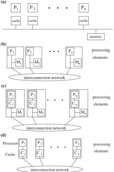
Computers with a physically shared memory are also called shared memory machines (SMMs); the shared memory is also called global memory. SMMs consist of a number of processors or cores, a shared physical memory (global memory) and an interconnection network to connect the processors with the memory. The shared memory can be implemented as a set of memory modules. Data can be exchanged between processors via the global memory by reading or writing shared variables. The cores of a multicore processor are an example for an SMM, see Sect.2.4.3for a more detailed description. Physically, the global memory usually consists of separate
2.3 Memory Organization of Parallel Computers 19
memory modules providing a common address space which can be accessed by all processors, see Fig.2.4for an illustration.
A natural programming model for SMMs is the use ofshared variableswhich can be accessed by all processors. Communication and cooperation between the processors is organized by writing and reading shared variables that are stored in the global memory. Accessing shared variables concurrently by several processors should be avoided sincerace conditionswith unpredictable effects can occur, see also Chaps.3and6.
The existence of a global memory is a significant advantage, since communica-tion via shared variables is easy and since no data replicacommunica-tion is necessary as it is sometimes the case for DMMs. But technically, the realization of SMMs requires a larger effort, in particular because the interconnection network must provide fast access to the global memory for each processor. This can be ensured for a small number of processors, but scaling beyond a few dozen processors is difficult.
A special variant of SMMs are symmetric multiprocessors (SMPs). SMPs have a single shared memory which provides a uniform access time from any processor for all memory locations, i.e., all memory locations are equidistant to all processors [41, 94]. SMPs usually have a small number of processors that are connected via a central bus which also provides access to the shared memory. There are usually no private memories of processors or specific I/O processors, but each processor has a private cache hierarchy. As usual, access to a local cache is faster than access to the global memory. In the spirit of the definition from above, each multicore processor with several cores is an SMP system.
SMPs usually have only a small number of processors, since the central bus provides a constant bandwidth which is shared by all processors. When too many processors are connected, more and more access collisions may occur, thus increas-ing the effective memory access time. This can be alleviated by the use of caches and suitable cache coherence protocols, see Sect.2.7.3. The maximum number of processors used in bus-based SMPs typically lies between 32 and 64.
Parallel programs for SMMs are often based on the execution of threads. A thread is a separate control flow which shares data with other threads via a global address space. It can be distinguished betweenkernel threadsthat are managed by the oper-ating system, anduser threadsthat are explicitly generated and controlled by the
M M
P P P P
interconnection network interconnection network
memory modules shared memory
(a) (b)
Fig. 2.4 Illustration of a computer with shared memory: (a) abstract view and (b) implementation of the shared memory with memory modules.
parallel program, see Section3.8.2. The kernel threads are mapped by the operating system to processors for execution. User threads are managed by the specific pro-gramming environment used and are mapped to kernel threads for execution. The mapping algorithms as well as the exact number of processors can be hidden from the user by the operating system. The processors are completely controlled by the operating system. The operating system can also start multiple sequential programs from several users on different processors, when no parallel program is available. Small size SMP systems are often used as servers, because of their cost-effectiveness, see [41, 158] for a detailed description.
SMP systems can be used as nodes of a larger parallel computer by employing an interconnection network for data exchange between processors of different SMP nodes. For such systems, a shared address space can be defined by using a suitable cache coherence protocol, see Sect.2.7.3. A coherence protocol provides the view of a shared address space, although the physical memory might be distributed. Such a protocol must ensure that any memory access returns the most recently written value for a specific memory address, no matter where this value is physically stored. The resulting systems are also called distributed shared memory (DSM) architectures. In contrast to single SMP systems, the access time in DSM systems depends on the location of a data value in the global memory, since an access to a data value in the local SMP memory is faster than an access to a data value in the memory of another SMP node via the coherence protocol. These systems are therefore also called NUMAs (nonuniform memory access), see Fig.2.5. Since single SMP systems have a uniform memory latency for all processors, they are also called UMAs (uniform memory access).
2.3.3 Red
u
c
i
ng
m
e
m
o
ry
access t
im
es
Memory access time has a large influence on program performance. This can also be observed for computer systems with a shared address space. The technologi-cal development with a steady reduction in the VLSI (Very-large-stechnologi-cale integration) feature size has led to significant improvements in processor performance. Since 1980, integer and floating-point performance on the SPEC benchmark suite has been increasing substantially per year, see Sect.2.1. A significant contribution to these improvements comes from a reduction in processor cycle time. At the same time, the capacity of DRAM chips, which are used for building main memory, increased significantly: Between 1986 and 2003, the capacity of DRAM chips increased by about 60% per year; since 2003, the annual average increase lies between 25% and 40% [94].
For a performance evaluation of DRAM chips, thelatencyand thebandwidth, also denoted as throughput, are used. The latency of a DRAM chip is the total time that elapses until a memory access operation has been completely terminated. The latency is typically measured in microseconds or nanoseconds. The bandwidth denotes the number of data elements that can be read from a DRAM chip per time unit.
2.3 Memory Organization of Parallel Computers 21
P
1P
2P
n(a)
cache cache cache
memory P1 P2 Pn M1 M2 Mn (b) interconnection network processing elements interconnection network 1 P P2 Pn 1 C C2 Cn M M M1 2 n (c) processing elements 1 n 1 2 n 2 P P P C C C Cache (d) Prozessor interconnection network processing elements
Fig. 2.5 Illustration of the architecture of computers with shared memory:(a)SMP – symmetric multiprocessors,(b)NUMA – nonuniform memory access,(c)CC-NUMA – cache coherent NUMA and(d)COMA – cache only memory access.
The bandwidth is typically measured in megabytes per second (MB/s) or gigabytes per second (GB/s). For the latency of DRAM chips, an average decrease of about 5% per year can be observed since 1980 [94]. In 2012, the latency of the newest DRAM technology (DDR3,Double Data Rate) lies between 24 and 30 ns. For the bandwidth of DRAM chips, an average increase of about 10% can be observed. For the DDR4 technology, which will be available in 2014, a bandwidth between 2100 MB/s and 3200 MB/s per DRAM chip is expected. Several DRAM chips (typically between 4
and 16) can be connected to DIMMs (dual inline memory module) to provide even larger bandwidths.
Considering DRAM latency, it can be observed that memory access time does not keep pace with processor performance improvement, and there is an increasing gap between processor cycle time and memory access time. A suitable organization of memory access becomes more and more important to get good performance results at program level. This is also true for parallel programs, in particular if a shared address space is used. Reducing the average latency observed by a processor when accessing memory can increase the resulting program performance significantly.
Two important approaches have been considered to reduce the average latency for memory access [14]: the simulation ofvirtual processorsby each physical processor (multithreading) and the use oflocal cachesto store data values that are accessed often. We give now a short overview of these approaches in the following.
2.3.3.1 Multithreading
The idea ofinterleaved multithreadingis to hide the latency of memory accesses by simulating a fixed number of virtual processors for each physical processor. The physical processor contains a separate program counter (PC) as well as a separate set of registers for each virtual processor. After the execution of a machine instruction, an implicit switch to the next virtual processor is performed, i.e., the virtual proces-sors are simulated by the physical processor in a round-robin fashion. The number of virtual processors per physical processor should be selected, such that the time between the execution of successive instructions of a virtual processor is sufficiently large to load required data from the global memory. Thus, the memory latency will be hidden by executing instructions of other virtual processors. This approach does not reduce the amount of data loaded from the global memory via the network. Instead, instruction execution is organized such that a virtual processor accesses requested data not before their arrival. Therefore, from the point of view of a vir-tual processor, the memory latency cannot be observed. This approach is also called fine-grained multithreading, since a switch is performed after each instruction. An alternative approach iscoarse-grained multithreadingwhich switches between virtual processors only on costly stalls, such as level 2 cache misses [94]. For the programming of fine-grained multithreading architectures, a PRAM-like program-ming model can be used, see Sect.4.5.1. There are two drawbacks of fine-grained multithreading:
• The programming must be based on a large number of virtual processors. There-fore, the algorithm used must have a sufficiently large potential of parallelism to employ all virtual processors.
• The physical processors must be especially designed for the simulation of virtual processors. A software-based simulation using standard microprocessors is too slow.
2.3 Memory Organization of Parallel Computers 23
There have been several examples for the use of fine-grained multithreading in the past, including Dencelor HEP (heterogeneous element processor) [180], NYU Ultra-computer [79], SB-PRAM [1], Tera MTA [41, 105], as well as the Sun T1 – T4 multiprocessors. For example, each T4 processor contains eight processor cores, each supporting eight threads which act as virtual processors. Section2.4.1will describe another variation of multithreading which is simultaneous multithreading.
2.3.3.2 Caches
Acacheis a small, but fast memory between the processor and main memory. A cache can be used to store data that is often accessed by the processor, thus avoiding expensive main memory access. The data stored in a cache are always a subset of the data in main memory, and the management of the data elements in the cache is done by hardware, e.g., by employing a set-associative strategy, see [94] and Sect.2.7.1for a detailed treatment. For each memory access issued by the processor, it is first checked by hardware whether the memory address specified currently resides in the cache. If so, the data are loaded from the cache and no memory access is necessary. Therefore, memory accesses that go into the cache are significantly faster than memory accesses that require a load from the main memory. Since fast memory is expensive, several levels of caches are typically used, starting from a small, fast, and expensive level 1 (L1) cache over several stages (L2, L3) to the large, but slow main memory. For a typical processor architecture, access to the L1 cache only takes 2–4 cycles, whereas access to main memory can take up to several hundred cycles. The primary goal of cache organization is to reduce the average memory access time as far as possible and to achieve an access time as close as possible to that of the L1 cache. Whether this can be achieved depends on the memory access behavior of the program considered, see Sect.2.7.
Caches are used for single-processor computers, but they also play an important role for SMPs and parallel computers with different memory organization. SMPs provide a shared address space. If shared data are used by multiple processors, it may be replicated in multiple caches to reduce access latencies. Each processor should have a coherent view to the memory system, i.e., any read access should return the most recently written value no matter which processor has issued the corresponding write operation. A coherent view would be destroyed if a processorp
changes the value of a memory address in its local cache without writing this value back to main memory. If another processorqwould later read this memory address, it would not get the most recently written value. But even ifpwrites the value back to main memory, this may not be sufficient ifq has a copy of the same memory location in its local cache. In this case, it is also necessary to update the copy in the local cache ofq. The problem of providing a coherent view to the memory system is often referred to ascache coherence problem. To ensure cache coherency, acache coherency protocolmust be used, see Sect.2.7.3and [41, 94, 89] for a more detailed description.
2.4 Thread-Level Parallelism
The architectural organization within a processor chip may require the use of explicitly parallel programs to efficiently use the resources provided. This is called thread-level parallelism, since the multiple control flows needed are often called threads. The corresponding architectural organization is also called chip multi-processing (CMP). An example for CMP is the placement of multiple indepen-dentexecution coreswith all execution resources onto a single processor chip. The resulting processors are calledmulticore processors, see Sect.2.4.3.
An alternative approach is the use ofmultithreadingto execute multiple threads simultaneously on a single processor by switching between the different threads when needed by the hardware. As described in Sect.2.3.3, this can be obtained by fine-grained or coarse-grained multithreadings. A variant of coarse-grained multi-threading istimeslice multithreadingin which the processor switches between the threads after a predefined timeslice interval has elapsed. This can lead to situations where the timeslices are not effectively used if a thread must wait for an event. If this happens in the middle of a timeslice, the processor may remain unused for the rest of the timeslice because of the waiting. Such unnecessary waiting times can be avoided by usingswitch-on-event multithreading[135] in which the processor can switch to the next thread if the current thread must wait for an event to occur as it can happen for cache misses.
A variant of this technique issimultaneous multithreading(SMT) which will be described in the following. This technique is calledhyperthreadingfor some Intel processors. The technique is based on the observation that a single thread of control often does not provide enough instruction-level parallelism to use all functional units of modern superscalar processors.
2.4.1 S
imu
ltaneo
u
s M
u
lt
i
th
r
ead
i
ng
The idea of simultaneous multithreading (SMT) is to use several threads and to schedule executable instructions from different threads in the same cycle if neces-sary, thus using the functional units of a processor more effectively. This leads to a simultaneous execution of several threads which gives the technique its name. In each cycle, instructions from several threads compete for the functional units of a proces-sor. Hardware support for simultaneous multithreading is based on the replication of the chip area which is used to store the processor state. This includes the program counter (PC), user, and control registers as well as the interrupt controller with the corresponding registers. With this replication, the processor appears to the operating system and the user program as a set oflogical processorsto which processes or threads can be assigned for execution. These processes or threads can come from a single or several user programs. The number of replications of the processor state determines the number of logical processors.
2.4 Thread-Level Parallelism 25
Each logical processor stores its processor state in a separate processor resource. This avoids overhead for saving and restoring processor states when switching to another logical processor. All other resources of the processor chip like caches, bus system, and function and control units are shared by the logical processors. Therefore, the implementation of SMT only leads to a small increase in chip size. For two logical processors, the required increase in chip area for an Intel Xeon processor is less than 5% [135, 200]. The shared resources are assigned to the logical processors for simultaneous use, thus leading to a simultaneous execution of logical processors. When a logical processor must wait for an event, the resources can be assigned to another logical processor. This leads to a continuous use of the resources from the view of the physical processor. Waiting times for logical processors can occur for cache misses, wrong branch predictions, dependencies between instructions, and pipeline hazards.
Investigations have shown that the simultaneous use of processor resources by two logical processors can lead to performance improvements between 15% and 30%, depending on the application program [135]. Since the processor resources are shared by the logical processors, it cannot be expected that the use of more than two logical processors can lead to a significant additional performance improvement. Therefore, SMT will likely be restricted to a small number of logical processors. Examples of processors that support SMT are the Intel Core i3, i5, and i7 processors (two logical processors), the IBM Power7 processors (four logical processors) and the Sun/Oracle T4 processors (eight logical processors), see e.g., [94] for a more detailed description.
To use SMT to obtain performance improvements, it is necessary that the oper-ating system is able to control logical processors. From the point of view of the application program, it is necessary that for each logical processor there is a separate thread available for execution. Therefore, the application program must apply parallel programming techniques to get performance improvements for SMT processors.
2.4.2 Ene
r
g
y
Cons
um
pt
i
on of P
r
ocesso
r
s
Until 2003, an average annual increase of the clock frequency of processors could be observed. This trend has stopped in 2003 at a clock frequency of about 3.3 GHz and no significant increase has occurred since then. A further increase of the clock frequency is difficult because of the increased heat production due to leakage currents. Such leakage currents also occur if the processor is not performing computations. Therefore, the resulting energy consumption is calledstatic energy consumption; the energy consumption caused by computations is calleddynamic energy consumption. In 2011, depending on the processor architecture, the static energy consumption typically contributed between 25% and 50% to the total energy consumption [94]. The heat produced by leakage currents must be carried away from the processor chip by using a sophisticated cooling technology.
An increase in clock frequency of a processor usually corresponds to a larger amount of leakage currents, leading to a larger energy consumption and an increased heat production. Models to capture this phenomenon describe the dynamic power consumption Pd ynof a processor by Pd yn =α·CL ·V2· f whereαis a
switch-ing probability,CL is the load capacitance, V is the supply voltage and f is the
clock frequency [113]. Since V depends linearly on f, a cubic dependence of the power consumption from the clock frequency results, i.e., the energy consumption increases significantly if the clock frequency is increased. This can be confirmed by looking at the history of processor development: The first 32-bit microprocessors had a power consumption of about 2 W, a recent 3.3 GHz Intel Core i7 (Nehalem) processor has a power consumption of about 130 W [94]. An increase in clock fre-quency which significantly exceeds 3.3 GHz would lead to an intolerable increase in energy consumption. The cubic dependency of the energy consumption on the clock frequency also explains why no significant increase in the clock frequency of desktop processors could be observed since 2003.
To reduce energy consumption, modern microprocessors use several techniques such as shutting down inactive parts of the processor chip as well as dynamic voltage and frequency scaling (DVFS). The idea of DVFS is to reduce the clock frequency of the processor chip to save energy during time periods with a small workload and to increase the clock frequency again if the workload increases again. Increasing the frequency reduces the cycle time of the processor, and in the same unit of time more instructions can be executed than for a smaller frequency. An example of a desktop microprocessor with DVFS capability is the Intel Core i7 processor (Sandy bridge) for which the clock frequency can be dynamically adjusted between 2.7 and 3.7 GHz, using frequency steps of 100 MHz. The dynamic adjustment can be performed by the operating system according to the current workload observed. Tools such ascpufreq_setcan be used by the application programmer to adjust the clock frequency manually. For some processors, it is even possible to increase the frequency to a turbo mode, exceeding the maximum frequency available for a short period of time. This is also calledoverclockingand allows an especially fast execution of computations during time periods with a heavy workload.
2.4.3 M
u
lt
i
co
r
e P
r
ocesso
r
s
According to Moore’s law, the number of transistors of a processor chip doubles every 18–24 months. This enormous increase has enabled the hardware manufacturers for many years to provide a significant performance increase for application programs, see also Sect.2.1. Thus, a typical computer is considered old fashioned and too slow after at most 5 years and customers buy new computers quite often. Hardware manufacturers are therefore trying to keep the obtained performance increase at least at the current level to avoid reduction in computer sales figures.
As discussed in Sect.2.1, the most important factors for the performance increase per year have been an increase in clock speed and the internal use of parallel
process-2.4 Thread-Level Parallelism 27
ing, like pipelined execution of instructions and the use of multiple functional units. But these traditional techniques have mainly reached their limits:
• Although it is possible to put additional functional units on the processor chip, this would not increase performance for most application programs, because dependen-cies between instructions of a single control thread inhibit their parallel execution. A single control flow does not provide enough instruction-level parallelism to keep a large number of functional units busy.
• There are two main reasons why the speed of processor clocks cannot be increased significantly [120]. First, the increase of the number of transistors on a chip is mainly achieved by increasing the transistor density. But this also increases the power density and heat production because of leakage current and power con-sumption, thus requiring an increased effort and more energy for cooling. Second, memory access times could not be reduced at the same rate as processor clock speed has been increased. This leads to an increased number of machine cycles for a memory access. For example, in 1990 main memory access has required between 6 and 8 cycles for a typical desktop computer system, whereas in 2012 memory access for an Intel Core i7 processor takes about 180 cycles. Therefore, memory access times could become a limiting factor for further performance increase, and cache memories are used to prevent this, see Sect.2.7for a further discussion. In future, it can be expected that the number of cycles needed for a memory access will not change significantly.
There are more problems that processor designers have to face: Using the increased number of transistors to increase the complexity of the processor architecture may also lead to an increase in processor-internal wire length to transfer control and data between the functional units of the processor. Here, the speed of signal transfers within the wires could become a limiting factor. For example, a 3 GHz processor has a cycle time of 0.33 ns. Assuming a signal transfer at the speed of light (0.3·109m/s), a signal can cross a distance of 0.33·10−9s·0.3·109m/s=10cm in one processor cycle. This is not significantly larger than the typical size of a processor chip, and wire lengths become an important issue.
Another problem is the following: The physical size of a processor chip limits the number of pins that can be used, thus limiting the bandwidth between CPU and main memory. This may lead to a processor-to-memory performance gap which is sometimes referred to as memory wall. This makes the use of high-bandwidth memory architectures with an efficient cache hierarchy necessary [17].
All these reasons inhibit a processor performance increase at the previous rate using the traditional techniques. Instead, new processor architectures have to be used, and the use of multiple cores on a single processor die is considered as the most promising approach. Instead of further increasing the complexity of the inter-nal organization of a processor chip, this approach integrates multiple independent processing cores with a relatively simple architecture onto one processor chip. This has the additional advantage that the energy consumption of a processor chip can be reduced if necessary by switching off unused processor cores during idle times [92].
Multicore processors integrate multiple execution cores on a single processor chip. For the operating system, each execution core represents an independent logi-cal processor with separate execution resources, such as functional units or execution pipelines. Each core has to be controlled separately, and the operating system can assign different application programs to the different cores to obtain a parallel execu-tion. Background applications like virus checking, image compression, and encoding can run in parallel to application programs of the user. By using techniques of paral-lel programming, it is also possible to execute a computational-intensive application program (like computer games, computer vision, or scientific simulations) in parallel on a set of cores, thus reducing execution time compared to an execution on a single core or leading to more accurate results by performing more computations as in the sequential case. In the future, users of standard application programs as computer games will likely expect an efficient use of the execution cores of a processor chip. To achieve this, programmers have to use techniques from parallel programming.
The use of multiple cores on a single processor chip also enables standard pro-grams, like text processing, office applications, or computer games, to provide addi-tional features that are computed in the background on a separate core, so that the user does not notice any delay in the main application. But again, techniques of parallel programming have to be used for the implementation.
2.4.4 A
r
ch
i
tect
ur
e of M
u
lt
i
co
r
e P
r
ocesso
r
s
There are many different design variants for multicore processors, differing in the number of cores, the structure and size of the caches, the access of cores to caches, and the use of heterogeneous components. From a high level view, three different types of architectures can be distinguished, and there are also hybrid organizations [121].
2.4.4.1 Hierarchical Design
For a hierarchical design, multiple cores share multiple caches. The caches are orga-nized in a tree-like configuration, and the size of the caches increases from the leaves to the root, see Fig.2.6(left) for an illustration. The root represents the connection to external memory. Thus, each core can have a separate L1 cache and shares the L2 cache with other cores. All cores share the common external memory, resulting in a three-level hierarchy as illustrated in Fig.2.6(left). This can be extended to more lev-els. Additional sub-components can be used to connect the caches of one level with each other. A typical usage area for a hierarchical design are SMP configurations.
A hierarchical design is also often used for standard desktop or server processors. An example for a hierarchical design is the Intel Core i7 quad-core processor, which contains four independent cores each of which can simulate two logical cores via hyperthreading. Each of the physical cores has a separate L1 cache (split into
2.4 Thread-Level Parallelism 29
an instruction cache and a data cache) as well as a separate L2 cache; the L3 cache is shared by all cores of the processor chip. A more detailed description of the architecture of the Intel Core i7 will be given in Sect.2.4.5. Other processors with a hierarchical design are the IBM Power 7 processors with a maximum number of eight cores per chip, where each core can simulate four threads via hyperthreading, and the AMD Opteron processors with up to eight cores per chip.
2.4.4.2 Pipelined Designs
For a pipelined design, data elements are processed by multiple execution cores in a pipelined way. Data elements enter the processor chip via an input port and are passed successively through different cores until the processed data elements leave the last core and the entire processor chip via an output port, see Fig.2.6(middle). Each core performs specific processing steps on each data element.
Pipelined designs are useful for application areas in which the same computation steps have to be applied to a long sequence of data elements. Network processors used in routers and graphics processors both perform this style of computations. Examples for network processors with a pipelined design are the Xelerator X10 and X11 processors [198, 121] for the successive processing of network packets in a pipelined way within the chip. The Xelerator X11 contains up to 800 separate cores which are arranged in a logically linear pipeline, see Fig.2.7for an illustration. The network packets to be processed enter the chip via multiple input ports on one side of the chip, are successively processed by the cores, and then exit the chip.
2.4.4.3 Network-based Design
For a network-based design, the cores of a processor chip and their local caches and memories are connected via an interconnection network with other cores of the chip,
C a che C a che C a che C a che cache/memory cache/memory memor y memor y memor y memor y control interconnection network
core core core
core cor e cor e cor e cor e pipelineddesign
hierarchical design network−baseddesign
cache cache
core core
core core
Receive Module Look Aside Engine Look Aside Engine 0 Look Aside Engine 1 Look Aside Engine 2 Engine 3 Look Aside Engine Hash Engine Meter Engine Counter Engine TCAM RX, MAC RX, MAC RX, MAC RX, MAC XAUI or 12x Serdes−SGMII XAUI or 12x Serdes−SGMII Arbiter Port XAUI or SPI4.2 XAUI or SPI4.2 Multicast Copier TX, MAC TX, MAC TX, MAC TX, MAC XAUI or 12x Serdes−SGMII XAUI or 12x Serdes−SGMII CPU i/f Control CPU
Optional TCAM Optional RLDRAM, FCRAM, SRAM or LAI co−processor
XAUI or SPI4.2 XAUI or SPI4.2 Transmit Module Priorit y Buffer M a n ag er PISC Block #0 PISC Block #1 PISC Block #2 PISC Block #3 PISC Block #4
Programmable Pipeline
Pr oce ss or 2 Pr oce ss or 31 Look−back path Pr oce ss or 0 Pr oce ss or 1 A P E A P E A P E A P E A P E
Fig. 2.7 Xelerator X11 Network Processor as an example for a pipelined design [198].
see Fig.2.6(right) for an illustration. Data transfer between the cores is performed via the interconnection network. This network may also provide support for the synchronization of the cores. Off-chip interfaces may be provided via specialized cores or DMA ports.
An example for a network-based design is the Sun Ultra SPARC T4 processor with eight cores, each of which can simulate eight threads by simultaneous multi-threading (called CoolThreads by Sun), thus supporting the simultaneous execution of up to 64 threads. The cores are connected by a crossbar switch. A similar approach is used for the IBM BG/Q processors, see Sect.2.8. Network-based designs have also been used for some research chips. Examples are the Intel Teraflops research chip which contained 80 cores connected by a 8×10 2D-mesh network [92, 17] and the Intel SCC (Single-chip Cloud Computer) containing 48 Pentium cores connected by a 4×6 2D-mesh network. Several Intel SCC chips have been produced and have been made publicly available for research projects exploring the scalability of multicore processors.
2.4.4.4 Future Trends and Developments
The potential of multicore processors has been realized by most processor man-ufacturers like Intel or AMD, and since about 2005, many manman-ufacturers deliver processors with two or more cores. Since 2007, Intel and AMD provide quad-core processors (like the Quad-Core AMD Opteron and the Quad-Core Intel Xeon), and starting in 2010 the first oct-core processors were delivered.The Sun/Oracle SPARC T2 processor is available since 2012.
2.4 Thread-Level Parallelism 31
An important issue for the integration of a large number of cores in one processor chip is an efficient on-chip interconnection, which provides enough bandwidth for data transfers between the cores [92]. This interconnection should be scalableto support an increasing number of cores for future generations of processor designs androbustto tolerate failures of specific cores. If one or a few cores exhibit hardware failures, the rest of the cores should be able to continue operation. The interconnection should also support an efficient energy management which allows the scale-down of power consumption of individual cores by reducing the clock speed.
For an efficient use of processing cores, it is also important that the data to be processed can be transferred to the cores fast enough to avoid that the cores have to wait for the data to be available. Therefore, an efficient memory system and I/O system are important. The memory system may use private first-level (L1) caches which can only be accessed by their associated cores, as well as shared second-level (L2) caches which can contain data of different cores. In addition, a shared third-level (L3) cache is often used. Processor chip with dozens or hundreds of cores will likely require an additional level of caches in the memory hierarchy to fulfill bandwidth requirements [92]. The I/O system must be able to provide enough bandwidth to keep all cores busy for typical application programs. At the physical layer, the I/O system must be able to bring hundreds of gigabits per second onto the chip. Such powerful I/O systems are currently under development [92].
Table2.1gives a short overview of typical multicore processors in 2012. The size for the L1 cache given in the table is sizes of the L1 data cache. For the Intel processors, the IBM Power7 and Oracle SPARC T4 processors, L1 instruction caches of the same size as the data cache are additionally provided for each core. The AMD Bulldozer architecture additionally provides an L1 instruction cache of size 64 KB for each core. For a more detailed treatment of the architecture of multicore processors and further examples, we refer to [155, 94].
Table 2.1 Examples for multicore processors in 2012.
number number clock L1 L2 L3 year
processor cores threads GHz cache cache cache released
Intel Core i7 3770K 4 8 3.5 4 x 4 x 8 MB 2012
”Ivy Bridge” 32 KB 256 KB
Intel Xeon E5-2690 8 16 2.9 8 x 8 x 20 MB 2012
”Sandy Bridge EP’ 32 KB 256 MB
AMD Opteron 3280 8 8 2.4 8 x 4 x 8 MB 2012 ”Bulldozer” 16 KB 2 MB AMD Opteron 6376 16 16 2.3 16 x 8 x 2 x 2012 ”Piledriver” 16 KB 2 MB 8 MB IBM 8 32 4.7 8 x 8 x 32 MB 2010 Power7 32 KB 256 KB Oracle 8 64 3.0 8 x 8 x 4 MB 2011 SPARC T4 16 KB 128 KB
2.4.5 Exa
m
ple: A
r
ch
i
tect
ur
e of the Intel Co
r
e
i
7
As example for the architecture of a typical desktop multicore processor, we give a short overview of the architecture of the Intel Core i7 processor. The Core i3, i5, and i7 processors have been introduced in 2008 as successor of the Core-2 processors. A more detailed description is given in [94, 112]. The Core i7 processor supports the Intel x86-64 architecture, which is a 64-bit extension of the x86-architecture that has been used by the Pentium processors. Since 2011, the Core i7 processors are based on the Sandy Bridge and Ivy Bridge microarchitectures. In addition to the normal processing cores and the memory hierarchy, the processor chip also contains a graphics processing unit, a memory controller, and a controller for the PCI express bus.
A Core i7 processor has two or four cores, each of which supports two simultane-ous threads via hyperthreading. The internal organization of a single core is illustrated in Fig.2.8. Each core can execute up to four x86 instructions in each machine cycle. An instruction fetch unit is responsible for the provision of instructions that are ready for execution. Branch prediction is used to predict the next instruction when con-ditional jump instructions are executed. The branch prediction uses a branch target buffer to store the target addresses of previous jumps. Based on the predicted target address, the instruction fetch unit loads 16 bytes into a predecode instruction buffer. To store instructions, a 32 KB L1 instruction cache (block size 64 bytes, eight-way associative) as well as a special micro-op cache, see below, is used.
A predecoder is used to decompose the 16 bytes in the predecode instruction buffer into x86 instructions, which are then stored into an instruction queue with 18 entries. The x86 instructions may differ significantly in their complexity and may also have different length. Before their execution, the x86 instructions are transformed intomicro-opswith constant length. Four decode units are available for this trans-formation: Three of these decode units are dedicated to the transformation of x86 instructions that can directly be translated into a single micro-op. One decode unit is responsible for the transformation of complex x86 instructions for which a sequence of micro-ops must be generated. This decode unit can generate up to four micro-ops per machine cycle. The generated micro-ops are stored in a special micro-op cache in the order of the original x86 instructions.
The processor also contains a 1536-entrymicro-ops cache, which contains a part of the instruction cache in the form of already decoded micro-ops. The micro-ops cache is eight-way associative and each block contains six micro-ops. If the address of the next instruction provided by the branch prediction can be found in the micro-op cache (cache hit), a maximum number of three cache blocks with neighboring instructions is loaded into a special buffer. In this case, the standard fetch-decode hardware with the four decoders described above is not needed, so that the decoders can produce more decoded micro-ops for the micro-ops cache.
The micro-ops provided by the decoders or the micro-ops cache are stored in a 28-entry decoder queue. Depending on the program to be executed, the decoder queue may store all instructions of a small loop. In this case, there is no need to load
2.4 Thread-Level Parallelism 33 complex decoder decoder simple decoder simple decoder simple µ ALU LEA Shift SIMD MUL Shift 256 Bit FMUL Blend 64 Bit AGU 64 Bit AGU Store Data 256 Bits
Port 0 Port 1 Port 2 Port 3 Port 4 Port 5
128 Bits 128 Bits SIMD ALU LEA ALU Shuffle 256 Bit FADD MUL Branch Shift ALU Shuffle ALU SIMD Shuffle 256 Bit Blend instruction fetch unit
instruction queue (18 entries) predecode buffer (16 B) instruction cache (32 KB)
op−Cache branch prediction
1536 entries
decoder queue (28 entries)
reorder buffer (168 entries)
FP register file
(144 entries) (160 entries) Integer register file
instruction window (54 entries)
256 Bits load buffer 64 entries store buffer 36 entries L1 data cache (32 KB) L2 data cache (256 KB)
L3 data cache (shared by all cores)
Fig. 2.8 Block diagram to illustrate the internal architecture of one core of an Intel Core i7 processor (Sandy Bridge).
new instructions during the execution of this loop and the decoder hardware can be deactivated, which reduces the energy consumption.
The register reordering used is based on a register file in which 160 64-bit integer values can be stored. Additionally there are 144 256-bit entries for floating-point values available to support the execution of SIMD AVX instructions, see Sect.3.4. A centralized 54-entry instruction window is used for the mapping of micro-ops to function units. An instruction that is ready for execution can be assigned to a
![Fig. 2.6 Design choices for multicore chips according to [121].](https://thumb-us.123doks.com/thumbv2/123dok_us/9228213.2407751/21.659.96.565.663.856/fig-design-choices-multicore-chips-according.webp)
![Fig. 2.7 Xelerator X11 Network Processor as an example for a pipelined design [198].](https://thumb-us.123doks.com/thumbv2/123dok_us/9228213.2407751/22.659.84.572.85.364/fig-xelerator-x-network-processor-example-pipelined-design.webp)