Sharif University of Technology
Scientia IranicaTransactions D: Computer Science & Engineering and Electrical Engineering www.scientiairanica.com
Research Note
Read stability and power analysis of a proposed novel 8
transistor static random access memory cell in 45 nm
technology
P. Upadhyay
a, R. Kar
a;, D. Mandal
aand S.P. Ghoshal
ba. Department of Electronics and Communication Engineering, National Institute of Technology, Durgapur, West Bengal, India-71320.
b. Department of Electrical Engineering, National Institute of Technology, Durgapur, West Bengal, India-713209. Received 16 January 2013; accepted 13 January 2014
KEYWORDS Access time; CMOS;
Dynamic power; Read power; Sense amplier; Static noise margin; Voltage swing.
Abstract. This paper presents analysis of the Static Noise Margin (SNM), power dissipation, access time and dynamic noise margin of a novel low power proposed 8T Static Random Access Memory (SRAM) cell for read operations. In the proposed structure, two voltage sources are used, one is connected with the bit line and the other is connected with the bitbar line in order to reduce the voltage swing at the output nodes of the bit and the bit bar lines. Simulation results for the read static noise margin, read power dissipation, read access time and dynamic noise margin have been compared to those of other SRAM cells, reported in dierent literatures. It is shown that the proposed SRAM cell has better static noise margin and dissipates less power in comparison to other SRAM cells. Analog and schematic simulations have been done in a 45 nm environment with the help of Microwind 3.1, using the BSimM4 model.
c
2014 Sharif University of Technology. All rights reserved.
1. Introduction
Technology gets faster day by day. But, the faster the circuits are, the more is the power consumption and, hence, the battery life of many of the portable devices is reduced. As technology scales down, the leakage power starts to dominate. Memory circuits, such as SRAM, occupy considerable amounts of area in any digital Integrated Circuit (IC). To maximize power saving, designs that operate in sub-threshold regions have been proposed [1,2]. It has been proved that sub-threshold region operation leads to a reduc-tion in operareduc-tional energy for logic [3]. But, when
*. Corresponding author. Tel.: +91-9434788056
E-mail addresses: [email protected] (P. Upadhyay); [email protected] (R. Kar); [email protected] (D. Mandal); [email protected] (S.P. Ghoshal)
technology scales down to as low as 45 nm, there is a possibility that the other above-threshold SRAMs may also be used for successful sub-threshold operations, thereby, entering into ultra low-power operation. So, development of a memory technology with higher stability, i.e. higher static/dynamic noise margins and lower leakage power consumption characteristics, is, therefore, highly desirable. The common approach to meet the objective of low power design is to add more transistors to the original 6T cell. In the 7T cell model proposed in [4], the activity factor is reduced by adding one more transistor, which reduces the dynamic power dissipation. In another approach, a single ended 6T SRAM with only one bit or bitbar line is used for the read operation [5]. Aly et al. [6] proposed a novel 7T SRAM cell for low power cache design. In that design, an extra transistor is used for the read operation. Other approaches, like 8T
yield-the SRAM cell. In [10], a 9T SRAM cell has been proposed in which a separate read/write operation is performed for improving power dissipation. A 7T SRAM cell proposed in [11] shows the reduction in the bit line capacitance to improve the power dissipation. Charging and discharging the SRAM cell depends on the bit line capacitance value. So, by improving the charging and discharging of the SRAM cell, power dissipation can also be decreased. A charge sharing technique for reducing power dissipation has been proposed in [12]. Due to the charge sharing technique, the bit line voltage swing is reduced and results in a reduction in the dynamic power dissipation of the SRAM cell. A low power cache design is proposed [13], where two separate bit lines are used for performing the write operation. A negative word line scheme is shown in [14] to minimize the leakage current of the cell access transistors. In another approach, a supply voltage feedback technique has been proposed [15]. By using the feedback supply, the pull-up current during the write cycle is reduced, which enables a low voltage write operation. In [16], a conscious SRAM cell design for low static energy dissipation is discussed. In this cell design, a body bias concept is used for reducing static power dissipation. In [17], a robust dual threshold SRAM has been described in which the dual threshold concept has been used for reducing both static and dynamic power dissipations. Sub-threshold current is also an important factor in power dissipation, but, reducing the sub-threshold current also aects the stability, readability and writability of the cell. In [18], an ultra low power sub threshold SRAM cell with higher stability has been proposed. A statistical design of the 6T SRAM bit cell has been described in [19]. This method is based on the widths and lengths of the CMOS transistors used in SRAM cell design. A new current mode sense amplier is discussed in [20]. In this SRAM model, a low power current mode sense amplier is used for reduction of the read power dissipation. In another symmetric 11T SRAM cell model, both read and write powers are reduced [21]. A hybrid SRAM cell shown in [22] uses double gate MOS technology to minimize power dissipation. In [23], a low power 7T SRAM design has been presented, which considers performance variations due to process, voltage and temperature. This SRAM design increases the read/write stability at the cost of extra transistors. A popular approach for leakage reduction is data retention with a gated ground [24]. A voltage reduction technique, called stacking, to reduce SRAM leakage power during the standby mode, is discussed in [25]. An oset voltage sense amplier is used to reduce deterioration of the read speed and
the write/read operation. An 8T SRAM that allows an ecient bit-interleaving and can achieve soft-error tolerance is presented in [28]. In [29], a P-P-N based 10T SRAM cell for low power has been discussed in which a cross coupled P-P-N pair is used.
Row and column decoders have been used for selecting the word lines and bit lines, respectively, in the memory design. When the column is not accessed, the leakage current owing through the extra transistor may cause a severe voltage drop in the Read Bit Line (RBL), thus, errors may appear at the output. Since it may not be possible to design a high-density SRAM using 8T cells, this conclusion leads to an investigation of other cells, such as 10T and 9T structures [30,31]. Other cell architectures are proposed in [32,33], where dynamic Forward Body Bias (FBB) is used in active mode. Here, super high-Vt transistors are used, together with FBB, to dynamically reduce the active leakage in SRAM cells. In [34], the authors propose a cell-level implementation of power gating in which a sleep transistor is added to the supply or the ground path of a SRAM cell. Power gating sensibly reduces leakage with the help of the stacking eect of self reverse-biasing series-connected transistors. The extra transistor produces the stacking eect in conjunction with the SRAM cell transistors, when the gated transistor is turned o. Gating can be coupled with a dual-threshold voltage process technology to achieve even larger reduction in leakage. SRAM cells use low-Vt transistors to keep high performance, and the sleep transistors are used to achieve additional leakage reduction. The main limitation of this basic cell-level power gating is the persistence of the stored data. In order to address the problems associated with data retention, possible solu-tions are presented in [35] and [36]. In [37,38] a more complicated arrangement for threshold voltage control, called the Auto-Back gate-Controlled Multi-Threshold CMOS (ABC-MT-CMOS), is proposed. The approach shown in [39] exploits the stacking eects and body biasing.
In this paper, a novel 8T SRAM cell is proposed for read operation. Read static margin, read power, read access time and dynamic noise margin are cal-culated for the proposed SRAM cell and compared to those of other existing SRAM cells. In the proposed SRAM cell, one voltage source is used at each output node. These voltage sources reduce the voltage swing at the output nodes during switching activity. Reduc-tion in voltage swing causes a reducReduc-tion in dynamic power dissipation. Voltage sources also improve the static noise margin and dynamic noise margin of the proposed SRAM cell.
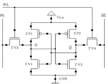
Figure 1. Conventional 6T SRAM cell.
The paper is organized as follows: Section 2 shows the design of the conventional 6T SRAM cell. Section 3 describes the circuit design and working principle of the proposed 8T SRAM cell for read operation. Section 4 elaborately discusses the simulation results of the pro-posed SRAM cell for Dynamic Noise Margin (DNM), Static Noise Margin (SNM), access time and power dissipation during the read operation, and, nally, Section 5 concludes the paper.
2. Conventional 6T SRAM cell
Figure 1 shows the circuit diagram of a conventional SRAM cell. Before the read operation begins, the bit line, BL, and the bitbar line, BL, are pre-charged to as high as Vdd. When the word line (WL) is selected,
the access transistors are turned on. This causes a current to ow from Vdd through the pull-up transistor
T P 1 of the node storing \1". On the other side, current will ow from the pre-charged BL to ground, thus, discharging the BL line. Thus, a dierential voltage develops between the BL and BL. This small potential dierence between the bit lines is sensed and amplied by the sense ampliers at the data output. A conventional 6T SRAM cell works on a full voltage swing. This means that if the operating frequency of the SRAM cell is increased, then, the dynamic power dissipation will also be increased. Hence, for high speed CMOS operation, the conventional SRAM cell is not a good choice. Also, a conventional 6T SRAM cell has been found to be unstable beyond below 130 nm technology, and results in a low read Static Noise Margin (SNM).
3. Proposed 8T SRAM cell
In order to overcome the problem associated with conventional 6T SRAM, this paper proposes a novel 8T SRAM architecture to achieve very low power
Figure 2. Proposed 8T SRAM cell.
dissipation and better stability. In the proposed design, two voltage sources, V 1 and V 2, are connected to the outputs of the bit line and the bitbar line, respectively. Two NMOS transistors, T N5 and T N6, are used. One is connected with the bit line and the other is connected with the bitbar line directly to switch ON and switch OFF the power source during write/read operations. The proposed design has been illustrated in Figure 2. These power sources reduce the voltage swing at the output node when the write/read operation is being performed.
The dynamic power may be expressed as: Pdynamic= CVddVSwingf; (1)
where:
C Load capacitance; Activity factor; f Clock frequency;
VSwing Voltage swing at the output node;
Vdd The power supply voltage.
So, in the conventional VLSI design, as the frequency increases, the dynamic power dissipation also increases, because the dynamic power depends on the operating frequency [40]. The two voltage sources, V 1 and V 2, reduce the swing voltage, which is used during the switching activity from \0" to \1" and vice-versa.
For performing the read operation in the proposed SRAM cell, a precharge circuit and sense amplier are used. Precharge circuits perform the precharge operation before the read operation starts. The sense amplier will produce the potential dierence between the bit line and the bitbar line and also amplify the signal during the read operation.
3.1. Precharge circuit
The circuit arrangement for the precharge circuit is shown in Figure 3. When an equalizing pulse is given
and T P 5 is used to equalize the voltage equally to the bit line and bitbar line. The purpose of the precharge circuit is to charge the bit line and bitbar line to supply voltage before the starting of the read operation. The precharging enables the bit-lines to be charged to Vdd
for the entire time period, except during the write operation.
3.2. Sense amplier
Sense ampliers are used to detect small currents that ow through the access transistors or the small voltage dierences that occur during charge sharing. For designing the sense ampliers, cross-coupled inverters are used to sense a small change of voltage on the bit line and the bitbar line. The arrangement for the sense amplier is shown in Figure 4.
Figure 3. Precharge circuit.
Figure 4. Sense amplier.
ampliers sense the dierence in voltage between the bit line and the bitbar line, and the output of the inverters is either `1' or `0', depending on the voltage levels sensed. The read circuit and the sense amplier are isolated from the remaining circuits by the two PMOS transistors, P 3 and P 4, connected between the bit line, the bitbar line and the sense amplier, respectively. The sizings of the transistors are done using the same ideology as that of the SRAM cell discussed earlier.
To perform the read operation in the proposed SRAM cell, rstly, the bit line and the bitbar line are charged to Vdd. The operation of precharging is
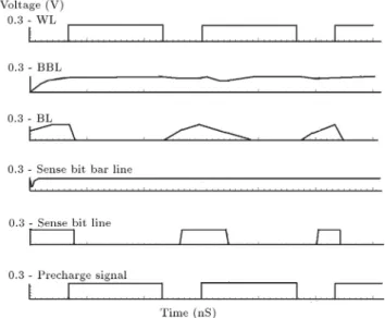
performed by the precharge circuit, shown in Figure 3. After that, the sense amplier is enabled to sense the voltage dierence between the bit line and the bitbar line. The sense amplier takes the dierence voltage or current of the bit line and the bitbar line and, nally, produces either `1' or `0' output, according to the voltage stored on the bit line and the bitbar line. Figure 5 shows the waveform during the read operation of the proposed 8T SRAM cell.
During switching activity from `0' to `1' or `1' to `0', the swing voltage is required at the bit line or the bitbar line. This extra voltage increases dynamic power dissipation. In the proposed 8T SRAM model, voltage sources, V 1 and V 2, reduce the voltage swing and improve the switching activity during write/read operation. As the frequency increases, the switching activity also increases, and this increases the dynamic power dissipation. But, the voltage source reduces its voltage swing simultaneously at the output. So, at higher frequency, the dynamic power dissipation
Figure 5. Read operation waveform of the proposed SRAM cell with sense amplier.
is found to be much less compared to other SRAM models reported in dierent literature. These two voltage sources also provide extra voltage during the write/read operation on the bit line, the bitbar line and the word line. The extra voltage will also provide a low voltage swing for the sense amplier during the read operation. Stability is also improved, due to the better switching capability of the proposed SRAM cell, as compared to other SRAM cells.
4. Simulation results and discussions
In this section, read static noise margin, read power dissipation, read access time and dynamic noise margin are calculated, and the simulated results are compared to those of other SRAM cells. Analog and schematic simulations have been done in a 45 nm environment, with the help of Microwind 3.1, by using the BSimM4 model.
4.1. Read Static Noise Margin (SNM) analysis
The stability of the SRAM cell is usually dened by the Static Noise Margin (SNM), which is the maximum value of DC noise voltage that can be tolerated by ip-ping the internal state. The read SNM of the proposed SRAM cell at 0.6 V is calculated and compared to that of dierent SRAM cells. For calculating the read static noise margin, the following equations are used [41]:
SNM =(NMH)2+ (NML)21=2; (2)
NMH= VOH VIH; (3)
NML= VIL VOL; (4)
where:
VIH Minimum high input voltage;
VIL Maximum low input voltage;
VOH Minimum high output voltage;
VOL Maximum low output voltage.
Table 1 shows the SNMs of dierent SRAM cells for the read operation. The read SNM for the proposed SRAM cell is 407 mV. From Figure 6, it is evident that the read SNM of the proposed SRAM cell has a higher value, as compared to the other SRAM cells. This justies the fact that the proposed SRAM cell is more stable for read operations than that of other cells. 4.2. Read power dissipation analysis
The proposed SRAM is simulated using 45 nm CMOS technology with a 0.3 V power supply, and the results for read power dissipation are compared to those of other existing SRAM cells. Comparison of the read powers of the proposed SRAM for read `0' and read `1'
Table 1. Read static noise margin for dierent SRAM cell.
Cell Read static noise margin (mV)
6T SRAM [5] 146
8T SRAM [7] 310
9T SRAM [8] 315
10T SRAM [1] 357
Proposed SRAM 407
Figure 6. Static noise margin comparison for read operation.
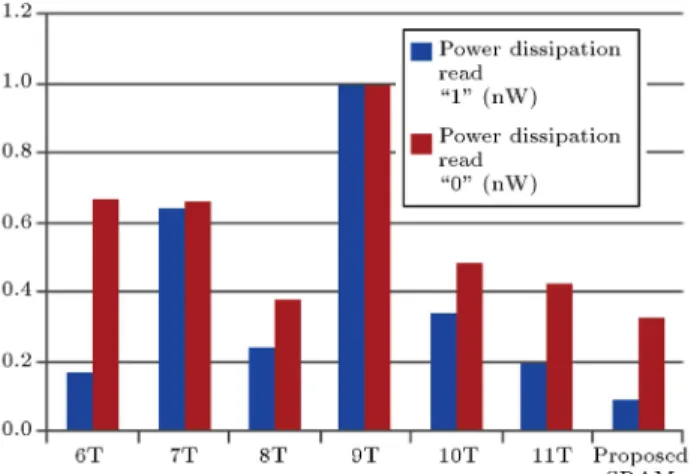
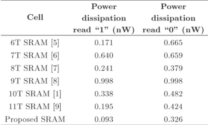
Figure 7. Read power dissipations in dierent SRAM cells.
is shown in Table 2. From Figure 7, it is evident that the proposed SRAM cell dissipates 0.093 nW, 0.326 nW of power for read \1" and read \0" operations, respec-tively. That means the proposed SRAM dissipates less power in comparison to all existing SRAM cells. 4.3. Read access time analysis
In this section, the read access time of the proposed SRAM cell is calculated and compared to that of existing SRAM cells. Access time has been calculated in a 45 nm technology environment with a 0.3 V power supply. Read access times for dierent SRAM cells are shown in Table 3. Table 3 shows that the read access time of the proposed SRAM cell is 359 pico seconds for the read operation.
read \1" (nW) read \0" (nW)
6T SRAM [5] 0.171 0.665
7T SRAM [6] 0.640 0.659
8T SRAM [7] 0.241 0.379
9T SRAM [8] 0.998 0.998
10T SRAM [1] 0.338 0.482
11T SRAM [9] 0.195 0.424
Proposed SRAM 0.093 0.326
Table 3. Read access times for dierent SRAM cells. Cell Read access time
(ps) 6T SRAM [5] 4.094
7T SRAM [6] 240
8T SRAM [7] 210
9T SRAM [8] 466
10T SRAM [1] 6.05
11T SRAM [9] 203
Proposed SRAM 359
Figure 8. Access time comparison for read operation.
Figure 8 shows that the read access time for the proposed SRAM cell is very much higher than that of the 6T and 10T SRAM cells. This is because the access time depends on the voltage swing, and, in the proposed SRAM cell, the voltage swing is reduced during the read operation. So, access time for the proposed SRAM cell is poorer than that of the other SRAM cells. But, the proposed 8T SRAM results in better access time than that of the 9T SRAM model proposed in [8].
proposed 8T SRAM cell. To dene the DNM, the rst concern is the criterion for a write failure. A write failure occurs when the write time is larger than the word line pulse width. The word line pulse width depends on a number of factors, such as the number of drivers of bit lines and the word line. Write time is dened as the time when the node storing `1' is pulled down from VDD to a critically low value. This write
failure denition is valid for most of the reasonable write cycles. Analysis of the DNMs for logic gates has shown that both noise amplitude and noise duration are critical for dynamic stability [42].
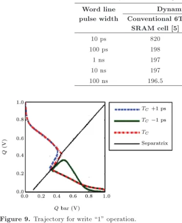
Static noise is pulsed noise with an innitely long pulse length. In general, it is found that the dynamic noise margins are larger than the static ones, because, during short pulses, higher noise amplitudes may be applied. Dynamic stability analysis was applied to the SRAM cell, which resulted in an analytical model for evaluating its dynamic noise margin while in the standby mode. This model assumes that the noise source is a current noise pulse injected into the node storing `0'. For a given noise amplitude, the model estimates the critical pulse width, i.e. the minimum pulse duration for the noise to ip the cell's state. Dynamic instability occurs when the injected noise causes the cell's state to follow a trajectory that crosses the boundary of attraction regions. In order to evaluate the write ability and read ability of a cell more precisely, a metric which takes the dynamic write/read behaviour into account must be used. On a successful write, Q and Q cross over and eventually settle at VDD
and 0V, respectively. The word line pulse width (Twl)
determines whether the two waveforms cross and the write is successful or not. This proposed 8T SRAM model uses the minimum world line pulse width (TC)
for the cell to ip ultimately to the correct new state as a metric for the dynamic write margin. Figure 9 shows the Trajectory for Write \1" Operation.
In order to understand TC as a useful metric,
let us relate it back to the dynamic stability analysis. Figure 10 shows the trajectories of Q and Q for writing `1', when Twlis equal to TC 1 ps, TC, and TC+ 1 ps.
The trajectories all overlap each other as they approach the separatrix, but they diverge at that point, because the word line pulses end at slightly dierent times. The two trajectories for Twl TC, then, overlap again,
as they converge to the newly written value, but, the trajectory for Twl< TC falls back to the starting state.
This simulation clearly shows that TC is the word line
pulse width that causes the state of the cell (Q; Q) to cross over the separatrix when the word line drops to 50% of Vdd. It may also be noted that variation has
Table 4. Dynamic noise margin variation with noise pulse width. Word line
pulse width
Dynamic noise margin (mV) Conventional 6T
SRAM cell [5]
10 SRAM cell [43]
Proposed 8T SRAM cell
10 ps 820 1460 1712
100 ps 198 390 540
1 ns 197 388 539.4
10 ns 197 388 539.1
100 ns 196.5 387.7 538.8
Figure 9. Trajectory for write \1" operation.
Figure 10. Monte-Carlo simulation curve for proposed SRAM cell.
variations will make TC dicult to predict, since both
the trajectories of the cell state during the word line pulse, and the separatrix of the cell, will vary with the device parameters.
The DNM of the proposed SRAM cell is 0.54 V at 100 ps wordline pulse width and its value at 100 ns is 0.538 V. So, the DNM value is almost constant as the wordline pulse increases. From Figure 10, it is evident that the density of the blue dots is higher in between 0.45 V and 0.6 V. This justies the fact that the stability of the proposed 8T SRAM cell is better between these voltage values. Reduction in
Figure 11. Dynamic noise margin comparison of SRAM cells.
swing voltage causes a reduction in dynamic power dissipation. Improvement in switching activity also improves the dynamic noise margin.
Table 4 shows the variation of DNM with respect to wordline pulse width time. Table 4 shows that when the pulse width time goes from 10 ps to 100 ps, the DNM goes down to 70% of its original value. After 100 ps of time, as the width time still increases, the DNM becomes almost constant. At this point, the DNM values get saturated and approach their SNM values. This arms that the proposed design is more stable compared to the conventional 6T and 10T SRAM cells. The comparison of DNMs among 6T, 10T cells and the proposed SRAM cell has been shown in Figure 11. Figure 11 shows that after 100 ps, all SRAM cells reach static conditions.
5. Conclusions
Power dissipation and stability will be major issues as the demand for high speed battery operated devices increases. In this paper, the dynamic noise margin, the read static noise margin, access time and power dissipation are analyzed during the read operation of the proposed 8T SRAM cell. These values are compared to those of dierent existing SRAM cells.
cells. Similarly, the proposed 8T SRAM cell dissipates 0.093 nW and 0.326 nW of power during read `1' and read `0' operations, respectively, which is much less than those of other existing SRAM cells. The dynamic noise margin for the proposed SRAM cell is 1712 mV at 10 ps, which shows that the proposed SRAM cell has better stability than the other compared SRAM cells. The read access time for the proposed SRAM is 359 ps, which is poorer than that of the other SRAM cells. This is because of the reduction in voltage swing. But, low power dissipation and higher stability can easily overcome this drawback. The proposed SRAM provides low power solution for high speed battery operated devices like laptops, biomedical equipment etc.
Acknowledgements
The authors sincerely thank NITTTR, Chandigarh, for providing Microwind 3.1 software to carry out this research.
References
1. Calhoun, B.H. and Chandrakasan, A. \A 256kb Sub-threshold SRAM in 65 nm CMOS", IEEE Inter-national Conference on Solid-State Circuits (ISSCC 2006), pp. 2592-2601 (2006).
2. Moradi, F., Wisland, D.T., Aunet, S., Mahmoodi, H. and Cao, T.V. \65 nm sub-threshold 11T-SRAM for ultra low voltage applications", IEEE International Conference on SOC, pp. 113-118 (2008).
3. Wang, A., Chandrakasan, A.P. and Kosonocky, S.V. \Optimal supply and threshold scaling for subthresh-old CMOS circuits", IEEE Computer Society Annual Symposium on VLSI, pp. 5-9 (2002).
4. Ramy, E. and Magdy, A.B. \Low-power cache design using 7T SRAM cell", IEEE Transactions on Circuits and Systems II, 54(4), pp. 318-322 (2007).
5. Singh, J., Pradhan, D.K., Hollis, S., Mohanty, S.P. and Mathew, J. \Single ended 6T SRAM with isolated read-port for low-power embedded systems", Confer-ence & Exhibition on Design Automation & Test, pp. 917-922 (2009).
6. Aly, R.E., Faisal, M.I. and Bayoumi, M.A. \Novel 7T SRAM cell for low power cache design", IEEE International Conference on SOC, pp. 171-174 (2005). 7. Chen, G., Sylvester, D., Blaauw, D. and Mudge, T. \Yield-driven near-threshold SRAM design", IEEE Transactions on Very Large Scale Integration (VLSI) Systems, 18(11), pp. 1590-1598 (2010).
8. Liu, Z. and Kursun, V. \Characterization of a novel nine-transistor SRAM cell", IEEE Transactions on
\A proposed symmetric and balanced 11-T SRAM cell for lower power consumption", IEEE Region 10 Conference on TENCON 2009, pp. 1-4 (2009). 10. Lin, S., Kim, Y.B. and Lombardi, F. \A low
leak-age 9T SRAM cell for ultra-low power operation", GLSVLSI'08, pp. 1-4 (2008).
11. Aly, R.E., Faisal, I. and Bayoumi, M.A. \ Novel 7T SRAM cell for low power cache design", In Proc. of SoCC., pp. 171-174 (2005).
12. Ming, G., Jun, Y. and Jun, X. \Low power SRAM de-sign using charge sharing technique", 6th International Conference on ASIC (ASICON), pp. 19-23 (2005). 13. Aly, R.E. and Bayoumi, M.A. \Low-power cache
design using 7T SRAM cell", IEEE Transactions on Circuits and Systems II, 54(4), pp. 318-322 (2007). 14. Wang, C., Lee, C. and Lin, W. \A 4-kb low-power
SRAM design with negative word-line scheme", IEEE Transactions on Circuits and Systems-I, 54(5), pp. 1069-1076 (2007).
15. Teman, A., Pergament, L., Cohen, O. and Fish, A. \A 250 mV 8 kb 40 nm ultra-low power 9T supply feedback SRAM (SF-SRAM)", IEEE Transactions on Circuits and Systems, 46(11), pp. 2713-2726 (2011). 16. Koc, F., Simsek, O.S. and Ergin, O. \Using
content-aware bitcells to reduce static energy dissipation", IEEE Intenational Conference on Computer Design, pp. 51-56 (2011).
17. Tawk, S.A. and Kursun, V. \Low power and robust 7T dual-Vt SRAM circuit", IEEE International Sym-posium on Circuits and Systems, pp. 1452-1455 (2008). 18. Kim, T.H., Liu, J., Keane, J. and Kim, C.H. \Circuit techniques for ultra-low power subthreshold SRAMs", IEEE International Symposium on Circuits and Sys-tems (ISCAS), pp. 2574-2577 (2008).
19. Gupta, V. and Anis, M. \Statistical design of the 6T SRAM bit cell", IEEE Transactions on Circuits and Systems-I, 57(1), pp. 93-104 (2010).
20. Do, A.T. Kong, Z.H., Yeo, K.S. and Shern, J.Y. \Design and sensitivity analysis of a new current-mode sense amplier for low-power SRAM", IEEE Transactions on Very Large Scale Integrations (VLSI) Systems, 19(2), pp. 196-204 (2011).
21. Singh, A.K., Prabhu, C.M.R., Pin, S.W. and Hou, T.C. \A proposed symmetric and balanced 11-T SRAM cell for lower power consumption", in Proc. IEEE TENCON, pp. 1-4 (2009).
22. Giraud, B., Amara, A. and Tkhomas, O. \An innova-tive 6T hybrid SRAM cell in sub-32 nm double-gate MOS technology", Fifth IEEE International Sympo-sium on Electronic Design, Test & Applications, pp. 241-244 (2010).
23. Azam, T., Cheng, B. and David R.S.C. \Variability resilient low-power 7T-SRAM design for nano-scaled technologies", 11th IEEE Internation Symposium on Quality Electronic Design, pp. 9-14 (2010).
24. Shukla, N., Mukherjee, D., Birla, S. and Singh, R.K. \Leakage current minimization in deep-submicron con-ventional single cell SRAM", IEEE International Con-ference on Recent Trends in Information, Telecommu-nication and Computing, pp. 381-383 (2010).
25. Cabe, A., Qi, Z. and Stan, M.R. \Stacking SRAM banks for ultra low power standby mode operation", 47th ACM/IEEE Design Automation Conference, pp. 699-705 (2010).
26. Kawasumi, A., Takeyama, Y., Hirabayashi, O., Kushida, K. Fujimura, Y. and Yabe, T. \A low-supply-voltage operation SRAM with HCI trimmed sense am-pliers", IEEE Journal of Solid-State Circuits, 45(11), pp. 2341-2347 (2010).
27. Teman, A. and Fish, A. \Sub-threshold and near-threshold SRAM design", IEEE 26th Convention of Electrical and Electronics Engineers in Israel, pp. 608-612 (2010).
28. Do, J., Shern, Y., Lih, J.Y., Kong, Z.H. Tan, X. and Yeo, K.S. \An 8T dierential SRAM with improved noise margin for bit-interleaving in 65 nm CMOS", IEEE Transactions on Circuits and Systems-I, 58(6), pp. 1252-1263 (2011).
29. Lo, C.H. and Huang, S.Y. \P-P-N based 10T SRAM cell for low-leakage and resilient subthreshold opera-tion", IEEE Journal of Solid-State Circuits, 46(3), pp. 695-704 (2011).
30. Calhoun, B.H. and Chandrakasan, A.P. \A 256-kb 65-nm subthreshold SRAM design for ultra-low-voltage operation", IEEE J. Solid-State Circuits, 42(3), pp. 680-688 (2007).
31. Lin, S., Kim, Y.B. and Lombardi, F. \A low leakage 9T SRAM cell for ultra-low power operation", Proc. GLSVLSI, pp. 123-126 (2008).
32. Kim, C.H., Kim, J.-J., Mukhopadhyay, S. and Roy, K. \A forward bodybiased low-leakage SRAM cache: Device, circuit and architecture considerations", IEEE Trans. VLSI Syst., 13(3), pp. 349-357 (2005). 33. Bogliolo, A., Benini, L., Lattanzi, E. and De Micheli,
G. \Specication and analysis of power-managed sys-tems", Proc. IEEE, 92(8), pp. 1308-1346 (2004). 34. Powell, M., Yang, S.H., Falsa, B., Roy, K. and
Vijaykumar, T.N. \Reducing leakage in a high-performance deep-submicron instruction cache", IEEE Trans. VLSI Syst., 9(1), pp. 77-89 (2001).
35. Agarwal, A., Li, H. and Roy, K. \DRG-cache: A data retention gatedground cache for low power", in Proc. ACM/IEEE DAC, pp. 473-478 (2002).
36. Makino, H., Shimizu, T. and Arakawa, T. \An auto-backgate-controlled MT-CMOS circuit", Proc. Sympo-sium VLSI Circuits, pp. 41-42 (1998).
37. Kim, C.H. and Roy, K. \Dynamic Vt SRAM: A leakage tolerant cache memory for low voltage microproces-sors", Proc. in ISLPED, pp. 251-254 (2002).
38. Shukla, N.K., Singh, R.K. and Pattanaik, M. \Design and analysis of a novel low-power SRAM bit-cell structure at deep-sub-micron CMOS technology for mobile multimedia applications", Int. J. Adv. Comp. Sci. Appl., 2(5), pp. 43-49 (2011).
39. Elakkumanan, P., Narasimhan, A. and Sridhar, R. \NC-SRAM-A low-leakage memory circuit for ultra deep submicron designs", in Proc. IEEE Int. SOC Conf., pp. 3-6 (2003).
40. Weste, H.E.N., Harris, D. and Banerjee, A. \CMOS VLSI Design", 3rd Edition, pp. 55-57, Pearson Educa-tion (2007).
41. Mishra, K. and Akashe, S. \Modeling and simula-tion of 7T SRAM cell at various process corners at 45 nm process technology", Second IEEE International Conference on Advanced Computing & Communication Technologies, pp. 361-363 (2012).
42. Lohstroh, J. \Static and dynamic noise margins of logic circuits", IEEE J. Solid-State Circuits, 14(3), pp. 591-598 (1979).
43. Singh, P., Sharma, S. and Sandhu, P.S. \A 16Kb 10T-SRAM with 4x read-power reduction", Journal of World Academy of Science, Engineering and Technol-ogy, 49(3), pp. 940-44 (2011).
Biographies
Prashant Upadhyay received a BE degree in Elec-tronics and Instrumentation Engineering from the Uni-versity Institute of Engineering and Technology, Dr. B. R. Ambedkar University, Agra, Uttar Pradesh, India in 2006, and a MTech degree in Electronics and Com-munication from the National Institute of Technical Teachers Training and Research, Chandigarh, India in 2010. Presently, he is attached with Maharishi Markandeshwar University, Solan, Himachal Pradesh, India, as Assistant Professor in the Department of Electronics and Communication Engineering, and is working towards a PhD degree in the Department of Electronics and Communication Engineering at NIT, Durgapur. His research interests include low power VLSI design. He has published more than 10 research papers in international journals and conferences. Rajib Kar received a BE degree in Electronics and Communication Engineering from the Regional En-gineering College, Durgapur, West Bengal, India, in 2001, and MTech and PhD degrees from the National Institute of Technology, Durgapur, West Bengal, In-dia, in 2008 and 2011, respectively. Presently, he is attached to the National Institute of Technology, Durgapur, West Bengal, India, as Assistant Professor in the Department of Electronics and Communication
210 research papers in international journals and con-ferences.
Durbadal Mandal received a BE degree in Electron-ics and Communication Engineering from the Regional Engineering College, Durgapur, West Bengal, India, in 1996. He obtained MTech and PhD degrees, in 2008 and 2011, respectively, from the National Institute of Technology, Durgapur, West Bengal, India, where he is currently Assistant Professor in the Department of Electronics and Communication Engineering. His re-search interests include array antenna design, and lter optimization via evolutionary computing techniques.
Sakti Prasad Ghoshal obtained BS and BTech degrees, in 1973 and 1977, respectively, from Calcutta University, West Bengal, India, an MTech degree from I.I.T (Kharagpur), in 1979, and a PhD degree from Jadavpur University, Kolkata, West Bengal, India, in 1992. Presently, he is Professor in the Electrical Engineering Department of N.I.T. Durgapur, West Bengal, India. His research interests include applica-tion of evoluapplica-tionary computing techniques to electrical power systems, digital signal processing, array antenna optimization and VLSI. He has published more than 200 research papers in international journals and con-ferences