Ultra-low-power Arm
®
Cortex
®
-M4 32-bit MCU+FPU, 100DMIPS,
up to 512KB Flash, 160KB SRAM, analog, audio, ext. SMPS
Datasheet-
production dataFeatures
• Ultra-low-power with FlexPowerControl – 1.71 V to 3.6 V power supply
– -40 °C to 85/125 °C temperature range – 145 nA in VBAT mode: supply for RTC and
32x32-bit backup registers
– 22 nA Shutdown mode (5 wakeup pins) – 106 nA Standby mode (5 wakeup pins) – 375 nA Standby mode with RTC
– 2.05 µA Stop 2 mode, 2.40 µA with RTC – 84 µA/MHz run mode (LDO Mode) – 36 μA/MHz run mode (@3.3 V SMPS
Mode)
– Batch acquisition mode (BAM) – 4 µs wakeup from Stop mode – Brown out reset (BOR) – Interconnect matrix
• Core: Arm® 32-bit Cortex®-M4 CPU with FPU, Adaptive real-time accelerator (ART
Accelerator™) allowing 0-wait-state execution from Flash memory, frequency up to 80 MHz, MPU, 100DMIPS and DSP instructions
• Performance benchmark
– 1.25 DMIPS/MHz (Drystone 2.1)
– 273.55 CoreMark® (3.42 CoreMark/MHz @ 80 MHz)
• Energy benchmark
– 335 ULPMark™ CP score – 104 ULPMark™ PP score
• Clock Sources
– 4 to 48 MHz crystal oscillator
– 32 kHz crystal oscillator for RTC (LSE) – Internal 16 MHz factory-trimmed RC (±1%) – Internal low-power 32 kHz RC (±5%) – Internal multispeed 100 kHz to 48 MHz
oscillator, auto-trimmed by LSE (better than ±0.25 % accuracy)
– Internal 48 MHz with clock recovery
– 2 PLLs for system clock, audio, ADC
• Up to 83 fast I/Os, most 5 V-tolerant
• RTC with HW calendar, alarms and calibration
• Up to 21 capacitive sensing channels: support touchkey, linear and rotary touch sensors
• 12x timers: 1x 16-bit advanced motor-control, 1x 32-bit and 3x bit general purpose, 2x 16-bit basic, 2x low-power 16-16-bit timers (available in Stop mode), 2x watchdogs, SysTick timer
• Memories
– Up to 512 KB single bank Flash, proprietary code readout protection – 160 KB of SRAM including 32 KB with
hardware parity check – Quad SPI memory interface
• Rich analog peripherals (independent supply) – 1x 12-bit ADC 5 Msps, up to 16-bit with
hardware oversampling, 200 µA/Msps – 1x 12-bit DAC output channels, low-power
sample and hold
– 1x operational amplifier with built-in PGA – 2x ultra-low-power comparators
– Accurate 2.5 V or 2.048 V reference voltage buffered output
• 17x communication interfaces
– USB 2.0 full-speed crystal less solution with LPM and BCD
– 1x SAI (serial audio interface)
– 4x I2C FM+(1 Mbit/s), SMBus/PMBus – 3x USARTs (ISO 7816, LIN, IrDA, modem) – 1x UART (LIN, IrDA, modem)
– 1x LPUART (Stop 2 wake-up) – 3x SPIs (and 1x Quad SPI)
– CAN (2.0B Active) and SDMMC interface
UFBGA100 (7×7) LQFP64 (10×10) UFBGA64 (5×5)
LQFP100 (14×14) WLCSP64 UFQFPN48 (7×7) (3.36×3.66)
– IRTIM (Infrared interface)
• 14-channel DMA controller
• True random number generator
• CRC calculation unit, 96-bit unique ID
• Development support: serial wire debug (SWD), JTAG, Embedded Trace Macrocell™
• All packages are ECOPACK2® compliant
Table 1. Device summary
Reference Part numbers
Contents
1
Introduction . . . 12
2
Description . . . 13
3
Functional overview . . . 17
3.1
Arm
®Cortex
®-M4 core with FPU . . . 17
3.2
Adaptive real-time memory accelerator (ART Accelerator™) . . . 17
3.3
Memory protection unit . . . 17
3.4
Embedded Flash memory . . . 18
3.5
Embedded SRAM . . . 19
3.6
Firewall . . . 19
3.7
Boot modes . . . 20
3.8
Cyclic redundancy check calculation unit (CRC) . . . 20
3.9
Power supply management . . . 20
3.9.1 Power supply schemes . . . 20
3.9.2 Power supply supervisor . . . 22
3.9.3 Voltage regulator . . . 23
3.9.4 Low-power modes . . . 23
3.9.5 Reset mode . . . 31
3.9.6 VBAT operation . . . 31
3.10
Interconnect matrix . . . 32
3.11
Clocks and startup . . . 34
3.12
General-purpose inputs/outputs (GPIOs) . . . 37
3.13
Direct memory access controller (DMA) . . . 37
3.14
Interrupts and events . . . 38
3.14.1 Nested vectored interrupt controller (NVIC) . . . 38
3.14.2 Extended interrupt/event controller (EXTI) . . . 38
3.15
Analog to digital converter (ADC) . . . 39
3.15.1 Temperature sensor . . . 39
3.15.2 Internal voltage reference (VREFINT) . . . 40
3.15.3 VBAT battery voltage monitoring . . . 40
3.17
Voltage reference buffer (VREFBUF) . . . 41
3.18
Comparators (COMP) . . . 42
3.19
Operational amplifier (OPAMP) . . . 42
3.20
Touch sensing controller (TSC) . . . 42
3.21
Digital filter for Sigma-Delta Modulators (DFSDM) . . . 43
3.22
Random number generator (RNG) . . . 45
3.23
Timers and watchdogs . . . 45
3.23.1 Advanced-control timer (TIM1) . . . 46
3.23.2 General-purpose timers (TIM2, TIM3, TIM15, TIM16) . . . 46
3.23.3 Basic timer (TIM6) . . . 46
3.23.4 Low-power timer (LPTIM1 and LPTIM2) . . . 47
3.23.5 Infrared interface (IRTIM) . . . 47
3.23.6 Independent watchdog (IWDG) . . . 47
3.23.7 System window watchdog (WWDG) . . . 47
3.23.8 SysTick timer . . . 48
3.24
Real-time clock (RTC) and backup registers . . . 48
3.25
Inter-integrated circuit interface (I
2C) . . . 49
3.26
Universal synchronous/asynchronous receiver transmitter (USART) . . . 50
3.27
Low-power universal asynchronous receiver transmitter (LPUART) . . . . 51
3.28
Serial peripheral interface (SPI) . . . 52
3.29
Serial audio interfaces (SAI) . . . 52
3.30
Controller area network (CAN) . . . 53
3.31
Secure digital input/output and MultiMediaCards Interface (SDMMC) . . . 53
3.32
Universal serial bus (USB) . . . 54
3.33
Clock recovery system (CRS) . . . 54
3.34
Quad SPI memory interface (QUADSPI) . . . 54
3.35
Development support . . . 56
3.35.1 Serial wire JTAG debug port (SWJ-DP) . . . 56
3.35.2 Embedded Trace Macrocell™ . . . 56
4
Pinouts and pin description . . . 57
5
Memory mapping . . . 86
6.1
Parameter conditions . . . 90
6.1.1 Minimum and maximum values . . . 90
6.1.2 Typical values . . . 90
6.1.3 Typical curves . . . 90
6.1.4 Loading capacitor . . . 90
6.1.5 Pin input voltage . . . 90
6.1.6 Power supply scheme . . . 91
6.1.7 Current consumption measurement . . . 92
6.2
Absolute maximum ratings . . . 92
6.3
Operating conditions . . . 95
6.3.1 General operating conditions . . . 95
6.3.2 Operating conditions at power-up / power-down . . . 96
6.3.3 Embedded reset and power control block characteristics . . . 96
6.3.4 Embedded voltage reference . . . 99
6.3.5 Supply current characteristics . . . 101
6.3.6 Wakeup time from low-power modes and voltage scaling transition times . . . 125
6.3.7 External clock source characteristics . . . 128
6.3.8 Internal clock source characteristics . . . 133
6.3.9 PLL characteristics . . . 140
6.3.10 Flash memory characteristics . . . 141
6.3.11 EMC characteristics . . . 142
6.3.12 Electrical sensitivity characteristics . . . 143
6.3.13 I/O current injection characteristics . . . 144
6.3.14 I/O port characteristics . . . 145
6.3.15 NRST pin characteristics . . . 150
6.3.16 Extended interrupt and event controller input (EXTI) characteristics . . 151
6.3.17 Analog switches booster . . . 151
6.3.18 Analog-to-Digital converter characteristics . . . 152
6.3.19 Digital-to-Analog converter characteristics . . . 165
6.3.20 Voltage reference buffer characteristics . . . 170
6.3.21 Comparator characteristics . . . 172
6.3.22 Operational amplifiers characteristics . . . 173
6.3.23 Temperature sensor characteristics . . . 176
6.3.24 VBAT monitoring characteristics . . . 177
6.3.25 Timer characteristics . . . 177
7
Package information . . . 191
7.1
LQFP100 package information . . . 191
7.2
UFBGA100 package information . . . 194
7.3
LQFP64 package information . . . 197
7.4
UFBGA64 package information . . . 199
7.5
WLCSP64 package information . . . 202
7.6
UFQFPN48 package information . . . 206
7.7
Thermal characteristics . . . 209
7.7.1 Reference document . . . 209
7.7.2 Selecting the product temperature range . . . 209
8
Ordering information . . . 212
List of tables
Table 1. Device summary . . . 2
Table 2. STM32L452xx family device features and peripheral counts . . . 14
Table 3. Access status versus readout protection level and execution modes. . . 18
Table 4. STM32L452xx modes overview . . . 24
Table 5. Functionalities depending on the working mode. . . 29
Table 6. STM32L452xx peripherals interconnect matrix . . . 32
Table 7. DMA implementation . . . 37
Table 8. Temperature sensor calibration values. . . 40
Table 9. Internal voltage reference calibration values . . . 40
Table 10. DFSDM1 implementation . . . 45
Table 11. Timer feature comparison . . . 45
Table 12. I2C implementation . . . 49
Table 13. STM32L452xx USART/UART/LPUART features . . . 50
Table 14. SAI implementation. . . 53
Table 15. Legend/abbreviations used in the pinout table . . . 61
Table 16. STM32L452xx pin definitions . . . 62
Table 17. Alternate function AF0 to AF7. . . 74
Table 18. Alternate function AF8 to AF15. . . 80
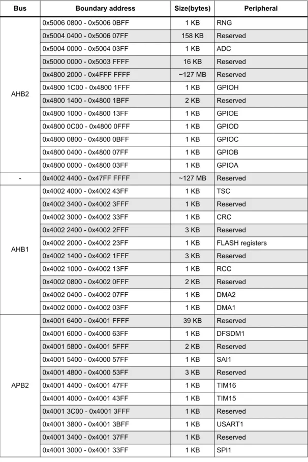
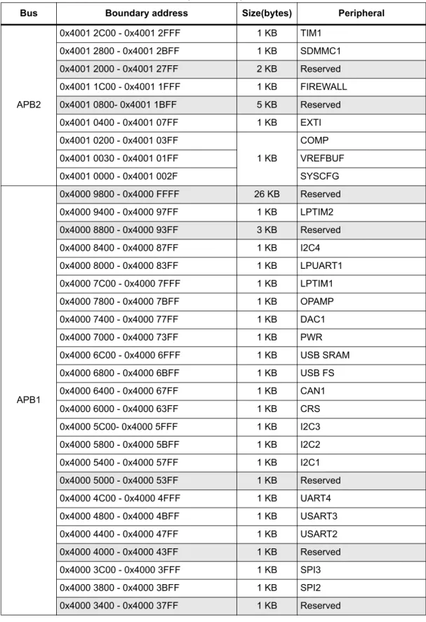
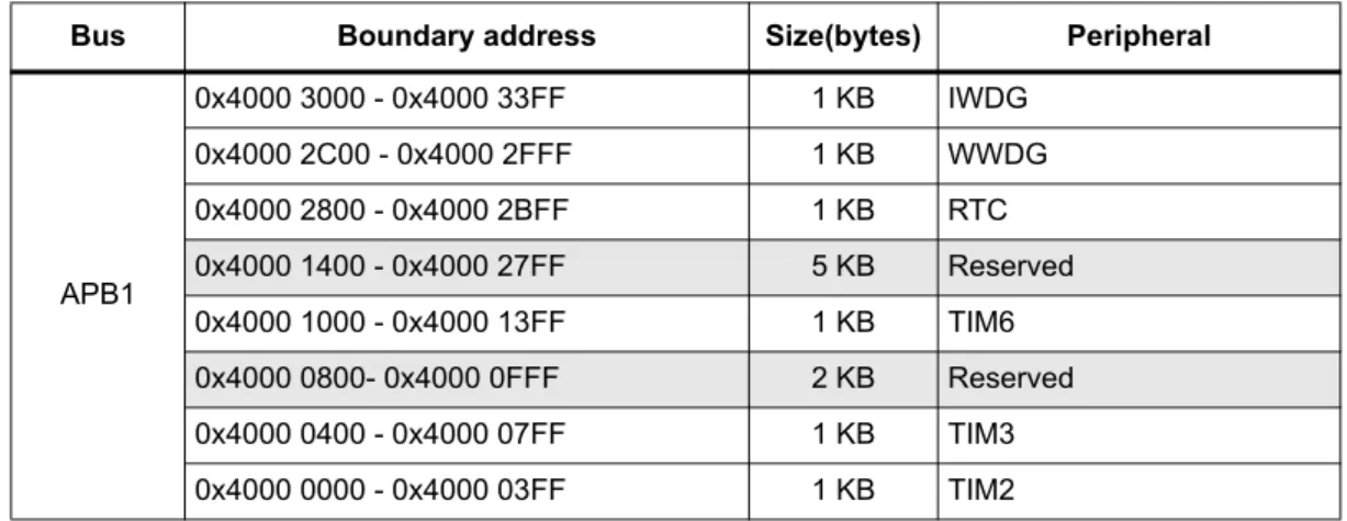
Table 19. STM32L452xx memory map and peripheral register boundary addresses . . . 87
Table 20. Voltage characteristics . . . 92
Table 21. Current characteristics . . . 93
Table 22. Thermal characteristics. . . 94
Table 23. General operating conditions . . . 95
Table 24. Operating conditions at power-up / power-down . . . 96
Table 25. Embedded reset and power control block characteristics. . . 96
Table 26. Embedded internal voltage reference. . . 99
Table 27. Current consumption in Run and Low-power run modes, code with data processing running from Flash, ART enable (Cache ON Prefetch OFF) . . . 102
Table 28. Current consumption in Run modes, code with data processing running from Flash, ART enable (Cache ON Prefetch OFF) and power supplied by external SMPS (VDD12 = 1.10 V) . . . 103
Table 29. Current consumption in Run and Low-power run modes, code with data processing running from Flash, ART disable . . . 104
Table 30. Current consumption in Run modes, code with data processing running from Flash, ART disable and power supplied by external SMPS (VDD12 = 1.10 V). . . 105
Table 31. Current consumption in Run and Low-power run modes, code with data processing running from SRAM1 . . . 106
Table 32. Current consumption in Run, code with data processing running from SRAM1 and power supplied by external SMPS (VDD12 = 1.10 V) . . . 107
Table 33. Typical current consumption in Run and Low-power run modes, with different codes running from Flash, ART enable (Cache ON Prefetch OFF) . . . 108
Table 34. Typical current consumption in Run, with different codes running from Flash, ART enable (Cache ON Prefetch OFF) and power supplied by external SMPS (VDD12 = 1.10 V) . . . 108
Table 35. Typical current consumption in Run, with different codes running from Flash, ART enable (Cache ON Prefetch OFF) and power supplied by external SMPS (VDD12 = 1.05 V) . . . 109 Table 36. Typical current consumption in Run and Low-power run modes, with different codes
running from Flash, ART disable . . . 110
Table 37. Typical current consumption in Run modes, with different codes running from Flash, ART disable and power supplied by external SMPS (VDD12 = 1.10 V) . . . 110
Table 38. Typical current consumption in Run modes, with different codesrunning from Flash, ART disable and power supplied by external SMPS (VDD12 = 1.05 V) . . . 111
Table 39. Typical current consumption in Run and Low-power run modes, with different codes running from SRAM1 . . . 111
Table 40. Typical current consumption in Run, with different codesrunning from SRAM1 and power supplied by external SMPS (VDD12 = 1.10 V) . . . 112
Table 41. Typical current consumption in Run, with different codesrunning from SRAM1 and power supplied by external SMPS (VDD12 = 1.05 V) . . . 112
Table 42. Current consumption in Sleep and Low-power sleep modes, Flash ON . . . 113
Table 43. Current consumption in Sleep, Flash ON and power supplied by external SMPS (VDD12 = 1.10 V) . . . 114
Table 44. Current consumption in Low-power sleep modes, Flash in power-down . . . 114
Table 45. Current consumption in Stop 2 mode . . . 115
Table 46. Current consumption in Stop 1 mode . . . 117
Table 47. Current consumption in Stop 0 . . . 118
Table 48. Current consumption in Standby mode . . . 119
Table 49. Current consumption in Shutdown mode . . . 120
Table 50. Current consumption in VBAT mode . . . 121
Table 51. Peripheral current consumption . . . 123
Table 52. Low-power mode wakeup timings . . . 125
Table 53. Regulator modes transition times . . . 127
Table 54. Wakeup time using USART/LPUART . . . 127
Table 55. High-speed external user clock characteristics. . . 128
Table 56. Low-speed external user clock characteristics . . . 129
Table 57. HSE oscillator characteristics . . . 130
Table 58. LSE oscillator characteristics (fLSE = 32.768 kHz) . . . 131
Table 59. HSI16 oscillator characteristics. . . 133
Table 60. MSI oscillator characteristics . . . .135
Table 61. HSI48 oscillator characteristics. . . 138
Table 62. LSI oscillator characteristics . . . 139
Table 63. PLL, PLLSAI1 characteristics . . . 140
Table 64. Flash memory characteristics . . . 141
Table 65. Flash memory endurance and data retention . . . 141
Table 66. EMS characteristics . . . 142
Table 67. EMI characteristics . . . 143
Table 68. ESD absolute maximum ratings . . . 143
Table 69. Electrical sensitivities . . . 144
Table 70. I/O current injection susceptibility . . . 144
Table 71. I/O static characteristics . . . 145
Table 72. Output voltage characteristics . . . 147
Table 73. I/O AC characteristics . . . 148
Table 74. NRST pin characteristics . . . 150
Table 75. EXTI Input Characteristics . . . 151
Table 76. Analog switches booster characteristics . . . 151
Table 77. ADC characteristics . . . 152
Table 78. Maximum ADC RAIN . . . 154
Table 79. ADC accuracy - limited test conditions 1 . . . 156
Table 80. ADC accuracy - limited test conditions 2 . . . 158
Table 82. ADC accuracy - limited test conditions 4 . . . 162
Table 83. DAC characteristics . . . 165
Table 84. DAC accuracy. . . 168
Table 85. VREFBUF characteristics . . . 170
Table 86. COMP characteristics . . . 172
Table 87. OPAMP characteristics . . . 173
Table 88. TS characteristics . . . 176
Table 89. VBAT monitoring characteristics . . . 177
Table 90. VBAT charging characteristics . . . 177
Table 91. TIMx characteristics . . . 177
Table 92. IWDG min/max timeout period at 32 kHz (LSI). . . 178
Table 93. WWDG min/max timeout value at 80 MHz (PCLK). . . 178
Table 94. I2C analog filter characteristics. . . 179
Table 95. SPI characteristics . . . 180
Table 96. Quad SPI characteristics in SDR mode . . . 183
Table 97. QUADSPI characteristics in DDR mode . . . 184
Table 98. SAI characteristics . . . 186
Table 99. SD / MMC dynamic characteristics, VDD=2.7 V to 3.6 V . . . 188
Table 100. eMMC dynamic characteristics, VDD = 1.71 V to 1.9 V . . . 189
Table 101. USB electrical characteristics . . . 190
Table 102. LQPF - 100-pin, 14 x 14 mm low-profile quad flat package mechanical data . . . 191
Table 103. UFBGA - 100-ball, 7 x 7 mm, 0.50 mm pitch, ultra fine pitch ball grid array package mechanical data . . . 194
Table 104. UFBGA100 recommended PCB design rules (0.5 mm pitch BGA) . . . 195
Table 105. LQFP - 64 pins, 10 x 10 mm low-profile quad flat package mechanical data . . . 197
Table 106. UFBGA – 64 balls, 5 x 5 mm, 0.5 mm pitch ultra profile fine pitch ball grid array package mechanical data . . . 200
Table 107. UFBGA64 recommended PCB design rules (0.5 mm pitch BGA) . . . 201
Table 108. WLCSP - 64 balls, 3.357x3.657 mm 0.4 mm pitch wafer level chip scale mechanical data . . . 203
Table 109. WLCSP64 recommended PCB design rules (0.4 mm pitch) . . . 204
Table 110. UFQFPN - 48 leads, 7x7 mm, 0.5 mm pitch, ultra thin fine pitch quad flat package mechanical data . . . 207
Table 111. Package thermal characteristics . . . 209
Table 112. STM32L452xx ordering information scheme . . . 212
List of figures
Figure 1. STM32L452xx block diagram . . . 16
Figure 2. Power supply overview . . . 21
Figure 3. Power-up/down sequence . . . 22
Figure 4. Clock tree . . . 36
Figure 5. Voltage reference buffer . . . 41
Figure 6. STM32L452Vx LQFP100 pinout(1). . . 57
Figure 7. STM32L452Vx UFBGA100 ballout(1) . . . 58
Figure 8. STM32L452Rx LQFP64 pinout(1). . . 58
Figure 9. STM32L452Rx, external SMPS device, LQFP64 pinout(1). . . 59
Figure 10. STM32L452Rx UFBGA64 ballout(1). . . 59
Figure 11. STM32L452Rx WLCSP64 pinout(1) . . . 60
Figure 12. STM32L452Rx, external SMPS device, WLCSP64 pinout(1). . . 60
Figure 13. STM32L452Cx UFQFPN48 pinout(1) . . . 61
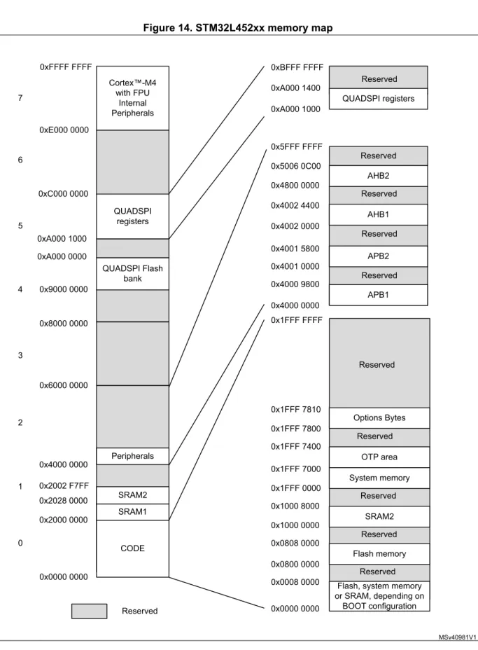
Figure 14. STM32L452xx memory map. . . 86
Figure 15. Pin loading conditions. . . 90
Figure 16. Pin input voltage . . . 90
Figure 17. Power supply scheme. . . 91
Figure 18. Current consumption measurement scheme with and without external SMPS power supply . . . 92
Figure 19. VREFINT versus temperature . . . 100
Figure 20. High-speed external clock source AC timing diagram . . . 128
Figure 21. Low-speed external clock source AC timing diagram . . . 129
Figure 22. Typical application with an 8 MHz crystal . . . 131
Figure 23. Typical application with a 32.768 kHz crystal . . . 132
Figure 24. HSI16 frequency versus temperature . . . 134
Figure 25. Typical current consumption versus MSI frequency . . . 138
Figure 26. HSI48 frequency versus temperature . . . 139
Figure 27. I/O input characteristics . . . 146
Figure 28. I/O AC characteristics definition(1) . . . 150
Figure 29. Recommended NRST pin protection . . . 151
Figure 30. ADC accuracy characteristics . . . 163
Figure 31. Typical connection diagram using the ADC . . . 164
Figure 32. 12-bit buffered / non-buffered DAC. . . 167
Figure 33. SPI timing diagram - slave mode and CPHA = 0 . . . 181
Figure 34. SPI timing diagram - slave mode and CPHA = 1 . . . 182
Figure 35. SPI timing diagram - master mode . . . 182
Figure 36. Quad SPI timing diagram - SDR mode . . . 185
Figure 37. Quad SPI timing diagram - DDR mode. . . 185
Figure 38. SAI master timing waveforms . . . 187
Figure 39. SAI slave timing waveforms . . . 188
Figure 40. SDIO high-speed mode . . . 189
Figure 41. SD default mode . . . 190
Figure 42. LQFP - 100-pin, 14 x 14 mm low-profile quad flat package outline . . . 191
Figure 43. LQFP - 100-pin, 14 x 14 mm low-profile quad flat recommended footprint . . . 192
Figure 44. LQFP100 marking (package top view) . . . 193
Figure 45. UFBGA - 100-ball, 7 x 7 mm, 0.50 mm pitch, ultra fine pitch ball grid array package outline . . . 194
Figure 46. UFBGA100 - 100-ball, 7 x 7 mm, 0.50 mm pitch, ultra fine pitch ball grid
array package recommended footprint . . . 195 Figure 47. UFBGA100 marking (package top view) . . . 196 Figure 48. LQFP - 64 pins, 10 x 10 mm low-profile quad flat package outline. . . 197 Figure 49. LQFP - 64 pins, 10 x 10 mm low-profile quad flat package
recommended footprint . . . 198 Figure 50. LQFP64 marking (package top view) . . . 199 Figure 51. UFBGA – 64 balls, 5 x 5 mm, 0.5 mm pitch ultra profile fine pitch ball grid
array package outline . . . 199 Figure 52. UFBGA64 – 64 balls, 5 x 5 mm, 0.5 mm pitch ultra profile fine pitch ball grid
array package recommended footprint . . . 200 Figure 53. UFBGA64 marking (package top view) . . . 201 Figure 54. WLCSP - 64 balls, 3.357x3.657 mm 0.4 mm pitch wafer level chip scale
package outline. . . 202 Figure 55. WLCSP - 64 balls, 3.357x3.657 mm 0.4 mm pitch wafer level chip scale
recommended footprint . . . 203 Figure 56. WLCSP64 marking (package top view) . . . 204 Figure 57. WLCSP64, external SMPS device, marking (package top view) . . . 205 Figure 58. UFQFPN - 48 leads, 7x7 mm, 0.5 mm pitch, ultra thin fine pitch quad flat
package outline. . . 206 Figure 59. UFQFPN - 48 leads, 7x7 mm, 0.5 mm pitch, ultra thin fine pitch quad flat
package recommended footprint . . . 207 Figure 60. UFQFPN48 marking (package top view) . . . 208 Figure 61. LQFP64 PD max vs. TA . . . 211
1 Introduction
This datasheet provides the ordering information and mechanical device characteristics of the STM32L452xx microcontrollers.
This document should be read in conjunction with the STM32L43xxx/44xxx/45xxx/46xxx reference manual (RM0394). The reference manual is available from the
STMicroelectronics website www.st.com.
For information on the Arm®(a) Cortex®-M4 core, please refer to the Cortex®-M4 Technical Reference Manual, available from the www.arm.com website.
2 Description
The STM32L452xx devices are the ultra-low-power microcontrollers based on the high-performance Arm® Cortex®-M4 32-bit RISC core operating at a frequency of up to 80 MHz. The Cortex-M4 core features a Floating point unit (FPU) single precision which supports all Arm® single-precision data-processing instructions and data types. It also implements a full set of DSP instructions and a memory protection unit (MPU) which enhances application security.
The STM32L452xx devices embed high-speed memories (Flash memory up to 512 Kbyte, 160 Kbyte of SRAM), a Quad SPI flash memories interface (available on all packages) and an extensive range of enhanced I/Os and peripherals connected to two APB buses, two AHB buses and a 32-bit multi-AHB bus matrix.
The STM32L452xx devices embed several protection mechanisms for embedded Flash memory and SRAM: readout protection, write protection, proprietary code readout protection and Firewall.
The devices offer a fast 12-bit ADC (5 Msps), two comparators, one operational amplifier, one DAC channel, an internal voltage reference buffer, a low-power RTC, one general-purpose 32-bit timer, one 16-bit PWM timer dedicated to motor control, four general-general-purpose 16-bit timers, and two 16-bit low-power timers.
In addition, up to 21 capacitive sensing channels are available. They also feature standard and advanced communication interfaces.
• Four I2Cs
• Three SPIs
• Three USARTs, one UART and one Low-Power UART.
• One SAI (Serial Audio Interfaces)
• One SDMMC
• One CAN
• One USB full-speed device crystal less
The STM32L452xx operates in the -40 to +85 °C (+105 °C junction) and -40 to +125 °C (+130 °C junction) temperature ranges from a 1.71 to 3.6 V VDD power supply when using internal LDO regulator and a 1.05 to 1.32V VDD12 power supply when using external SMPS supply. A comprehensive set of power-saving modes allows the design of low-power applications.
Some independent power supplies are supported: analog independent supply input for ADC, DAC, OPAMP and comparators. A VBAT input allows to backup the RTC and backup registers. Dedicated VDD12 power supplies can be used to bypass the internal LDO
regulator when connected to an external SMPS.
Table 2. STM32L452xx family device features and peripheral counts
Peripheral STM32L452Vx STM32L452Rx STM32L452Cx
Flash memory 256KB 512KB 256KB 512KB 256KB 512KB
SRAM 160KB
Quad SPI Yes
Timers
Advanced
control 1 (16-bit)
General purpose
2 (16-bit) 1 (32-bit)
Basic 2 (16-bit)
Low -power 2 (16-bit)
SysTick timer 1
Watchdog timers (independent, window)
2
Comm. interfaces
SPI 3
I2C 4
USART UART LPUART
3 1 1
SAI 1
CAN 1
USB FS Yes
SDMMC Yes(1) No
RTC Yes
Tamper pins 3 2 2
Random generator Yes
GPIOs(2) Wakeup pins
83 5
52 4(1)
38 3 Capacitive sensing
Number of channels 21 12 6
12-bit ADC
Number of channels
1 16
1 16(1)
1 10
12-bit DAC channels 1
Internal voltage reference
buffer Yes No
Analog comparator 2
Operational amplifiers 1
Operating voltage 1.71 to 3.6 V
Operating temperature
Ambient operating temperature: -40 to 85 °C / -40 to 125 °C
Junction temperature: -40 to 105 °C / -40 to 130 °C
Packages LQFP100
UFBGA100
WLCSP64 LQFP64 UFBGA64
UFQFPN48
1. WKUP5, ADC1_IN14 and SDMMC interface are not supported by 64-pin packages with SMPS option. 2. In case external SMPS package type is used, 2 GPIO's are replaced by VDD12 pins to connect the SMPS
power supplies hence reducing the number of available GPIO's by 2.
Table 2. STM32L452xx family device features and peripheral counts (continued)
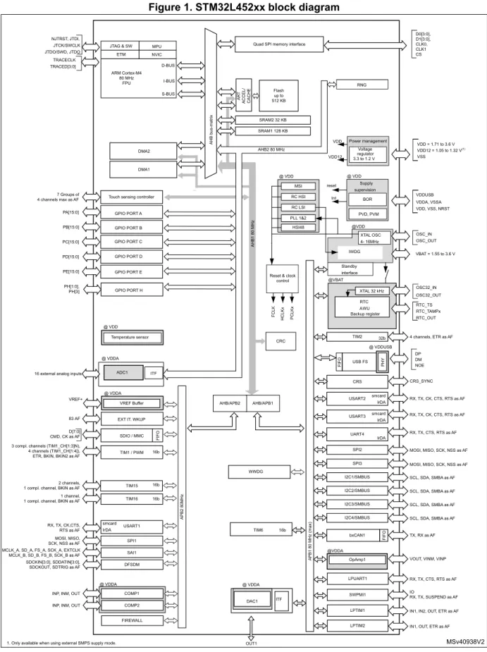
Figure 1. STM32L452xx block diagram
Note: AF: alternate function on I/O pins.
MSv40938V2 Flash
up to 512 KB
DAC1 GPIO PORT A
EXT IT. WKUP 83 AF
PA[15:0]
TIM1 / PWM 3 compl. channels (TIM1_CH[1:3]N),
4 channels (TIM1_CH[1:4]), ETR, BKIN, BKIN2 as AF
USART1 RX, TX, CK,CTS,
RTS as AF
SPI1 MOSI, MISO,
SCK, NSS as AF
AP B2 60 M H z AP B1 3 0 M H z ITF WWDG RTC_TS OSC32_IN OSC32_OUT smcard IrDA 16b SDIO / MMC D[7:0]
CMD, CK as AF
VBAT = 1.55 to 3.6 V JTAG & SW
ARM Cortex-M4 80 MHz FPU NVIC ETM MPU DMA2 AR T ACCEL/ CACHE RNG FIFO @ VDDA BOR Supply supervision PVD, PVM Int reset
XTAL 32 kHz M AN A G T
RTC FCLK Standby interface IWDG @VBAT @ VDD @VDD AWU Reset & clock
control PCLKx @ VDD RTC_TAMPx Backup register AHB bus-matrix TIM15 2 channels,
1 compl. channel, BKIN as AF
TIM6
TIM2 D-BUS
SRAM2 32 KB
APB1 80 MHz (max)
SRAM1 128 KB I-BUS S-BUS DMA1 PB[15:0] PC[15:0] PD[15:0] PE[15:0] PH[1:0], PH[3]
GPIO PORT B GPIO PORT C
GPIO PORT D
GPIO PORT E
GPIO PORT H
16b
TIM16 16b
1 channel, 1 compl. channel, BKIN as AF
16b
32b 4 channels, ETR as AF
OSC_IN OSC_OUT
HCLKx
XTAL OSC 4- 16MHz
16 external analog inputs
VREF+
U S AR T 2 M B p sTemperature sensor
@ VDDA
SAI1 MCLK_A, SD_A, FS_A, SCK_A, EXTCLK
MCLK_B, SD_B, FS_B, SCK_B as AF
Touch sensing controller 7 Groups of
4 channels max as AF RC HSI
RC LSI PLL 1&2 MSI Quad SPI memory interface
D0[3:0], D1[3:0], CLK0, CLK1 CS COMP1 INP, INM, OUT
COMP2 INP, INM, OUT
@ VDDA
RTC_OUT
AHB1 80 MHz
CRC
APB2 80MHz
AHB2 80 MHz
FIREWALL VREF Buffer @ VDDA @ VDD
VDDA, VSSA VDD, VSS, NRST VDDUSB TRACECLK TRACED[3:0] NJTRST, JTDI, JTCK/SWCLK JTDO/SWD, JTDO ITF ADC1 HSI48 AHB/APB1 AHB/APB2
VOUT, VINM, VINP OpAmp1
@VDDA
FIFO TX, RX as AF
bxCAN1
SCL, SDA, SMBA as AF I2C3/SMBUS
SCL, SDA, SMBA as AF I2C2/SMBUS
I2C1/SMBUS SCL, SDA, SMBA as AF
MOSI, MISO, SCK, NSS as AF SPI3
MOSI, MISO, SCK, NSS as AF SPI2
USART3 smcard RX, TX, CK, CTS, RTS as AF
IrDA
USART2 smcard RX, TX, CK, CTS, RTS as AF
IrDA CRS CRS_SYNC USB FS @ VDDUSB FIFO PHY DP DM NOE
LPUART1 RX, TX, CTS, RTS as AF
SWPMI1 IO
RX, TX, SUSPEND as AF
LPTIM1 IN1, IN2, OUT, ETR as AF
LPTIM2 IN1, OUT, ETR as AF
SCL, SDA, SMBA as AF I2C4/SMBUS
DFSDM SDCKIN[3:0], SDDATIN[3:0],
SDCKOUT, SDTRIG as AF
UART4 RX, TX, CTS, RTS as AF
IrDA
OUT1
Voltage regulator 3.3 to 1.2 V
VDD Power management
VDD = 1.71 to 3.6 V VSS
VDD12 = 1.05 to 1.32 V(1)
VDD12
3 Functional
overview
3.1 Arm
®
Cortex
®
-M4 core with FPU
The Arm® Cortex®-M4 with FPU processor is the latest generation of Arm® processors for embedded systems. It was developed to provide a low-cost platform that meets the needs of MCU implementation, with a reduced pin count and low-power consumption, while
delivering outstanding computational performance and an advanced response to interrupts. The Arm® Cortex®-M4 with FPU 32-bit RISC processor features exceptional
code-efficiency, delivering the high-performance expected from an Arm® core in the memory size usually associated with 8- and 16-bit devices.
The processor supports a set of DSP instructions which allow efficient signal processing and complex algorithm execution.
Its single precision FPU speeds up software development by using metalanguage development tools, while avoiding saturation.
With its embedded Arm® core, the STM32L452xx family is compatible with all Arm® tools and software.
Figure 1 shows the general block diagram of the STM32L452xx family devices.
3.2
Adaptive real-time memory accelerator (ART Accelerator™)
The ART Accelerator™ is a memory accelerator which is optimized for STM32 industry-standard Arm® Cortex®-M4 processors. It balances the inherent performance advantage of the Arm® Cortex®-M4 over Flash memory technologies, which normally requires the processor to wait for the Flash memory at higher frequencies.
To release the processor near 100 DMIPS performance at 80MHz, the accelerator implements an instruction prefetch queue and branch cache, which increases program execution speed from the 64-bit Flash memory. Based on CoreMark benchmark, the performance achieved thanks to the ART accelerator is equivalent to 0 wait state program execution from Flash memory at a CPU frequency up to 80 MHz.
3.3
Memory protection unit
The memory protection unit (MPU) is used to manage the CPU accesses to memory to prevent one task to accidentally corrupt the memory or resources used by any other active task. This memory area is organized into up to 8 protected areas that can in turn be divided up into 8 subareas. The protection area sizes are between 32 bytes and the whole 4 gigabytes of addressable memory.
The MPU is especially helpful for applications where some critical or certified code has to be protected against the misbehavior of other tasks. It is usually managed by an RTOS (real-time operating system). If a program accesses a memory location that is prohibited by the MPU, the RTOS can detect it and take action. In an RTOS environment, the kernel can dynamically update the MPU area setting, based on the process to be executed. The MPU is optional and can be bypassed for applications that do not need it.
3.4
Embedded Flash memory
STM32L452xx devices feature up to 512 Kbyte of embedded Flash memory available for storing programs and data in single bank architecture. The Flash memory contains 256 pages of 2 Kbyte.
Flexible protections can be configured thanks to option bytes:
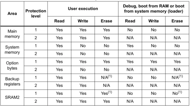
• Readout protection (RDP) to protect the whole memory. Three levels are available: – Level 0: no readout protection
– Level 1: memory readout protection: the Flash memory cannot be read from or written to if either debug features are connected, boot in RAM or bootloader is selected
– Level 2: chip readout protection: debug features (Cortex-M4 JTAG and serial wire), boot in RAM and bootloader selection are disabled (JTAG fuse). This selection is irreversible.
• Write protection (WRP): the protected area is protected against erasing and programming. Two areas can be selected, with 2-Kbyte granularity.
• Proprietary code readout protection (PCROP): a part of the flash memory can be protected against read and write from third parties. The protected area is execute-only: it can only be reached by the STM32 CPU, as an instruction code, while all other accesses (DMA, debug and CPU data read, write and erase) are strictly prohibited. The PCROP area granularity is 64-bit wide. An additional option bit (PCROP_RDP) allows to select if the PCROP area is erased or not when the RDP protection is changed from Level 1 to Level 0.
Table 3. Access status versus readout protection level and execution modes Area Protection level
User execution Debug, boot from RAM or boot from system memory (loader)
Read Write Erase Read Write Erase
Main memory
1 Yes Yes Yes No No No
2 Yes Yes Yes N/A N/A N/A
System memory
1 Yes No No Yes No No
2 Yes No No N/A N/A N/A
Option bytes
1 Yes Yes Yes Yes Yes Yes
2 Yes No No N/A N/A N/A
Backup registers
1 Yes Yes N/A(1)
1. Erased when RDP change from Level 1 to Level 0.
No No N/A(1)
2 Yes Yes N/A N/A N/A N/A
SRAM2 1 Yes Yes Yes
(1) No No No(1)
The whole non-volatile memory embeds the error correction code (ECC) feature supporting:
• single error detection and correction
• double error detection.
• The address of the ECC fail can be read in the ECC register
3.5 Embedded
SRAM
STM32L452xx devices feature 160 Kbyte of embedded SRAM. This SRAM is split into two blocks:
• 128 Kbyte mapped at address 0x2000 0000 (SRAM1)
• 32 Kbyte located at address 0x1000 0000 with hardware parity check (SRAM2). This memory is also mapped at address 0x2002 0000, offering a contiguous address space with the SRAM1 (32 Kbyte aliased by bit band)
This block is accessed through the ICode/DCode buses for maximum performance. These 32 Kbyte SRAM can also be retained in Standby mode.
The SRAM2 can be write-protected with 1 Kbyte granularity.
The memory can be accessed in read/write at CPU clock speed with 0 wait states.
3.6 Firewall
The device embeds a Firewall which protects code sensitive and secure data from any access performed by a code executed outside of the protected areas.
Each illegal access generates a reset which kills immediately the detected intrusion. The Firewall main features are the following:
• Three segments can be protected and defined thanks to the Firewall registers: – Code segment (located in Flash or SRAM1 if defined as executable protected
area)
– Non-volatile data segment (located in Flash) – Volatile data segment (located in SRAM1)
• The start address and the length of each segments are configurable: – Code segment: up to 1024 Kbyte with granularity of 256 bytes
– Non-volatile data segment: up to 1024 Kbyte with granularity of 256 bytes – Volatile data segment: up to 128 Kbyte with a granularity of 64 bytes
• Specific mechanism implemented to open the Firewall to get access to the protected areas (call gate entry sequence)
• Volatile data segment can be shared or not with the non-protected code
• Volatile data segment can be executed or not depending on the Firewall configuration The Flash readout protection must be set to level 2 in order to reach the expected level of protection.
3.7 Boot
modes
At startup, BOOT0 pin or nSWBOOT0 option bit, and BOOT1 option bit are used to select one of three boot options:
• Boot from user Flash
• Boot from system memory
• Boot from embedded SRAM
BOOT0 value may come from the PH3-BOOT0 pin or from an option bit depending on the value of a user option bit to free the GPIO pad if needed.
A Flash empty check mechanism is implemented to force the boot from system flash if the first flash memory location is not programmed and if the boot selection is configured to boot from main flash.
The boot loader is located in system memory. It is used to reprogram the Flash memory by using USART, I2C, SPI, CAN or USB FS in Device mode through DFU (device firmware upgrade).
3.8 Cyclic
redundancy
check calculation unit (CRC)
The CRC (cyclic redundancy check) calculation unit is used to get a CRC code using a configurable generator polynomial value and size.
Among other applications, CRC-based techniques are used to verify data transmission or storage integrity. In the scope of the EN/IEC 60335-1 standard, they offer a means of verifying the Flash memory integrity. The CRC calculation unit helps compute a signature of the software during runtime, to be compared with a reference signature generated at link-time and stored at a given memory location.
3.9 Power
supply
management
3.9.1
Power supply schemes
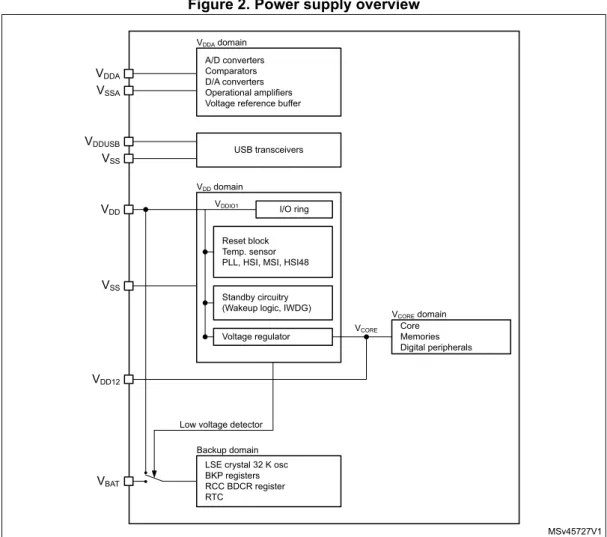
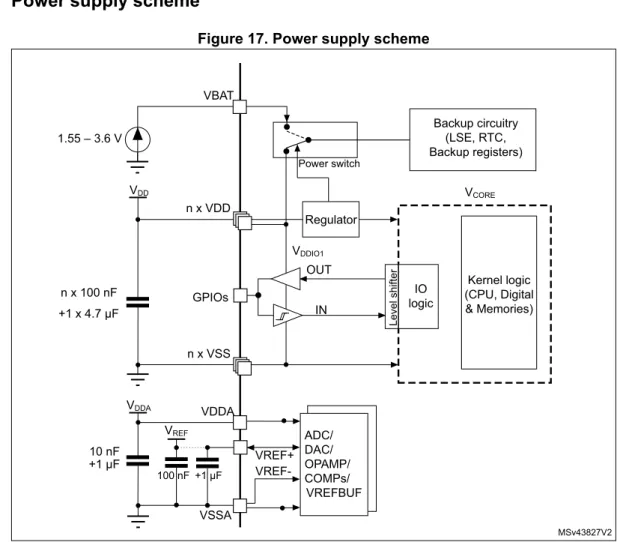
• VDD = 1.71 to 3.6 V: external power supply for I/Os (VDDIO1), the internal regulator and the system analog such as reset, power management and internal clocks. It is provided externally through VDD pins.
• VDD12 = 1.05 to 1.32 V: external power supply bypassing internal regulator when connected to an external SMPS. It is provided externally through VDD12 pins and only available on packages with the external SMPS supply option. VDD12 does not require any external decoupling capacitance and cannot support any external load.
• VDDA = 1.62 V (ADC/COMPs) / 1.8 (DAC/OPAMP) / 2.4 V (VREFBUF) to 3.6 V: external analog power supply for ADC, DAC, OPAMP, Comparators and Voltage reference buffer. The VDDA voltage level is independent from the VDD voltage.
• VDDUSB = 3.0 to 3.6 V: external independent power supply for USB transceivers. The VDDUSB voltage level is independent from the VDD voltage.
• VBAT = 1.55 to 3.6 V: power supply for RTC, external clock 32 kHz oscillator and backup registers (through power switch) when VDD is not present.
Note: When the functions supplied by VDDA are not used, this supply should preferably be shorted
Note: If these supplies are tied to ground, the I/Os supplied by these power supplies are not 5 V tolerant.
Note: VDDIOx is the I/Os general purpose digital functions supply. VDDIOx represents VDDIO1, with
VDDIO1 = VDD.
Figure 2. Power supply overview
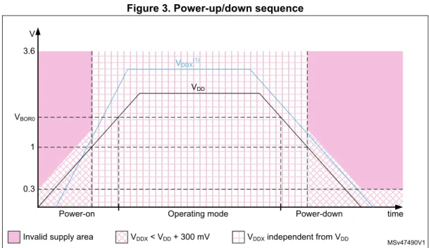
During power-up and power-down phases, the following power sequence requirements must be respected:
• When VDD is below 1 V, other power supplies (VDDA must remain below VDD + 300 mV.
• When VDD is above 1 V, all power supplies are independent.
During the power-down phase, VDD can temporarily become lower than other supplies only if the energy provided to the MCU remains below 1 mJ; this allows external decoupling capacitors to be discharged with different time constants during the power-down transient phase.
MSv45727V1 Low voltage detector
VDDA
VDDA domain
VSS VDD
VBAT
A/D converters Comparators D/A converters Operational amplifiers Voltage reference buffer
VDD domain
I/O ring VSSA
Reset block Temp. sensor PLL, HSI, MSI, HSI48
Standby circuitry (Wakeup logic, IWDG)
Voltage regulator VDDIO1
LSE crystal 32 K osc BKP registers RCC BDCR register RTC
Backup domain
Core Memories Digital peripherals VCORE domain VCORE
USB transceivers VDDUSB
VSS
Figure 3. Power-up/down sequence
1. VDDX refers to VDDA.
3.9.2
Power supply supervisor
The device has an integrated ultra-low-power brown-out reset (BOR) active in all modes except Shutdown and ensuring proper operation after power-on and during power down. The device remains in reset mode when the monitored supply voltage VDD is below a specified threshold, without the need for an external reset circuit.
The lowest BOR level is 1.71V at power on, and other higher thresholds can be selected through option bytes.The device features an embedded programmable voltage detector (PVD) that monitors the VDD power supply and compares it to the VPVD threshold. An interrupt can be generated when VDD drops below the VPVD threshold and/or when VDD is higher than the VPVD threshold. The interrupt service routine can then generate a warning message and/or put the MCU into a safe state. The PVD is enabled by software.
In addition, the device embeds a Peripheral Voltage Monitor which compares the independent supply voltage VDDA with a fixed threshold in order to ensure that the peripheral is in its functional supply range.
MSv47490V1 0.3
1 VBOR0 3.6
Operating mode
Power-on Power-down time
V
VDDX(1)
VDD
3.9.3 Voltage
regulator
Two embedded linear voltage regulators supply most of the digital circuitries: the main regulator (MR) and the low-power regulator (LPR).
• The MR is used in the Run and Sleep modes and in the Stop 0 mode.
• The LPR is used in Low-Power Run, Low-Power Sleep, Stop 1 and Stop 2 modes. It is also used to supply the 32 Kbyte SRAM2 in Standby with SRAM2 retention.
• Both regulators are in power-down in Standby and Shutdown modes: the regulator output is in high impedance, and the kernel circuitry is powered down thus inducing zero consumption.
The ultralow-power STM32L452xx supports dynamic voltage scaling to optimize its power consumption in run mode. The voltage from the Main Regulator that supplies the logic (VCORE) can be adjusted according to the system’s maximum operating frequency. There are two power consumption ranges:
• Range 1 with the CPU running at up to 80 MHz.
• Range 2 with a maximum CPU frequency of 26 MHz. All peripheral clocks are also limited to 26 MHz.
The VCORE can be supplied by the low-power regulator, the main regulator being switched off. The system is then in Low-power run mode.
• Low-power run mode with the CPU running at up to 2 MHz. Peripherals with independent clock can be clocked by HSI16.
When the MR is in use, the STM32L452xx with the external SMPS option allows to force an external VCORE supply on the VDD12 supply pins.
When VDD12 is forced by an external source and is higher than the output of the internal LDO, the current is taken from this external supply and the overall power efficiency is significantly improved if using an external step down DC/DC converter.
3.9.4 Low-power
modes
The ultra-low-power STM32L452xx supports seven low-power modes to achieve the best compromise between low-power consumption, short startup time, available peripherals and available wakeup sources.
tiona l ov erv ie w STM3 2L4 15 DS1 19
12 Rev 5
Table 4. STM32L452xx modes overview
Mode Regulator(1) CPU Flash SRAM Clocks DMA & Peripherals(2) Wakeup source Consumption(3) Wakeup time
Run
MR range 1
Yes ON(6) ON Any
All
N/A
94µA/MHz
N/A SMPS range 2 High 34µA/MHz(4)
MR range2
All except USB_FS, RNG 85 µA/MHz SMPS range 2 Low 37µA/MHz(5)
LPRun LPR Yes ON(6) ON
Any except
PLL
All except USB_FS, RNG N/A 95 µA/MHz to Range 1: 4 µs to Range 2: 64 µs
Sleep
MR range 1
No ON(6) ON(7) Any
All
Any interrupt or event
27 µA/MHz
6 cycles SMPS range 2 High 10 µA/MHz(4)
MR range2
All except USB_FS, RNG 27 µA/MHz SMPS range 2 Low 11 µA/MHz(5)
LPSleep LPR No ON(6) ON(7) Any except
PLL
All except USB_FS, RNG Any interrupt or event 38 µA/MHz 6 cycles
Stop 0
MR Range 1(8)
No OFF ON LSE LSI
BOR, PVD, PVM RTC, IWDG COMPx (x=1,2)
DAC1 OPAMPx (x=1) USARTx (x=1...3)(9)
UART4(9) LPUART1(9) I2Cx (x=1...4)(10)
LPTIMx (x=1,2) ***
All other peripherals are
Reset pin, all I/Os BOR, PVD, PVM
RTC, IWDG COMPx (x=1..2) USARTx (x=1...3)(9)
UART4(9) LPUART1(9) I2Cx (x=1...4)(10)
LPTIMx (x=1,2) USB_FS(11)
125 µA
2.47 µs in SRAM 4.1 µs in Flash
L
45
2x
x
Func
tiona
l ov
DS1
19
12 Rev 5
Stop 1 LPR No Off ON LSE LSI
BOR, PVD, PVM RTC, IWDG COMPx (x=1,2)
DAC1 OPAMPx (x=1) USARTx (x=1...3)(9)
UART4(9) LPUART1(9) I2Cx (x=1...4)(10)
LPTIMx (x=1,2) ***
All other peripherals are frozen.
Reset pin, all I/Os BOR, PVD, PVM
RTC, IWDG COMPx (x=1..2) USARTx (x=1...3)(9)
UART4(9) LPUART1(9) I2Cx (x=1...4)(10)
LPTIMx (x=1,2) USB_FS(11)
9.85 µA w/o RTC 10.5 µA w RTC
5.7 µs in SRAM 7 µs in Flash
Stop 2 LPR No Off ON LSE LSI
BOR, PVD, PVM RTC, IWDG COMPx (x=1..2)
I2C3(10) LPUART1(9)
LPTIM1 ***
All other peripherals are frozen.
Reset pin, all I/Os BOR, PVD, PVM
RTC, IWDG COMPx (x=1..2)
I2C3(10) LPUART1(9)
LPTIM1
2.05 µA w/o RTC 2.30 µA w/RTC
5.8 µs in SRAM 8.3 µs in Flash
tiona
l ov
erv
ie
w
STM3
2L4
15
DS1
19
12 Rev 5
Standby
LPR
Power ed Off Off
SRAM 2 ON
LSE LSI
BOR, RTC, IWDG ***
All other peripherals are powered off.
***
I/O configuration can be floating, pull-up or pull-down
Reset pin 5 I/Os (WKUPx)(12)
BOR, RTC, IWDG
0.35 µA w/o RTC 0.52 µA w/ RTC
16.1 µs OFF
Power ed Off
0.10 µA w/o RTC 0.27 µA w/ RTC
Shutdown OFF Power ed Off Off
Power ed Off
LSE
RTC ***
All other peripherals are powered off.
***
I/O configuration can be floating, up or
pull-down(13)
Reset pin 5 I/Os (WKUPx)(12)
RTC
0.02 µA w/o RTC
0.17 µA w/ RTC 256 µs
1. LPR means Main regulator is OFF and Low-power regulator is ON. 2. All peripherals can be active or clock gated to save power consumption.
3. Typical current at VDD = 1.8 V, 25°C. Consumptions values provided running from SRAM, Flash memory Off, 80 MHz in Range 1, 26 MHz in Range 2, 2 MHz in LPRun/LPSleep.
4. Theoretical value based on VDD = 3.3 V, DC/DC Efficiency of 85%, VCORE = 1.10 V 5. Theoretical value based on VDD = 3.3 V, DC/DC Efficiency of 85%, VCORE = 1.05 V
6. The Flash memory can be put in power-down and its clock can be gated off when executing from SRAM. 7. The SRAM1 and SRAM2 clocks can be gated on or off independently.
8. SMPS mode can be used in STOP0 Mode, but no significant power gain can be expected.
9. U(S)ART and LPUART reception is functional in Stop mode, and generates a wakeup interrupt on Start, address match or received frame event. 10. I2C address detection is functional in Stop mode, and generates a wakeup interrupt in case of address match.
11. USB_FS wakeup by resume from suspend and attach detection protocol event.
12. The I/Os with wakeup from Standby/Shutdown capability are: PA0, PC13, PE6, PA2, PC5.
13. I/Os can be configured with internal pull-up, pull-down or floating in Shutdown mode but the configuration is lost when exiting the Shutdown mode.
By default, the microcontroller is in Run mode after a system or a power Reset. It is up to the user to select one of the low-power modes described below:
• Sleep mode
In Sleep mode, only the CPU is stopped. All peripherals continue to operate and can wake up the CPU when an interrupt/event occurs.
• Low-power run mode
This mode is achieved with VCORE supplied by the low-power regulator to minimize the regulator's operating current. The code can be executed from SRAM or from Flash, and the CPU frequency is limited to 2 MHz. The peripherals with independent clock can be clocked by HSI16.
• Low-power sleep mode
This mode is entered from the low-power run mode. Only the CPU clock is stopped. When wakeup is triggered by an event or an interrupt, the system reverts to the low-power run mode.
• Stop 0, Stop 1 and Stop 2 modes
Stop mode achieves the lowest power consumption while retaining the content of SRAM and registers. All clocks in the VCORE domain are stopped, the PLL, the MSI RC, the HSI16 RC and the HSE crystal oscillators are disabled. The LSE or LSI is still running.
The RTC can remain active (Stop mode with RTC, Stop mode without RTC).
Some peripherals with wakeup capability can enable the HSI16 RC during Stop mode to detect their wakeup condition.
Three Stop modes are available: Stop 0, Stop 1 and Stop 2 modes. In Stop 2 mode, most of the VCORE domain is put in a lower leakage mode.
Stop 1 offers the largest number of active peripherals and wakeup sources, a smaller wakeup time but a higher consumption than Stop 2. In Stop 0 mode, the main regulator remains ON, allowing a very fast wakeup time but with much higher consumption. The system clock when exiting from Stop 0, Stop 1 or Stop 2 modes can be either MSI up to 48 MHz or HSI16, depending on software configuration.
• Standby mode
The Standby mode is used to achieve the lowest power consumption with BOR. The internal regulator is switched off so that the VCORE domain is powered off. The PLL, the MSI RC, the HSI16 RC and the HSE crystal oscillators are also switched off.
The RTC can remain active (Standby mode with RTC, Standby mode without RTC). The brown-out reset (BOR) always remains active in Standby mode.
The state of each I/O during standby mode can be selected by software: I/O with internal pull-up, internal pull-down or floating.
After entering Standby mode, SRAM1 and register contents are lost except for registers in the Backup domain and Standby circuitry. Optionally, SRAM2 can be retained in Standby mode, supplied by the low-power Regulator (Standby with SRAM2 retention mode).
The device exits Standby mode when an external reset (NRST pin), an IWDG reset, WKUP pin event (configurable rising or falling edge), or an RTC event occurs (alarm, periodic wakeup, timestamp, tamper) or a failure is detected on LSE (CSS on LSE). The system clock after wakeup is MSI up to 8 MHz.
• Shutdown mode
The Shutdown mode allows to achieve the lowest power consumption. The internal regulator is switched off so that the VCORE domain is powered off. The PLL, the HSI16, the MSI, the LSI and the HSE oscillators are also switched off.
The RTC can remain active (Shutdown mode with RTC, Shutdown mode without RTC). The BOR is not available in Shutdown mode. No power voltage monitoring is possible in this mode, therefore the switch to Backup domain is not supported.
SRAM1, SRAM2 and register contents are lost except for registers in the Backup domain.
The device exits Shutdown mode when an external reset (NRST pin), a WKUP pin event (configurable rising or falling edge), or an RTC event occurs (alarm, periodic wakeup, timestamp, tamper).
Table 5. Functionalities depending on the working mode(1)
Peripheral Run Sleep
Low-power run Low-power sleep
Stop 0/1 Stop 2 Standby Shutdown
VBAT -W ak eup cap ab ility -W ak eup cap ab ility -W ak eup cap ab ility -W ak eup cap ab ility
CPU Y - Y - - -
-Flash memory (up to
512 KB) O(2) O(2) O(2) O(2) - - -
-SRAM1 (128 KB) Y Y(3) Y Y(3) Y - Y - - -
-SRAM2 (32 KB) Y Y(3) Y Y(3) Y - Y - O(4) - - -
-Quad SPI O O O O - - -
-Backup Registers Y Y Y Y Y - Y - Y - Y - Y
Brown-out reset
(BOR) Y Y Y Y Y Y Y Y Y Y - -
-Programmable Voltage Detector (PVD)
O O O O O O O O - - - -
-Peripheral Voltage Monitor (PVMx; x=1,3,4)
O O O O O O O O - - - -
-DMA O O O O - - -
-High Speed Internal
(HSI16) O O O O (5) - (5) - - -
-Oscillator RC48 O O - - -
-High Speed External
(HSE) O O O O - - -
-Low Speed Internal
(LSI) O O O O O - O - O - - -
-Low Speed External
(LSE) O O O O O - O - O - O - O
Multi-Speed Internal
(MSI) O O O O - - -
-Clock Security
System (CSS) O O O O - - -
-Clock Security
System on LSE O O O O O O O O O O - -
-RTC / Auto wakeup O O O O O O O O O O O O O
Number of RTC
USARTx (x=1,2,3)
UART4 O O O O O(6) O(6) - - -
-Low-power UART
(LPUART) O O O O O(6) O(6) O(6) O(6) - - - -
-I2Cx (x=1,2,4) O O O O O(7) O(7) - - -
-I2C3 O O O O O(7) O(7) O(7) O(7) - - - -
-SPIx (x=1,2,3) O O O O - - -
-CAN O O O O - - -
-SDMMC1 O O O O - - -
-SAIx (x=1) O O O O - - -
-DFSDM1 O O O O - - -
-ADCx (x=1) O O O O - - -
-DAC1 O O O O O - - -
-VREFBUF O O O O O - - -
-OPAMPx (x=1) O O O O O - - -
-COMPx (x=1,2) O O O O O O O O - - - -
-Temperature sensor O O O O - - -
-Timers (TIMx) O O O O - - -
-Low-power timer 1
(LPTIM1) O O O O O O O O - - - -
-Low-power timer 2
(LPTIM2) O O O O O O - - -
-Independent
watchdog (IWDG) O O O O O O O O O O - -
-Window watchdog
(WWDG) O O O O - - -
-SysTick timer O O O O - - -
-Touch sensing
controller (TSC) O O O O - - -
-Random number
generator (RNG) O(8) O(8) - - -
-Table 5. Functionalities depending on the working mode(1) (continued)
Peripheral Run Sleep
Low-power
run
Low-power
sleep
Stop 0/1 Stop 2 Standby Shutdown
VBAT
-W
a
keu
p ca
pab
ility
-W
a
keu
p ca
pab
ility
-W
a
keu
p ca
pab
ility
-W
a
keu
p ca
pab
3.9.5 Reset
mode
In order to improve the consumption under reset, the I/Os state under and after reset is “analog state” (the I/O schmitt trigger is disable). In addition, the internal reset pull-up is deactivated when the reset source is internal.
3.9.6 VBAT
operation
The VBAT pin allows to power the device VBAT domain from an external battery, an external supercapacitor, or from VDD when no external battery and an external supercapacitor are present. The VBAT pin supplies the RTC with LSE and the backup registers. Three anti-tamper detection pins are available in VBAT mode.
VBAT operation is automatically activated when VDD is not present.
An internal VBAT battery charging circuit is embedded and can be activated when VDD is present.
Note: When the microcontroller is supplied from VBAT, external interrupts and RTC alarm/events
do not exit it from VBAT operation.
CRC calculation unit O O O O - - -
-GPIOs O O O O O O O O (9) pins5
(10)
(11) pins5 (10)
-1. Legend: Y = Yes (Enable). O = Optional (Disable by default. Can be enabled by software). - = Not available. 2. The Flash can be configured in power-down mode. By default, it is not in power-down mode.
3. The SRAM clock can be gated on or off.
4. SRAM2 content is preserved when the bit RRS is set in PWR_CR3 register.
5. Some peripherals with wakeup from Stop capability can request HSI16 to be enabled. In this case, HSI16 is woken up by the peripheral, and only feeds the peripheral which requested it. HSI16 is automatically put off when the peripheral does not need it anymore.
6. UART and LPUART reception is functional in Stop mode, and generates a wakeup interrupt on Start, address match or received frame event.
7. I2C address detection is functional in Stop mode, and generates a wakeup interrupt in case of address match. 8. Voltage scaling Range 1 only.
9. I/Os can be configured with internal pull-up, pull-down or floating in Standby mode. 10. The I/Os with wakeup from Standby/Shutdown capability are: PA0, PC13, PE6, PA2, PC5.
11. I/Os can be configured with internal pull-up, pull-down or floating in Shutdown mode but the configuration is lost when exiting the Shutdown mode.
Table 5. Functionalities depending on the working mode(1) (continued)
Peripheral Run Sleep
Low-power
run
Low-power
sleep
Stop 0/1 Stop 2 Standby Shutdown
VBAT
-W
a
keu
p ca
pab
ility
-W
a
keu
p ca
pab
ility
-W
a
keu
p ca
pab
ility
-W
a
keu
p ca
pab
3.10 Interconnect
matrix
Several peripherals have direct connections between them. This allows autonomous communication between peripherals, saving CPU resources thus power supply
consumption. In addition, these hardware connections allow fast and predictable latency. Depending on peripherals, these interconnections can operate in Run, Sleep, low-power run and sleep, Stop 0, Stop 1 and Stop 2 modes.
Table 6. STM32L452xx peripherals interconnect matrix
Interconnect source Interconnect destination Interconnect action
Run Sleep
Lo
w-p
o
w
er ru
n
Lo
w-p
o
w
e
r sl
ee
p
St
op 0 /
Stop 1
Stop 2
TIMx
TIMx Timers synchronization or chaining Y Y Y Y - -ADCx
DAC1 DFSDM1
Conversion triggers Y Y Y Y -
-DMA Memory to memory transfer trigger Y Y Y Y -
-COMPx Comparator output blanking Y Y Y Y -
-TIM15/TIM16 IRTIM Infrared interface output generation Y Y Y Y -
-COMPx
TIM1 TIM2
Timer input channel, trigger, break from
analog signals comparison Y Y Y Y -
-LPTIMERx Low-power timer triggered by analog signals comparison Y Y Y Y Y (1)Y
ADCx TIM1 Timer triggered by analog watchdog Y Y Y Y -
-RTC
TIM16 Timer input channel from RTC events Y Y Y Y - -LPTIMERx Low-power timer triggered by RTC alarms or tampers Y Y Y Y Y (1)Y All clocks sources (internal
and external)
TIM2 TIM15, 16
Clock source used as input channel for
RC measurement and trimming Y Y Y Y -
-CSS
CPU (hard fault) RAM (parity error)
Flash memory (ECC error) COMPx
PVD
DFSDM1 (analog watchdog, short circuit detection)
TIM1
-GPIO
TIMx External trigger Y Y Y Y -
-LPTIMERx External trigger Y Y Y Y Y (1)Y
ADCx DAC1 DFSDM1
Conversion external trigger Y Y Y Y -
-1. LPTIM1 only.
Table 6. STM32L452xx peripherals interconnect matrix (continued)
Interconnect source Interconnect destination Interconnect action
Run Sleep
Low
-p
owe
r run
Lo
w-p
o
wer sleep
Stop 0
/ Stop
1
3.11
Clocks and startup
The clock controller (see Figure 4) distributes the clocks coming from different oscillators to the core and the peripherals. It also manages clock gating for low-power modes and ensures clock robustness. It features:
• Clock prescaler: to get the best trade-off between speed and current consumption, the clock frequency to the CPU and peripherals can be adjusted by a programmable prescaler
• Safe clock switching: clock sources can be changed safely on the fly in run mode through a configuration register.
• Clock management: to reduce power consumption, the clock controller can stop the clock to the core, individual peripherals or memory.
• System clock source: four different clock sources can be used to drive the master clock SYSCLK:
– 4-48 MHz high-speed external crystal or ceramic resonator (HSE), that can supply a PLL. The HSE can also be configured in bypass mode for an external clock. – 16 MHz high-speed internal RC oscillator (HSI16), trimmable by software, that can
supply a PLL
– Multispeed internal RC oscillator (MSI), trimmable by software, able to generate 12 frequencies from 100 kHz to 48 MHz. When a 32.768 kHz clock source is available in the system (LSE), the MSI frequency can be automatically trimmed by hardware to reach better than ±0.25% accuracy. The MSI can supply a PLL. – System PLL which can be fed by HSE, HSI16 or MSI, with a maximum frequency
at 80 MHz.
• RC48 with clock recovery system (HSI48): internal RC48 MHz clock source can be used to drive the SDMMC or the RNG peripherals. This clock can be output on the MCO.
• Auxiliary clock source: two ultralow-power clock sources that can be used to drive the real-time clock:
– 32.768 kHz low-speed external crystal (LSE), supporting four drive capability modes. The LSE can also be configured in bypass mode for an external clock. – 32 kHz low-speed internal RC (LSI), also used to drive the independent watchdog.
The LSI clock accuracy is ±5% accuracy.
• Peripheral clock sources: Several peripherals (SDMMC, RNG, SAI, USARTs, I2Cs, LPTimers, ADC) have their own independent clock whatever the system clock. Two PLLs, each having three independent outputs allowing the highest flexibility, can generate independent clocks for the ADC, the SDMMC/RNG and the SAI.
• Startup clock: after reset, the microcontroller restarts by default with an internal 4 MHz clock (MSI). The prescaler ratio and clock source can be changed by the application program as soon as the code execution starts.
• Clock security system (CSS): this feature can be enabled by software. If a HSE clock failure occurs, the master clock is automatically switched to HSI16 and a software
interrupt is generated if enabled. LSE failure can also be detected and generated an interrupt.
• Clock-out capability:
– MCO: microcontroller clock output: it outputs one of the internal clocks for external use by the application. Low frequency clocks (LSI, LSE) are available down to Stop 1 low power state.
– LSCO: low speed clock output: it outputs LSI or LSE in all low-power modes down to Standby mode. LSE can also be output on LSCO in Shutdown mode. LSCO is not available in VBAT mode.
Several prescalers allow to configure the AHB frequency, the high speed APB (APB2) and the low speed APB (APB1) domains. The maximum frequency of the AHB and the APB domains is 80 MHz.
Figure 4. Clock tree MSv40980V2 SYSCLK MCO LSCO PLL to IWDG to RTC to PWR HCLK
to AHB bus, core, memory and DMA
FCLK Cortex free running clock
to Cortex system timer
to APB1 peripherals
to APB2 peripherals
PCLK1
PCLK2
LSE HSI16
SYSCLK to USARTx
x=2..3 to UART4 to LPUART1 to I2Cx x=1,2,3,4 to LPTIMx x=1,2 SAI1_EXTCLK to TIMx x=2,6,7 OSC32_OUT OSC32_IN MSI HSI16 HSE HSI16 LSI LSE HSE SYSCLK HSE MSI HSI16 LSE OSC
32.768 kHz /32
AHB PRESC / 1,2,..512
/ 8 APB1 PRESC
/ 1,2,4,8,16
x1 or x2
HSI16 SYSCLK LSI LSE HSI16 APB2 PRESC / 1,2,4,8,16 to TIMx x=1,15,16 x1 or x2
to USART1 LSE HSI16 SYSCLK / P / Q / R PLLSAI1 / P / Q / R / M MSI RC
100 kHz – 48 MHz HSI RC 16 MHz HSE OSC 4-48 MHz Clock detector OSC_OUT OSC_IN / 1→16 LSI RC 32 kHz
Clock source control PLLSAI1CLK PLL48M1CLK PLLCLK PLLSAI2CLK PLL48M2CLK PLLADC1CLK HSI48 MSI PLLCLK
48 MHz clock to USB, RNG, SDMMC to ADC to SAI1 MSI SYSCLK PLLADC1CLK HSI16 HSI16 HSI RC 48 MHz CRS
3.12 General-purpose
inputs/outputs (GPIOs)
Each of the GPIO pins can be configured by software as output (push-pull or open-drain), as input (with or without pull-up or pull-down) or as peripheral alternate function. Most of the GPIO pins are shared with digital or analog alternate functions. Fast I/O toggling can be achieved thanks to their mapping on the AHB2 bus.
The I/Os alternate function configuration can be locked if needed following a specific sequence in order to avoid spurious writing to the I/Os registers.
3.13
Direct memory access controller (DMA)
The device embeds 2 DMAs. Refer to Table 7: DMA implementation for the features implementation.
Direct memory access (DMA) is used in order to provide high-speed data transfer between peripherals and memory as well as memory to memory. Data can be quickly moved by DMA without any CPU actions. This keeps CPU resources free for other operations.
The two DMA controllers have 14 channels in total, each dedicated to managing memory access requests from one or more peripherals. Each has an arbiter for handling the priority between DMA requests.
The DMA supports:
• 14 independently configurable channels (requests)
• Each channel is connected to dedicated hardware DMA requests, software trigger is also supported on each channel. This configuration is done by software.
• Priorities between requests from channels of one DMA are software programmable (4 levels consisting of very high, high, medium, low) or hardware in case of equality (request 1 has priority over request 2, etc.)
• Independent source and destination transfer size (byte, half word, word), emulating packing and unpacking. Source/destination addresses must be aligned on the data size.
• Support for circular buffer management
• 3 event flags (DMA Half Transfer, DMA Transfer complete and DMA Transfer Error) logically ORed together in a single interrupt request for each channel
• Memory-to-memory transfer
• Peripheral-to-memory and memory-to-peripheral, and peripheral-to-peripheral transfers
• Access to Flash, SRAM, APB and AHB peripherals as source and destination
• Programmable number of data to be transferred: up to 65536.
Table 7. DMA implementation
DMA features DMA1 DMA2
3.14 Interrupts
and
events
3.14.1
Nested vectored interrupt controller (NVIC)
The devices embed a nested vectored interrupt controller able to manage 16 priority levels, and handle up to 67 maskable interrupt channels plus the 16 interrupt lines of the Cortex® -M4.
The NVIC benefits are the following:
• Closely coupled NVIC gives low latency interrupt processing
• Interrupt entry vector table address passed directly to the core
• Allows early processing of interrupts
• Processing of late arriving higher priority interrupts
• Support for tail chaining
• Processor state automatically saved on interrupt entry, and restored on interrupt exit, with no instruction overhead
The NVIC hardware block provides flexible interrupt management features with minimal interrupt latency.
3.14.2
Extended interrupt/event controller (EXTI)
The extended interrupt/event controller consists of 37 edge detector lines used to generate interrupt/event requests and wake-up the system from Stop mode. Each external line can be independently configured to select the trigger event (rising edge, falling edge, both) and can be masked independently. A pending register maintains the status of the interrupt requests. The internal lines are connected to peripherals with wakeup from Stop mode capability. The EXTI can detect an external line with a pulse width shorter than the internal clock period. Up to 83 GPIOs can be connected to the 16 external interrupt lines.