Features
D
Qualified for Automotive Applications
D
Wide Range of Digital and Analog Signal
Levels
− Digital: 3 V to 20 V
− Analog:
3
20 V
P-PD
Low ON Resistance, 125
Ω
(Typ) Over
15 V
P-PSignal Input Range
for V
DD− V
EE= 18 V
D
High OFF Resistance, Channel Leakage of
+
100 pA (Typ) at V
DD− V
EE= 18 V
D
Logic-Level Conversion for Digital
Addressing Signals of 3 V to 20 V
(V
DD− V
SS= 3 V to 20 V) to Switch Analog
Signals to 20 V
P-P(V
DD− V
EE= 20 V)
D
Matched Switching Characteristics,
r
on= 5
Ω
(Typ) for V
DD− V
EE= 15 V
D
Very Low Quiescent Power Dissipation
Under All Digital-Control Input and Supply
Conditions, 0.2
µ
W (Typ)
at V
DD− V
SS= V
DD− V
EE= 10 V
D
Binary Address Decoding on Chip
D
5-V, 10-V, and 15-V Parametric Ratings
D
100% Tested for Quiescent Current at 20 V
D
Maximum Input Current of 1
µ
A at 18 V Over
Full Package Temperature Range, 100 nA at
18 V and 25
°
C
D
Break-Before-Make Switching Eliminates
Channel Overlap
Applications
D
Analog and Digital Multiplexing and
Demultiplexing
D
Analog-to-Digital (A/D) and
Digital-to-Analog (D/A) Conversion
D
Signal Gating
description/ordering information
The CD4051B, CD4052B, and CD4053B analog multiplexers are digitally-controlled analog switches that have
low ON impedance and very low OFF leakage current. Control of analog signals up to 20 V
P-Pcan be achieved
by digital signal amplitudes of 4.5 V to 20 V (If V
DD− V
SS= 3 V, a V
DD− V
EEof up to 13 V can be controlled;
for V
DD− V
EElevel differences above 13 V, a V
DD− V
SSof at least 4.5 V is required). For example, if
V
DD= 4.5 V, V
SS= 0 V, and V
EE= −13.5 V, analog signals from −13.5 V to 4.5 V can be controlled by digital
inputs of 0 V to 5 V. These multiplexer circuits dissipate extremely low quiescent power over the full V
DD− V
SSand V
DD− V
EEsupply-voltage ranges, independent of the logic state of the control signals. When a logic high
(H) is present at the inhibit (INH) input, all channels are off.
ORDERING INFORMATION
† TA PACKAGE‡ ORDERABLE PART NUMBER TOP-SIDE MARKING SOIC − M Reel of 2500 CD4051BQM96Q1 CD4051Q TSSOP − PW Reel of 2000 CD4051BQPWRQ1 CM051BQ 40°C to 125°C SOIC − M Reel of 2500 CD4052BQM96Q1§ CD4052Q −40°C to 125°C TSSOP − PW Reel of 2000 CD4052BQPWRQ1§ CD4052Q SOIC − M Reel of 2500 CD4053BQM96Q1 CD4053Q TSSOP − PW Reel of 2000 CD4053BQPWRQ1§ CD4053Qdescription/ordering information (continued)
The CD4051B is a single eight-channel multiplexer that has three binary control inputs (A, B, and C) and an
inhibit input. The three binary signals select one of eight channels to be turned on and connect one of the eight
inputs to the output.
The CD4052B is a differential four-channel multiplexer that has two binary control inputs (A and B) and an inhibit
input. The two binary input signals select one of four pairs of channels to be turned on and connect the analog
inputs to the outputs.
The CD4053B is a triple two-channel multiplexer with three separate digital control inputs (A, B, and C) and an
inhibit input. Each control input selects one of a pair of channels, which are connected in a single-pole,
double-throw configuration.
When these devices are used as demultiplexers, the CHANNEL IN/OUT terminals are the outputs, and the
common (COM OUT/IN) terminals are the inputs.
CD4053 M OR PW PACKAGE (TOP VIEW) 1 2 3 4 5 6 7 8 16 15 14 13 12 11 10 9 IN/OUT by IN/OUT bx IN/OUT cy OUT/IN CX OR CY IN/OUT CX INH VEE VSS VDD OUT/IN bx or by OUT/IN ax or ay IN/OUT ay IN/OUT ax A B C CD4051 M OR PW PACKAGE (TOP VIEW) 1 2 3 4 5 6 7 8 16 15 14 13 12 11 10 9 CHANNEL I/O 4 CHANNEL I/O 6 COM OUT/IN CHANNEL I/O 7 CHANNEL I/O 5 INH VEE VSS VDD CHANNEL I/O 2 CHANNEL I/O 1 CHANNEL I/O 0 CHANNEL I/O 3 A B C CD4052 M OR PW PACKAGE (TOP VIEW) 1 2 3 4 5 6 7 8 16 15 14 13 12 11 10 9 Y CHANNEL I/O 0 Y CHANNEL I/O 2 COM Y OUT/IN Y CHANNEL I/O 3 Y CHANNEL I/O 1 INH VEE VSS VDD X CHANNEL I/O 2 X CHANNEL I/O 1 COM X OUT/IN X CHANNEL I/O 0 X CHANNEL I/O 3 A B
Function Tables
CD4051 INPUTS ON INH C B A ON CHANNEL L L L L 0 L L L H 1 L L H L 2 L L H H 3 L H L L 4 L H L H 5 L H H L 6 L H H H 7 H X X X None X = don’t care CD4052 INPUTS ON INH B A ON CHANNEL L L L 0x, 0y L L H 1x, 2y L H L 2x, 2y L H H 3x, 3y H X X None X = don’t care CD4053 INPUTS ON INH A OR B OR C ON CHANNEL L L ax or bx or cx L H ay or by or cy H X None X = don’t carelogic diagram (positive logic)
†All inputs are protected by CMOS protection network.
11 10 9 6 A B C INH 13 4 2 5 1 12 15 14 TG TG TG TG TG TG TG TG 3 COM OUT/IN 0 1 2 3 4 5 6 7 8 7 16 CHANNEL I/O † † † † CD4051B Logic-Level Conversion Binary to 1-of-8 Decoder With Inhibit VDD VSS VEE CD4052B 12 11 15 14 0 1 2 3 X CHANNEL I/O 13 3 16 6 9 10 A B INH TG TG TG TG TG TG Binary to 1-of-4 Decoder With † † † COM X OUT/IN Logic-Level Conversion VDD COM Y OUT/IN
logic diagrams (positive logic) (continued)
11 10 9 6 A† B† C† INH† 12 3 5 1 2 13 TG TG TG TG TG TG 4 ax ay bx by cx cy 8 7 16 IN/OUT 15 14 VDD†All inputs are protected by standard CMOS protection network.
CD4053B Logic-Level Conversion VDD VSS VEE Binary to 1-of-2 Decoders With Inhibit COM OUT/IN ac or ay COM OUT/IN bc or by COM OUT/IN xc or xy
absolute maximum ratings over operating free-air temperature (unless otherwise noted)
‡Supply voltage range, V+ to V− (voltages referenced to V
SSterminal)
. . .
−0.5 to 20 V
DC input voltage range
. . .
−0.5 V to V
DD+ 0.5 V
DC input current, any one input
. . .
±
10 mA
Package thermal impedance,
θ
JA(see Note 1): M package
. . .
73
°
C/W
PW package
. . .
108
°
C/W
Maximum junction temperature, T
J150
. . .
°
C
Lead temperature (during soldering):
At distance 1/16
±
1/32 inch (1,59
±
0,79 mm) from case for 10 s max
. . .
265
°
C
Storage temperature range, T
stg−65
. . .
°
C to 150
°
C
recommended operating conditions
MIN MAX UNIT
V Supply voltage 5 20 V
VDD Supply voltage 5 20 V
TA Operating free-air temperature −40 125 °C
electrical characteristics, V
SUPPLY=
±
5 V, A
V= 1 V, R
L= 100
Ω
, unless otherwise noted
(see Note 2)
PARAMETER TEST CONDITIONS VDD
LIMITS AT INDICATED TEMPERATURES
UNIT
PARAMETER TEST CONDITIONS VDD
(V)
40°C 125°C
25°C UNIT
(V)
−40°C 125°C
MIN TYP MAX
5 5 150 0.04 5 I Quiescent device 10 10 300 0.04 10 A IDD Quiescent device current 15 20 600 0.04 20 µA 20 100 3000 0.08 100
Signal Input (Vis) and Output (Vos)
D i t V 0 V V 0 V 5 850 1300 470 1050 ron Drain-to-source ON-state resistance VEE = 0 V, VSS = 0 V, VIS= 0 to VDD 10 330 550 180 400 Ω ron ON-state resistance VIS = 0 to VDD 15 210 320 125 240 Ω ON-state resistance 5 15 ∆ron ON-state resistance difference between VEE = 0 V, VSS = 0 V 10 10 Ω ∆ron difference between
any two switches
VEE 0 V, VSS 0 V
15 5
Ω
Input/output leakage current (switch off)
Any channel OFF (MAX) or all channels OFF (COM OUT/IN) (Max),
VEE = 0 V, VSS = 0 V, See Note 3 18 ±0.1 ±1 ±10−5 ±0.1 µA Cis Input capacitance VEE = −5 V, VSS = −5 V 5 5 pF CD4051 30 Cos Output capacitance VEE = −5 V, VSS = −5 V CD4052 5 18 pF Cos Output capacitance VEE 5 V, VSS 5 V CD4053 5 9 pF
Cios Feedthroughcapacitance VEE = −5 V, VSS = −5 V 5 0.2 pF
Propagation delay
V V R 200 kΩ
5 30 60
tpd
Propagation delay
(signal input to VIS(p-p) = VDD, RL = 200 kΩ,
CL= 50 pF tr tf= 20 ns 10 15 30 ns
tpd (signal input to
output) CL = 50 pF, tr, tf = 20 ns 15 10 20
ns
NOTES: 2. Peak-to-peak voltage symmetrical about VDD − VEE
2
electrical characteristics, V
SUPPLY=
±
5 V, A
V= 1 V, R
L= 100
Ω
, unless otherwise noted
(see Note 2) (continued)
PARAMETER TEST CONDITIONS VEE VDD
LIMITS AT INDICATED TEMPERATURES
UNIT
PARAMETER TEST CONDITIONS VEE
(V) VDD (V) 40°C 125°C 25°C UNIT (V) (V) −40°C 125°C
MIN TYP MAX
Control (Address or Inhibit), VC
VIL = VDD through 1kΩ, VSS 5 1.5 1.5 1.5
VIL Input low voltage
IL DD g ,
VIH = VDD through 1kΩ,
RL= 1kΩto VSS VSS 10 3 3 3 V
IL p g R
L = 1kΩ to VSS,
Iis < 2 µA on all OFF channels VSS 15 4 4 4
VIL = VDD through 1kΩ, VSS 5 3.5 3.5 3.5
VIH Input high voltage
IL DD g , VIH = VDD through 1kΩ, RL= 1kΩto VSS VSS 10 7 7 7 V IH p g g R L = 1kΩ to VSS,
Iis < 2 µA on all OFF channels VSS 15 11 11 11
IIN Input current VIN = 0 V, 18 V 18 ±0.1 ±1 ±10−5 ±0.1 µA Address-to-signal t tf= 20 ns CL= 50 pF 0 5 450 720 t Address-to-signal OUT (channels ON tr, tf = 20 ns, CL = 50 pF, RL = 10 kΩ, VSS = 0 V, 0 10 160 320 ns tpd1 OUT (channels ON or OFF) propagation d l RL = 10 kΩ, VSS = 0 V,
See Figure 10, Figure 11, and Fi 14 0 15 120 240 ns ) p p g delay g g Figure 14 −5 5 225 450 Inhibit-to-signal 0 5 400 720 t Inhibit-to-signal OUT (channel tr, tf = 20 ns, CL = 50 pF, R 1 kΩ V 0 V 0 10 160 320 ns tpd2 OUT (channel turning ON) ti d l RL = 1 kΩ, VSS = 0 V, See Figure 11 0 15 120 240 ns g )
propagation delay See Figure 11
−10 5 200 400 Inhibit-to-signal 0 5 200 450 t Inhibit-to-signal OUT (channel tr, tf = 20 ns, CL = 50 pF, R 10 kΩ V 0 V 0 10 90 210 ns tpd3 OUT (channel turning OFF) ti d l RL = 10 kΩ, VSS = 0 V, See Figure 15 0 15 70 160 ns g )
propagation delay See Figure 15
−10 5 130 300 CIN Input capacitance, any address or inhibit input 5 7.5 pF
NOTES: 2: Peak-to-peak voltage symmetrical about VDD − VEE
2
electrical specifications
PARAMETER TEST CONDITIONS VIS
(V) VDD (V) LIMITS AT INDICATED TEMPERATURES UNIT
PARAMETER TEST CONDITIONS IS
(V)
DD
(V) 25
°C
UNIT
MIN TYP MAX
RL = 1 kΩ, CD4053 5 10 30 −3-dB cutoff frequency L , VOS at COM OUT/IN, See Note 2 CD4052 5 10 25 frequency, channel ON See Note 2, VOS at COM OUT/IN CD4051 5 10 20 MHz channel ON
(sine-wave input) VEE = VSS, 20log VOS/VIS = −3 dB,
VOS at any channel 60 R 10 kΩ 2 5 0.3 THD Total harmonic RL = 10 kΩ, See Note 2 3 10 0.2 % THD Total harmonic
distortion See Note 2 5 15 0.12 %
VEE = VSS, fis = 1-kHz sine wave 0.12 RL= 1 kΩ, CD4053 5 10 8 −40-dB f dth h RL = 1 kΩ, VOS at COM OUT/IN, CD4052 5 10 10 feedthrough frequency VOS at COM OUT/IN, See Note 2 CD4051 5 10 12 MHz frequency
(all channels OFF) VEE = VSS, 20log VOS/VIS = −40 dB,
VOS at any channel 8
RL = 1 kΩ, between any two channels, See Note 2 5 10 3
VEE = VSS, 20log VOS/VIS = −40 dB,
Between sections, Measured on common 6
−40-dB signal
VEE = VSS, 20log VOS/VIS = −40 dB,
Between sections, Measured on any channel
CD4052 10 MHz g crosstalk frequency V EE = VSS, 20log VOS/VIS = −40 dB,
Between any two sections, In pin 2, Out pin 14
CD4053
2.5
MHz
VEE = VSS, 20log VOS/VIS = −40 dB,
Between any two sections, In pin 15, Out pin 14
CD4053 6 Address or inhibit RL = 10 kΩ, See Note 4 10 65 Address or inhibit to signal crosstalk VEE = 0 V, VSS = 0 V, tr, tf = 20 ns, VCC = VDD − VSS (square wave) 65 mVPEAK
NOTES: 2. Peak-to-peak voltage symmetrical about VDD − VEE
2 4. Both ends of channel
TYPICAL CHARACTERISTICS
Vis − Input Signal Voltage − V
600 500 400 300 200 100 0 −4 −3 −2 −1 0 1 2 3 4
CHANNEL ON-STATE RESISTANCE vs
INPUT SIGNAL VOLTAGE
92CS-27326RI
Figure 1
TA = 125°C 25°C −55°C Supply Voltage (VDD − VEE) = 5 V ron− Channel ON−State Resistance −
W
Figure 2
CHANNEL ON-STATE RESISTANCE vs
INPUT SIGNAL VOLTAGE 300 250 200 150 100 50 0 −10 −7.5 −5 −2.5 0 2.5 5 7.5 10 Supply Voltage (VDD − VEE) = 10 V TA = 125°C
Vis − Input Signal Voltage − V 25°C
−55°C
92CS-27327RI
ron
− Channel ON−State Resistance −
W
Vis − Input Signal Voltage − V
Figure 3
CHANNEL ON-STATE RESISTANCE vs
INPUT SIGNAL VOLTAGE
300 250 200 150 100 50 0 −10 −7.5 −5 −2.5 0 2.5 5 7.5 10 Supply Voltage (VDD − VEE) = 5 V TA = 25°C 10 V 15 V 92CS-27330RI ron
− Channel ON−State Resistance −
W
Vis − Input Signal Voltage − V
CHANNEL ON-STATE RESISTANCE vs
INPUT SIGNAL VOLTAGE
Figure 4
300 250 200 150 100 50 0 −10 −7.5 −5 −2.5 0 2.5 5 7.5 10 Supply Voltage (VDD − VEE) = 15 V TA = 125°C 25°C −55°C 92CS-27329RI ron− Channel ON−State Resistance −
TYPICAL CHARACTERISTICS
Figure 5
ON CHARACTERISTICS FOR 1-OF-8 CHANNELS (CD4051B)
Vis − Input Signal Voltage − V
Output Signal V o ltage − V V −os −6 −4 −2 0 2 4 6 −6 −4 −2 0 2 4 6 VDD = 5 V VSS = 0 V VEE = −5 V TA = 255C RL = 100 kW, RL = 10 kW 1 kW 500 W 100 W
Figure 6
f − Switching Frequency − kHz DYNAMIC POWER DISSIPATIONvs SWITCHING FREQUENCY (CD4051B) 10 5 10 4 10 3 10 10 2 10 2 10 103 104 105 1 Test Circuit 3 5 10 11 6 7 8 14 15 1 2 13 12 4 C L CD4051 f 100Ω 100Ω B/D CD4029 A B C 9 Ι TA = 255C Alternating O and I Pattern CL = 50 pF VDD = 10 V VDD = 5 V CL = 15 pF VDD = 15 V VDD VDD PD
− Power Dissipation Per Package −
m
W
Figure 7
f − Switching Frequency − kHz DYNAMIC POWER DISSIPATION
vs SWITCHING FREQUENCY (CD4052B) 105 104 103 10 102 102 10 10 3 104 105 1 3 5 10 11 6 7 8 14 15 1 2 13 12 4 C L CD4052 f 100Ω 100 Ω B/D CD4029 A B 9 Ι Test Circuit PD
− Power Dissipation Per Package −
m
W
TA = 255C
Alternating ÒOÓ and ÒIÓ Pattern CL = 50 pF VDD = 10 V VDD = 5 V CL = 15 pF VDD = 15 V VDD
Figure 8
f − Switching Frequency − kHz DYNAMIC POWER DISSIPATIONvs SWITCHING FREQUENCY (CD4053B) 10 5 10 4 10 3 10 10 2 10 2 10 103 104 105 1 VDD = 15 V VDD = 10 V VDD = 5 V CL = 15 pF Ι Test Circuit VDD 9 3 5 10 11 6 7 8 14 15 1 2 13 12 4 CL CD4053 f 100 W 100 W PD
− Power Dissipation Per Package −
m W TA = 255C Alternating O and I Pattern CL = 50 pF
PARAMETER MEASUREMENT INFORMATION
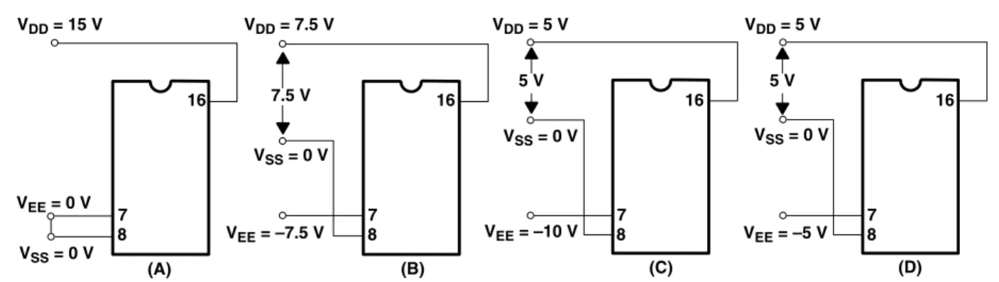
NOTE: The A, B, C, and INH input logic levels are L = VSS and H = VDD. The analog signal (through the TG) may swing from VEE to VDD.
7 8 (B) (C) (D) (A) 16 16 16 16 7 8 7 8 7 8 5 V 5 V VSS = 0 V VSS = 0 V VSS = 0 V VSS = 0 V VEE = –5 V VEE = –10 V VEE = –7.5 V VEE = 0 V VDD = 15 V VDD = 7.5 V VDD = 5 V VDD = 5 V 7.5 V
Figure 9. Typical Bias-Voltage Test Circuits
Figure 10. Channel Turned ON Waveforms
(R
L= 1 k
Ω
)
tf = 20 ns 10% 10% 90% 50% 10% 50% 90% 10% 50% 90% tr = 20 ns Turn-Off Time Turn-On TimeFigure 11. Channel Turned OFF Waveforms
(R
L= 1 k
Ω
)
tf = 20 ns 10% 90% 50% 10% 50% 90% 10% 90% tr = 20 nsTurn-Off Time Turn-On Time
PARAMETER MEASUREMENT INFORMATION
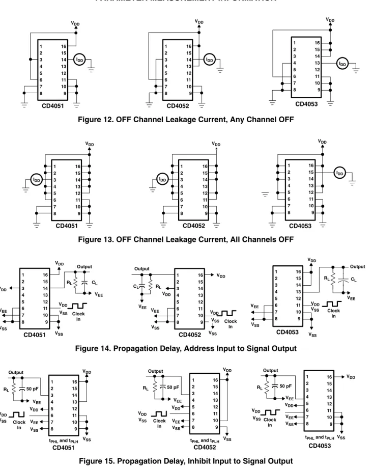
1 2 3 4 5 6 7 8 16 15 14 13 12 11 10 9 CD4051 VDD IDD CD4052 1 2 3 4 5 6 7 8 16 15 14 13 12 11 10 9 CD4052 VDD IDD 1 2 3 4 5 6 7 8 16 15 14 13 12 11 10 9 CD4053 VDD IDDFigure 12. OFF Channel Leakage Current, Any Channel OFF
1 2 3 4 5 6 7 8 16 15 14 13 12 11 10 9 CD4051 VDD IDD 1 2 3 4 5 6 7 8 16 15 14 13 12 11 10 9 CD4052 VDD IDD 1 2 3 4 5 6 7 8 16 15 14 13 12 11 10 9 CD4053 VDD IDD
Figure 13. OFF Channel Leakage Current, All Channels OFF
VSS RL CD4051 Clock In Output 1 2 3 4 5 6 7 8 16 15 14 13 12 11 10 9 VDD VDD VEE VSS VDD VSS VEE CL VDD CL CD4052 Clock In Output 1 2 3 4 5 6 7 8 16 15 14 13 12 11 10 9 VDD VSS VEE VDD VSS VSS VEE RL VDD VDD VEE VEE VSS VSS VSS CD4053 Clock In RL CL Output 1 2 3 4 5 6 7 8 16 15 14 13 12 11 10 9
Figure 14. Propagation Delay, Address Input to Signal Output
Output 1 2 16 15 50 pF VDD RL 1 2 3 16 15 14 Output 50 pF RL VDD 1 2 3 16 15 14 VDD Output RL 50 pF
PARAMETER MEASUREMENT INFORMATION
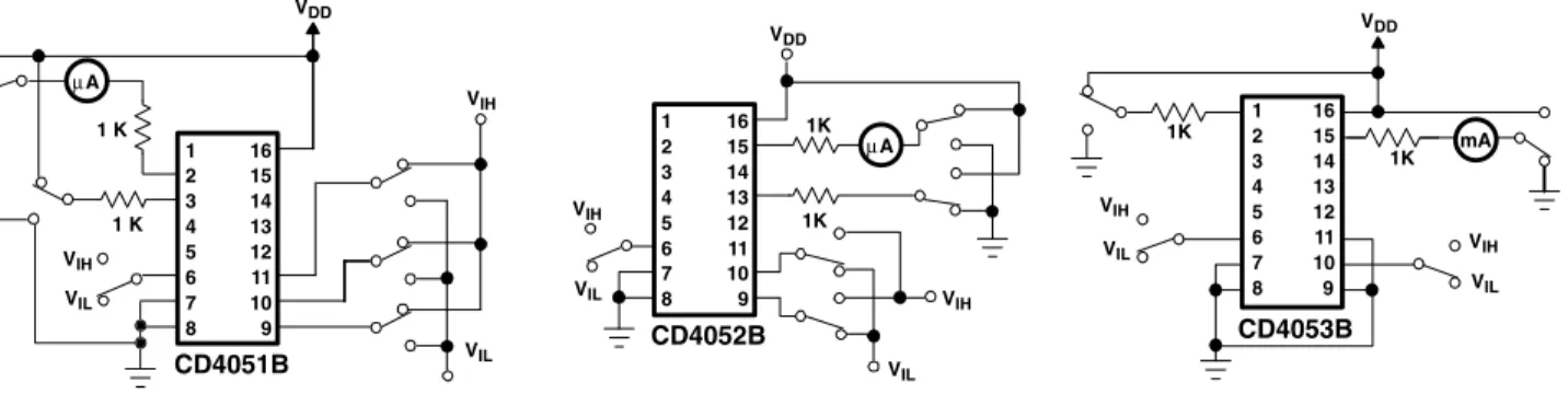
VIL CD4051B µA 1 2 3 4 5 6 7 8 9 10 11 12 13 14 15 16 VIH VIL VIH VDD 1 K 1 KMeasure <2 mA on All OFF Channels (e.g., Channel 6)
VIL VIH 1K 1K µA CD4052B 1 2 3 4 5 6 7 8 9 10 11 12 13 14 15 16
Measure <2 mA on All OFF Channels (e.g., Channel 2x) VDD VIH VIL VIL VIL VIH VIH 1K 1K VDD CD4053B 1 2 3 4 5 6 7 8 9 10 11 12 13 14 15 16
Measure <2 mA on All OFF Channels (e.g., Channel by) mA
Figure 16. Input-Voltage Test Circuit (Noise Immunity)
CD4051 CD4053 Ι 1 2 3 4 5 6 7 8 9 10 11 12 13 14 15 16 CD4052 Ι 1 2 3 4 5 6 7 8 9 10 11 12 13 14 15 16 VDD VDD
Figure 17. Quiescent Device Current
X Y TG On Keithley 610 Digital Multimeter H.P. Moseley 7030A X−Y Plotter 1-kW Range VDD VSS 10 kW
PARAMETER MEASUREMENT INFORMATION
NOTE: Measure inputs sequentially to both VDD and VSS.
Connect all unused inputs to either VDD or VSS. Ι CD4053 CD4051 1 2 3 4 5 6 7 8 9 10 11 12 13 14 15 16 VDD VSS VDD VSS
NOTE: Measure inputs sequentially to both VDD and VSS.
Connect all unused inputs to either VDD or VSS. Ι CD4053 CD4051 1 2 3 4 5 6 7 8 9 10 11 12 13 14 15 16 VDD VSS VDD VSS
Figure 19. Input Current
Figure 20. Feedthrough
RF VM OFF Channel 6 7 8 1K 5 VP−P VDDFigure 21. Crosstalk Between Any Two Channels
RL Common ON Channel RL RF VM ON Channel RL OFF Channel RL RF VM OFF Channel 5 VP−P 5 VP−P RF VM ON or OFF Channel In Y RL RL ON or OFF Channel In X
Figure 22. Crosstalk Between Duals or Triplets (CD4052B, CD4053B)
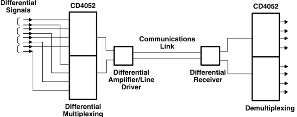
CD4052 CD4052
Communications Link Differential
APPLICATION INFORMATION
In applications where separate power sources drive V
DDand the signal inputs, the V
DDcurrent capability should
exceed V
DD/R
L(R
L= effective external load). This provision avoids permanent current flow or clamp action on the
V
DDsupply when power is applied or removed from the CD4051B, CD4052B, or CD4053B.
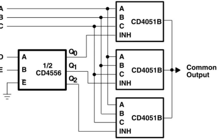
A B E 1/2 CD4556 A B C CD4051B INH A B C CD4051B INH A B C CD4051B INH A B C D E Q0 Q1 Q2 Common Output
www.ti.com 28-Feb-2014
PACKAGING INFORMATION
Orderable Device Status
(1)
Package Type Package Drawing Pins Package Qty Eco Plan (2) Lead/Ball Finish (6) MSL Peak Temp (3)
Op Temp (°C) Device Marking
(4/5)
Samples
CD4051BQPWRG4Q1 ACTIVE TSSOP PW 16 2000 Green (RoHS
& no Sb/Br)
CU NIPDAU Level-1-260C-UNLIM -40 to 125 CM051BQ
CD4051BQPWRQ1 ACTIVE TSSOP PW 16 2000 Green (RoHS
& no Sb/Br)
CU NIPDAU Level-1-260C-UNLIM -40 to 125 CM051BQ
CD4053BQM96G4Q1 ACTIVE SOIC D 16 2500 Green (RoHS
& no Sb/Br)
CU NIPDAU Level-1-260C-UNLIM -40 to 125 CD4053Q
CD4053BQM96Q1 ACTIVE SOIC D 16 2500 Green (RoHS
& no Sb/Br)
CU NIPDAU Level-1-260C-UNLIM -40 to 125 CD4053Q
(1)
The marketing status values are defined as follows:
ACTIVE: Product device recommended for new designs.
LIFEBUY: TI has announced that the device will be discontinued, and a lifetime-buy period is in effect.
NRND: Not recommended for new designs. Device is in production to support existing customers, but TI does not recommend using this part in a new design. PREVIEW: Device has been announced but is not in production. Samples may or may not be available.
OBSOLETE: TI has discontinued the production of the device.
(2)
Eco Plan - The planned eco-friendly classification: Pb-Free (RoHS), Pb-Free (RoHS Exempt), or Green (RoHS & no Sb/Br) - please check http://www.ti.com/productcontent for the latest availability information and additional product content details.
TBD: The Pb-Free/Green conversion plan has not been defined.
Pb-Free (RoHS): TI's terms "Lead-Free" or "Pb-Free" mean semiconductor products that are compatible with the current RoHS requirements for all 6 substances, including the requirement that
lead not exceed 0.1% by weight in homogeneous materials. Where designed to be soldered at high temperatures, TI Pb-Free products are suitable for use in specified lead-free processes.
Pb-Free (RoHS Exempt): This component has a RoHS exemption for either 1) lead-based flip-chip solder bumps used between the die and package, or 2) lead-based die adhesive used between
the die and leadframe. The component is otherwise considered Pb-Free (RoHS compatible) as defined above.
www.ti.com 28-Feb-2014
Important Information and Disclaimer:The information provided on this page represents TI's knowledge and belief as of the date that it is provided. TI bases its knowledge and belief on information
provided by third parties, and makes no representation or warranty as to the accuracy of such information. Efforts are underway to better integrate information from third parties. TI has taken and continues to take reasonable steps to provide representative and accurate information but may not have conducted destructive testing or chemical analysis on incoming materials and chemicals. TI and TI suppliers consider certain information to be proprietary, and thus CAS numbers and other limited information may not be available for release.
In no event shall TI's liability arising out of such information exceed the total purchase price of the TI part(s) at issue in this document sold by TI to Customer on an annual basis.
OTHER QUALIFIED VERSIONS OF CD4051B-Q1, CD4053B-Q1 :
•
Catalog: CD4051B, CD4053B•
Military: CD4051B-MIL, CD4053B-MILNOTE: Qualified Version Definitions:
•
Catalog - TI's standard catalog productTAPE AND REEL INFORMATION
*All dimensions are nominal
Device Package Type Package Drawing Pins SPQ Reel Diameter (mm) Reel Width W1 (mm) A0 (mm) B0 (mm) K0 (mm) P1 (mm) W (mm) Pin1 Quadrant CD4051BQPWRG4Q1 TSSOP PW 16 2000 330.0 12.4 6.9 5.6 1.6 8.0 12.0 Q1 CD4051BQPWRQ1 TSSOP PW 16 2000 330.0 12.4 6.9 5.6 1.6 8.0 12.0 Q1
*All dimensions are nominal
Device Package Type Package Drawing Pins SPQ Length (mm) Width (mm) Height (mm)
CD4051BQPWRG4Q1 TSSOP PW 16 2000 367.0 367.0 35.0
complete. All semiconductor products (also referred to herein as “components”) are sold subject to TI’s terms and conditions of sale supplied at the time of order acknowledgment.
TI warrants performance of its components to the specifications applicable at the time of sale, in accordance with the warranty in TI’s terms and conditions of sale of semiconductor products. Testing and other quality control techniques are used to the extent TI deems necessary to support this warranty. Except where mandated by applicable law, testing of all parameters of each component is not necessarily performed.
TI assumes no liability for applications assistance or the design of Buyers’ products. Buyers are responsible for their products and applications using TI components. To minimize the risks associated with Buyers’ products and applications, Buyers should provide adequate design and operating safeguards.
TI does not warrant or represent that any license, either express or implied, is granted under any patent right, copyright, mask work right, or other intellectual property right relating to any combination, machine, or process in which TI components or services are used. Information published by TI regarding third-party products or services does not constitute a license to use such products or services or a warranty or endorsement thereof. Use of such information may require a license from a third party under the patents or other intellectual property of the third party, or a license from TI under the patents or other intellectual property of TI.
Reproduction of significant portions of TI information in TI data books or data sheets is permissible only if reproduction is without alteration and is accompanied by all associated warranties, conditions, limitations, and notices. TI is not responsible or liable for such altered documentation. Information of third parties may be subject to additional restrictions.
Resale of TI components or services with statements different from or beyond the parameters stated by TI for that component or service voids all express and any implied warranties for the associated TI component or service and is an unfair and deceptive business practice. TI is not responsible or liable for any such statements.
Buyer acknowledges and agrees that it is solely responsible for compliance with all legal, regulatory and safety-related requirements concerning its products, and any use of TI components in its applications, notwithstanding any applications-related information or support that may be provided by TI. Buyer represents and agrees that it has all the necessary expertise to create and implement safeguards which anticipate dangerous consequences of failures, monitor failures and their consequences, lessen the likelihood of failures that might cause harm and take appropriate remedial actions. Buyer will fully indemnify TI and its representatives against any damages arising out of the use of any TI components in safety-critical applications.
In some cases, TI components may be promoted specifically to facilitate safety-related applications. With such components, TI’s goal is to help enable customers to design and create their own end-product solutions that meet applicable functional safety standards and requirements. Nonetheless, such components are subject to these terms.
No TI components are authorized for use in FDA Class III (or similar life-critical medical equipment) unless authorized officers of the parties have executed a special agreement specifically governing such use.
Only those TI components which TI has specifically designated as military grade or “enhanced plastic” are designed and intended for use in military/aerospace applications or environments. Buyer acknowledges and agrees that any military or aerospace use of TI components which havenotbeen so designated is solely at the Buyer's risk, and that Buyer is solely responsible for compliance with all legal and regulatory requirements in connection with such use.
TI has specifically designated certain components as meeting ISO/TS16949 requirements, mainly for automotive use. In any case of use of non-designated products, TI will not be responsible for any failure to meet ISO/TS16949.
Products Applications
Audio www.ti.com/audio Automotive and Transportation www.ti.com/automotive
Amplifiers amplifier.ti.com Communications and Telecom www.ti.com/communications
Data Converters dataconverter.ti.com Computers and Peripherals www.ti.com/computers
DLP® Products www.dlp.com Consumer Electronics www.ti.com/consumer-apps
DSP dsp.ti.com Energy and Lighting www.ti.com/energy
Clocks and Timers www.ti.com/clocks Industrial www.ti.com/industrial