CDM Protection, Testing and Factory Monitoring is
Easier Than You Think
Timothy J. Maloney
Intel Corporation Santa Clara, CA 95052 USA [email protected]Abstract– Charged Device Model (CDM) ESD events happen to semiconductor components during mechanical handling, mostly in assembly and test facilities. CDM-related product design and factory static control aim to prevent lasting damage to the component due to CDM events. Recently we have improved understanding of the CDM event, improved modeling of what CDM testers do, and improved measurement and simulation of factory CDM events. New tools for these activities are described. We now know the CDM experience of a typical component through its lifetime much better, and can express it in terms of CDM tester stress voltages. This allows the goal of low CDM-related manufacturing defects to be accessible, as on-chip designs can be made consistent with product performance as well as with CDM test goals, and the designs checked with appropriate CDM testing. Design principles for on-chip CDM protection in silicon CMOS have long been known, but need constant review and revision as semiconductor technology scales and product goals change. These principles are reviewed in light of our recently improved understanding of handling stress as it relates to CDM tester stress.
Keywords – CDM, ESD, factory EMI, TLP, VF-TLP, metal heating, oxide failure, CMOS reliability.
1. INTRODUCTION
The Charged Device Model (CDM) has long been associated with mechanical handling of integrated circuits (ICs) and is cited as a reason for failure of those ICs [1,2]. The early awareness of CDM in the 1970s evolved into development of the first good CDM testers in the 1980s [3,4], continuing into the 1990s. At the same time, design principles for avoiding CDM-related oxide and metal failures in CMOS ICs were developed [5,6].
While CDM awareness has been with us for over three decades, and CDM-related component testing available nearly as long, only recently has improved understanding of the factory discharges been related back to the kind of stresses applied by the CDM tester [7,8]. With such an understanding, we can devise a statistical model of CDM destruction [7] while aiming
for conditions that result in low DPM (defects per million) fallout due to CDM. These advances have allowed us to target CDM performance levels and factory static control and monitoring programs in order to achieve low fallout, and have provided the required tools. This paper will emphasize those recent, critical advances along with reviewing the basics of the CDM phenomenon, CDM testing, and related design principles for ICs.
2. CDM EVENTS AND TESTERS
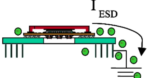
Components become charged during handling because of triboelectricity, or because of being moved into the region of an electric field. Triboelectric charging results from frictional contact by dissimilar materials, while E-field induction takes place near a surface (e.g., nonconductive plastic) that is already charged. CDM ESD stress results when a component under such influence connects to an equipotential surface (e.g., a pin touching grounded metal in a socket). Figure 1 shows a simplified view of a CDM event, with charge flowing on or off the component so that the potentials are equalized. For either the triboelectric or the E-field charging, the effective component area figures heavily in the total amount of CDM charge. For triboelectricity, charge is expected to be proportional to the interfacial contact area with the other surface, while for E-fields, Gauss’ Law
-I
ESD
-I
ESD
-I
ESD
-I
ESD
-I
ESD
Fig. 1. Simple view of charge flow between component and ground in CDM.
(normal E-field proportional to surface charge per unit area) indicates that charge goes as component area.
2.1 The Nonsocketed Charged Device Model (ns-CDM) Tester
as closely as possible. The original CDM machines were set up so that the CDM stress depends on the semiconductor package being used, the charge scales with package area, and so on. The Bell Laboratories CDM machine design [3,4] was the basis of test standards later adopted by the ESD Association and Jedec [9,10] for CDM testing; Figure 2 is from the Jedec spec and shows a field-induced CDM test system, so called because it literally uses a field plate to provoke charge flow on and off the component. This method is almost exactly equivalent to the direct charging CDM method, whereby a single pin (usually a substrate pin) charges the device with respect to a ground plane located under the dielectric, and the CDM zap is applied as usual. The ESDA CDM spec [9] allows for both direct charging and field-induced testing, and several commercial versions of the Fig. 2 test machine allow for both kinds of CDM testing.
Fig. 2. Non-socketed CDM machine, from [10].
2.2 Circuit Models for the ns-CDM Tester
The ns-CDM tester, shown in Fig. 2 and used in field-induced mode, can be circuit modeled as in Fig. 3 and the immediate charge packet Qimm calculated.
The importance of Qimm to CDM has been discussed
recently [7,8]. In Fig. 3, Cfrg is the capacitance from the top ground plane to the field plate, plus parastics. Cf is the capacitance of the component to the field plate, and Cg is the capacitance of the top ground plane to the component, both of which scale with component area. The ratio is Cg/Cf = tf/(εrtg), where
tf is the dielectric thickness (fractions of a mm plus
package dielectric), εr is the relative dielectric constant
of the dielectric (usually 3 to 4), and tg is the space
from the top ground plate to the package metal, roughly the pogo pin length of 5-7mm. Thus Cg/Cf is a small number. The field plate is charged to Vf through 300 MΩ. When the pogo pin touches the pin under test, the switch is closed and (neglecting overshoot effects) the resulting charge packet flowing immediately [7] is
(1) Usually, because of the thin dielectric, Cf is large and
Q2 is much more than Q1. This circuit model agrees
very closely with the charge packet as measured by integrating waveforms observed through the 50-ohm cable attached to the 1-ohm disk resistor [9,10].
Fig. 3. Circuit model for field-induced ns-CDM machine with component or test fixture in place. Switch closure happens when the pogo pin hits the component pin or test capacitor.
Direct charging was shown in [7] to be almost the same circuit model as Fig. 3 but not exactly. The charge packet Qimm for direct charging is nearly the
same as the field-induced model, but there is no factor of Cf/(Cg+Cf) in the expression, so direct charging
results in a factor of 1+Cg/Cf more charge, or 1+tf/(εrtg), not usually much of an increase. The
essentials of the above circuit model for field-induced charge were also in the 1989 paper on the ns-CDM machine [3]. The total amount of charge on the device at long times is Vf*Cf, considerably more than the Qimm charge. As discussed in [3], the residual
charge flows over a period of milliseconds and will not usually cause failure, but should also not be overlooked.
Note that the plate capacitance Cfrg includes more of Cf into Qimm as the package area gets smaller,
because as Cf becomes comparable to Cfrg (at least 4.3 pF), it is less reduced by Cfrg in the charge quantity Q2. So smaller-area packages suffer more
charge per unit area (which is proportional to E-field) when tested at a given voltage.
The peak CDM current Imax and its growth with package size [11] is related to these capacitance considerations. As most CDM events produce little ringing, the arc resistance (the R component) must be high enough to give near-critical damping. In addition, the equivalent capacitance, as above, helps explain the sublinear growth in Imax with package size, as observed in [11], as Cf is reduced by a relatively constant Cfrg. Further work on this subject is expected from the semiconductor industry.
3. CORRELATION OF FACTORY AND TESTER CDM EVENTS
From the early days of large-scale semiconductor manufacturing, factory static control engineers and .
1 Q
Q Cf
Cf
Vf ⎥= +
⎦ + + ⎥ ⎦ ⎢
⎣ + =
Vf
Cg 300 MΩ
Cf Cfrg
1 ohm disk resistor here dielectric to field plate
top gnd plane
*
2
Cfrg Cfrg Cf Cg Cg
Cf Qimm
⎤ ⎢
device design engineers have had to agree on sensible levels of static control as well as sensible levels of CDM protection on-chip. The most expedient combination of activities has been for each group to do whatever is “easy”, “cheap” and “obvious” in order to keep CDM-related fallout low. Rarely has it been necessary for both groups (and for many products, these are people at different companies) to cooperate intensively or even to adopt a common language in order to solve a problem. When there is a problem, usually one group or the other (which we will call design or factory) recognizes that they fell short of their usual standards, and should fix the problem. So in most cases, factory does not put excessive pressure on design, and vice versa. But we have now reached the need to know the relation between actual stress events in the factory and the ns-CDM tester events on the design side. The term “volts” on the factory side may have long been inspired by field meters, while “volts” on the design and test side is commonly a ns-CDM test voltage. The time has arrived to know the strength of actual CDM factory events and how to duplicate them with CDM testers [7,8].
3.1 Factory Static and Radiation Detectors
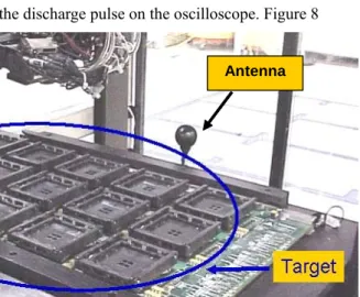
A trained user in the factory can use a broadband near-field antenna and a high speed oscilloscope for a low-cost, reliable means of detecting ESD and confirming ESD fixes [7]. The concept is essentially to detect the electromagnetic (EM) radiation emitted by an ESD event, a distinguishable EM signature. Figure 4 shows an E-field ball antenna (often used to detect EM interference or EMI) mounted near a component loader being monitored for ESD.
When an ESD event happens, the oscilloscope triggers and displays a waveform such as in Fig. 5. The dampened sinusoid, which has fast rise time, ringing in the hundreds of MHz, and decay over perhaps 50-75 nanoseconds, becomes familiar to the operator as the ESD signature. The antenna signal is a system response (equipment ground, antenna, cable, measurement instrument, etc.) to what is essentially a CDM impulse, lasting very few nanoseconds as is
well known [9-10]. The bandwidth of this impulse response usually tapers off well below the highest frequencies in the impulse, and the network is such that ringing persists for a long time (due to high Q), as seen in Fig. 5. The peak-to-peak voltage in this waveform, called Vp-p, appears to be the best indicator of the size of the impulse that produced it.
In a recent study [8], we introduced an instrument, connected to a voltage supply, which simulates the action of a charged component touching grounded factory equipment [12]. The schematic is in Fig. 6, and a top view of the PC board (32 mm dia) at the heart of the instrument is in Fig. 7. Essentially, a charged plate discharges when a peg mounted on the plate touches ground and passes the charge through a
z-matched transformer. The latter allows readout of the discharge pulse on the oscilloscope. Figure 8
Antenna
Fig. 4. Ball antenna set up near a component loader for burn-in boards.
Fig. 5. Typical waveform detected by ball antenna near component loader, showing ringing for 50-75 nanoseconds.
measured, using the charge instrument, for a given setup of factory equipment, the measured “real” CDM EMI events using the antenna take on new meaning. The Vp-p of those events now can indicate a CDM charge packet, suitable for relating to the ns-CDM machine’s Qimm as discussed above.
Fig. 6. Schematic diagram of discharge instrument, plus EMI antenna.
Fig. 7. Top view of board.
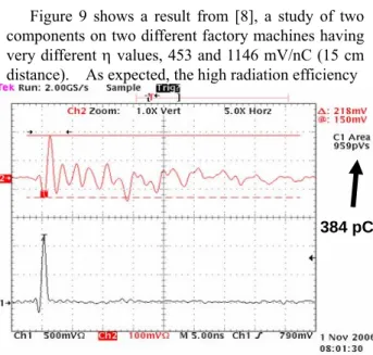
Figure 9 shows a result from [8], a study of two components on two different factory machines having very different η values, 453 and 1146 mV/nC (15 cm distance). As expected, the high radiation efficiency
Fig. 8. Scope traces; Ch. 1 discharge from grounded board at 100V, Ch. 2 from antenna 30 cm away. Result was 568mV/nC radiation efficiency, comparing Vp-p to charge packet.
equipment (1146 mV/nC) had many more metal surfaces. Once the equivalent capacitance Ceq and Ceq*V=Qimm was calculated for the two package sizes,
large and small, we could begin to estimate the equivalent CDM test voltage for each of the components given an imagined Vp-p of 400 mV from the antenna during real handling. Those equivalent voltages are in Fig. 9, with lower values considered “good” in light of our usual goal to pass a certain CDM voltage (e.g., 500V) for all components. For example, on the lower right if Fig. 9 we learn that a 400 mV Vp-p on the high η equipment for the large component means that component has been stressed at just 88.8V. But note how the same 400 mV measured for a small component on the low η system is equivalent to a worrisome 429V CDM. This result shows the utility of characterizing and monitoring the factory equipment in this way.
+V
1 M resistors
Ground plane charged
plate
EMI antenna
1:1 transformer, 50 ohm SMA and coax to scope
discharge line and peg
50 ohms
88.8 169
2 High η
225 429
1 Low η
2 large 1
small
88.8 169
2 High η
225 429
1 Low η
2 large 1
small
Component
Machine
transformer
Fig. 9. Factory results (CDM voltage stress levels at a fixed antenna Vp-p) for small and large components, as respectively measured on low and high radiation efficiency handler machines.
Hi-V line
3.2 Stochastic Model
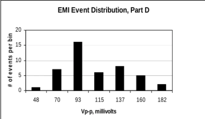
Now consider some factory data from “real” CDM events in Fig. 10, from [7]. How do we quantify the risk once we have the factory stress and also know the CDM test results for the component? To examine that, we developed a stochastic model to predict component fallout. Details of the model are in [7], but here is a brief summary. For a given component with m pins, the probability of destruction ∆ can be found by knowing F(q), the probability that a factory event’s charge packet is between the threshold of interest q0 and q (Fig. 10 helps to know this); φ1(k),
the probability that pin k will be hit; and φ2(q,k),
essentially the component test data or probability that pin k will be killed by charge q. Integrating over all charge packets and summing over all pins, this relationship is
384 pC
.
)
,
(
)
(
0
1
2
1
⎥
=
∆
⎦
⎤
⎢
⎣
⎡
∫
∞∑
=k
q
k
dq
dq
dF
q
m
k
φ
φ
(2)Conventional statistical methods tell us that if we have i sub-processes and an event rate λi, time Ti and
associated ∆i for each, then the expected component
(3)
With this model, the factory antenna data, radiation efficiency η, and CDM test data can all be merged to assess ESD risk to components in a highly rigorous way.
The data in Fig. 10 came from antenna readings on a pretty bad day for the equipment, before performing maintenance, changing belts, etc. Even so, all readings were below the 250 mV or so that is considered “bad”. Radiation efficiency η was at least a few hundred mV/nC. The large size of the component means that level of charge (~1nC) is reached at fairly low voltage in the ns-CDM machine, so there would have to be a notable CDM weakness to cause a problem. Thus a component is expected to survive this handler easily.
Fig. 10. Bin count (22.5 mV bins ending at each plot point) of EMI events for a 604-pin PGA component in a loader, where Vp-p is believed proportional to CDM charge packet.
3.3 Other CDM-related Test Methods
The focus thus far in this review has been on the ns-CDM tester [3-4,9-10]. While it is the most widely used and most standardized piece of equipment, there are other alternatives for simulating the Charged Device Model. One is the socketed CDM machine, sometimes known as the Socketed Device Model or SDM [13]. But there is only one vendor of the SDM tester, and present and future support for SDM appears to be limited. Even so, the convenience of socketing the part for a relay-based CDM-like test has helped to qualify many products at many companies. While the ns-CDM machine reproduces “real” CDM waveforms very well, its use in high-volume product qualification testing requires attention to such issues as probe wearout, probe cleaning, arc stability and reproducibility, humidity and atmosphere control—all issues related to the discharge of the arc in a controlled atmosphere. Improvements are being considered by various industry committees and manufacturers [14].
Another body of work on CDM-like tests has applied fast-pulse ESD characterization methods to the CDM problem, an approach called very-fast
transmission line pulsing or VF-TLP [15-17]. The work has been extended to capacitively coupled TLP or CC-TLP [16-17], which sets up a parallel plate capacitive ground return for the fast pulse and shows promise for applying CDM-like pulses at the wafer level. Failure analysis and waveform comparison has been used to demonstrate the utility and relevance of VF-TLP and CC-TLP to CDM. In somewhat related work, the present author has shown how to produce very strong VF-TLP pulses using coupled lines [18-19].
4. CDM PROTECTION IN SILICON CMOS TECHNOLOGY
A typical year’s Proceedings of this conference, or of the EOS/ESD Symposium, will yield extensive references to previous technical papers on chip protection, including CDM ESD. The CDM design journey began in the 1980s when we recognized that avoiding the conditions for oxide failure and metal failure [5-6] was paramount. Many design principles for CDM overlap with HBM, but some aspects are unique to CDM. A recent Ph.D. thesis study of CDM [20] reviewed and studied many of these CDM failure mechanisms, along with covering circuit modeling, testing methods and other device physics aspects.
Every CDM failure is subject to what could be called charge flow analysis. For CDM, remember that “charge is stored where the field lines end” (Gauss’ Law), so visualize the packaged device at a voltage with respect to an external ground plane. The E field
lines end mostly on the substrate, die paddle, etc., while much other charge may be only one diode drop away from Vss. Vcc is the only other node with charge storage considerable enough to cause CDM failure somewhere. Virtually all CDM failures in manufacturing result from all the charge on Vcc or Vss becoming concentrated at one small location. Thus in CDM failure analysis, concentrate first on how a LARGE amount of package charge could have found its way to that point. This principle leads one to find vulnerable oxide edges and metal choke points, as described in [5-6]. Most failure analysis for CDM can be put into these terms; it can be, as we are trying to show, easier than you think.
As integrated circuit technology advances, it provides us with new challenges, but also with new opportunities and new relief from old constraints. For example, as we face ever-shrinking line widths, oxide thicknesses, and supply and signal voltages, our ICs become harder to protect against essentially unscaled ESD events (as the human being and IC package size are not scaling much!), but at the same time those shrinking line widths have allowed a huge increase in MOSFET current per unit area of the silicon. This means sinking amps of current through ordinary MOSFET action (now used as the timed power supply
∑
∆
=
iT
DPM
10
λ
.
EMI Event Distribution, Part D
0 5 10 15 20
48 70 93 115 137 160 182
Vp-p, millivolts
# o
f e
ven
ts
p
e
r b
in
i i mfr
6
clamp) can be done now, while in the 1970s and 1980s it was absurd because of the huge area required.
The transition of CMOS IC metal from aluminum to copper was largely motivated by issues like electromigration and chip heating, but it also offered some relief for ESD protection. Copper, of course, has a melting point several hundred degrees higher than aluminum, and a higher specific heat on account of its higher atomic number, along with even lower resistivity. Studies resembling our early work on aluminum [6,21] were done at Intel on copper but remained unpublished. One recent example of a study of ESD and TLP on copper was published by TSMC [22].
Finally, speed of response of protection circuits to CDM events has always important, as inattention to that aspect has been responsible for some CDM failures [5]. In general, the response of well-designed diodes, power clamps and FETs (where often the FETs are in a parallel path with diodes) has been fast enough for adequate CDM protection. But some times a few pins have a design requirement like voltage tolerance that makes CDM hard to meet. Technology scaling can help in some of these cases—consider the case of the scaled SCR whose trigger time was reduced to the subnanosecond level [23]. This trigger time has been a problem for SCRs with respect to CDM (not HBM), but dimensional scaling should offer faster trigger times.
5. CONCLUSIONS
CDM ESD monitoring, modeling and tester simulation have made rapid advances. It is now possible to detect CDM events happening in assembly and test facilities, and relate that data to CDM component data taken on testers like the non-socketed CDM machine, as specified by ESDA and Jedec. A useful tool for risk assessment is a stochastic model that incorporates knowledge of the factory stress and of the component CDM test results to estimate fallout in a rigorous fashion. These recent efforts have resulted in improved CDM test expectations, cost savings, and well-targeted factory activities. The understanding between device and test workers on one side, and factory static control workers on the other, has also vastly improved.
Design principles for on-chip CDM protection in silicon CMOS have long been known, but need constant review and revision as semiconductor materials, size scales, and product goals change. CDM failures are most commonly caused by a large portion of the package charge being concentrated into a small volume on its way out of the component during the CDM event. The chief design exercise identifies and avoids destructive charge flow paths, and devises safe paths for charge flow. The high speed and high peak current of the CDM pulse present some unique
challenges that need to be overcome at each technology node. Some technology trends, like increased MOSFET current density and higher speed protection circuits due to scaled dimensions, work in favor of CDM protection. At the same time, the trend toward lower voltage breakdown of junctions and oxides, and a lower capacitance budget for higher speeds, correspondingly raises the CDM protection challenge. In the end, CDM protection in chip design and static control under manufacturing, test, and use conditions must meet each other halfway. With proper understanding of component handling and CDM performance, continued high-volume, low-cost manufacturing of CMOS semiconductor components should be achievable.
REFERENCES
[1] T.S. Speakman, “A Model for the Failure of Bipolar Silicon Integrated Circuits Subjected to Electrostatic Discharge”, International Reliability Physics Symposium (IRPS), pp. 60-69, 1974.
[2] P. R. Bossard, R. G. Chemelli and B. A. Unger, "ESD Damage from Triboelectrically Charged Pins," EOS/ESD Symp. 1980.
[3] R. Renninger, M-C. Jon, D.L. Lin, T. Diep and T.L. Welsher, “A Field-Induced Charged-Device Model Simulator”, EOS/ESD Symp. pp. 59-71, 1989. [4] R. Renninger, “Methods of Charged-Device Model
Electrostatic Discharges”, EOS/ESD Symp. pp. 127-143, 1991.
[5] T.J. Maloney, "Designing MOS Inputs and Outputs to Avoid Oxide Failure in the Charged Device Model", EOS/ESD Symp, pp. 220-227, 1988.
[6] T.J. Maloney, "Integrated Circuit Metal in the Charged Device Model: Bootstrap Heating, Melt Damage and Scaling Laws", EOS/ESD Symp., pp. 129-134, 1992. Also J. Electrostatics 31, pp. 313-321, 1993.
[7] J.A. Montoya and T.J. Maloney, “Unifying Factory ESD Measurements and Component ESD Stress Testing”, EOS/ESD Symp. pp. 229-237, 2005.
[8] T.J. Maloney, "Instrument for Calibrating Antenna-based ESD Detectors", 1st Annual
International Electrostatic Discharge Workshop (IEW), pp. 274-288, May 2007.
[9] ANSI-ESDSTM5.3.1-1999, “Charged Device Model (CDM)-Component Level Test Method”, ESD Association, 1999. See www.esda.org.
[10] JEDEC JESD22-C101-C standard, “Field-Induced Charged-Device Model Test Method for Electrostatic-Discharge-Withstand Thresholds of Microelectronic Components”, Dec. 2004. See www.jedec.org.
[11] A. Jahanzeb, Y-Y. Lin, S, Marum, J. Schichl, and C. Duvvury, “Influence of Device Body Size on CDM Tester Peak Current and its Variability”, 1st Ann. IEW
[12] T.J. Maloney, "Method and Apparatus for Simulating Electrostatic Discharge Events in Manufacturing and Calibrating Monitoring Equipment", US Patent Application (Intel), filed December 23, 2005.
[13] ANSI-ESDSP5.3.2-2004, “Socketed Device Model (SDM)-Component Level Standard Practice”, ESD Association, 2004. See www.esda.org.
[14] These topics were treated in discussion groups at the 1st Annual IEW, Fallen Leaf Lake, CA, May 2007.
[15] H. Gieser and M. Haunschild, “Very-Fast Transmission Line Pulsing of Integrated Structures and the Charged Device Model”, EOS/ESD Symp., pp. 85-94, 1996. Also IEEE CPMT (C), 21, pp. 278-285, Oct. 1998.
[16] H. Wolf, H. Gieser, W. Stadler, W. Wilkening, “Capacitively Coupled Transmission Line Pulsing CC-TLP—A Traceable and Reproducible Stress Method in the CDM Domain”, EOS/ESD Symp. pp. 338-345, 2003.
[17] H. Wolf, H. Gieser, “Investigations With the Capacitive Coupled TLP on Package and Wafer-Level”, 1st Ann. IEW, pp. 358-368, May 2007.
[18] T.J. Maloney and S.S. Poon, "Using Coupled Transmission Lines to Generate Impedance-Matched Pulses Resembling Charged Device Model ESD", EOS/ESD Symp. pp. 308-315, 2004. Also IEEE T-EPM 29, no. 3, pp. 172-178, July 2006.
[19] T.J. Maloney and S.S. Poon, “Using Coupled Lines to Produce Highly Efficient Square Pulses for VF-TLP”, EOS/ESD Symp. pp. 311-317, 2006.
[20] M. Etherton, “Charged Device Model (CDM) ESD in ICs: Physics, Modeling, and Circuit Simulation”, Konstanz: Hartung-Gorre Verlag Series in Microelectronics, Vol. 170 (Reprint of Diss. ETH No. 16354), 2006.
[21] T. Maloney and N. Khurana, "Transmission Line Pulsing Techniques for Circuit Modeling of ESD Phenomena", EOS/ESD Symp. pp. 49-54, 1985. [22] J.H. Lee, J.R. Shih, K.F. Yu, Y.H. Wu, J.Y. Wu, J.L.
Yang, C.S. Hou and T.C. Ong, “High Current Characteristics of Copper Interconnect under Transmission-Line Pulse (TLP) Stress and ESD Zapping”, IRPS, pp. 607-608, 2004.
![Fig. 2. Non-socketed CDM machine, from [10].](https://thumb-us.123doks.com/thumbv2/123dok_us/8195555.2172645/2.892.463.786.189.370/fig-non-socketed-cdm-machine.webp)