Evaluating TLP Transients and HBM Waveforms
Timothy J. Maloney
Intel Corporation, 3601 Juliette Lane, Santa Clara, CA 95054 USA tel.: 408-765-9389, e-mail:[email protected]
This paper is co-copyrighted by Intel Corporation and the ESD Association
Abstract –Transmission Line Pulsing (TLP) is capable of determining a true impedance function in the
s-domain, including time-dependent transients, as Z=Z1(1+as+bs2+…), with nonzero s-coefficients. We show
how to determine the Z1 and a terms and how to find more terms if desired, for long and short TLP pulses,
drawing on network theory and approximation methods. We apply these to examples of inductive delay in devices. The same kind of methods are used to remove the effects of measurement tools themselves, including finite rise time of the TLP pulse and voltage droop of a current transformer. Then the true RC time constant of an HBM waveform is extracted as a network coefficient, through methods developed in this work.
I. Introduction
For about the last 25 years, semiconductor TLP
characterization of ESD behavior [1] has centered
on steady-state I-V, equivalent to finding,
point-by-point, an equivalent DUT impedance. While
works like [1] touched on finding capacitance or
inductance from i-t and v-t plots, the focus was
on steady-state response to the TLP step. But
structured methods are available for
characterizing DUT transients, first by finding
first-order frequency dependence and setting the
stage for higher-order characterization.
This work presents systematic TLP methods for
finding DUT impedance Z
1(1+
a
s), where Z
1is
the usual dc impedance, s the complex frequency
σ
+j
ω
, and
a
Z
1is the s-coefficient, describing a
one-pole response. Z
1and
a
Z
1can be calculated
through 0
thand 1
storder moments (integrals and
centroids) of the TLP waveforms, respectively,
although it will be shown how familiar
step-response TLP to steady state requires only
integration of the waveform in order to extract
the s-coefficient. Essentially the same
observations apply to the admittances Y
1and
a
Y
1, in shunt networks complementary to the
presumed series network with impedance
Z
1(1+
a
s). Higher order terms in the expansion of
Z
1or Y
1in s can then be found from the higher
order waveform moments.
The methods can also be extended to very fast
TLP (VF-TLP) cases where the waveforms are
too short to find a clear steady state. With proper
calibration pulses for comparison, much essential
modeling information can still be extracted.
Convolution techniques and theorems are used to
formulate the methods and prove the
relationships.
These methods are applied to some examples of
time dependent response. One is ferrite
inductance and resistance as extracted from step
pulse response, and the other is a model of
diode-triggered SCR overshoot response to a TLP
step. The very same concepts can be applied to
circuits with a shunt capacitance.
II. Step Response Solution
1. Waveform Analysis and Networks
Traditional Transmission Line Pulsing (TLP) could be described as examining a device’s step response out to a time where steady voltage Vd and current Id are
achieved, giving a steady-state Z1= Vd/Id. But this is
just the first term of what is presumed to be a (locally) linear, time-invariant network, and the true impedance function in the s-domain, describing the transients as well, would be Z=Z1(1+as+bs2+…), s=σ+jω, with
nonzero s-coefficients. An objective in this paper is to examine the a term, for basic inductive or
capacitive response, and to show how to find more terms if desired.
In the TDR-TLP method [2,3], although the others could be used too, we obtain device voltage and current from
)
(
)
(
)
(
t
V
t
V
t
V
=
++
− , 0)
(
)
(
)
(
Z
t
V
t
V
t
I
=
+−
−, (1)
while still knowing our outgoing pulse from V+. The
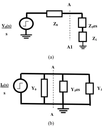
prototype circuits for this characterization are in Fig. 1, showing impedances Z, admittances Y, and step voltage and current sources that may not be ideal.
(a)
(b)
Figure 1: a) Thevenin equivalent step-driven TLP circuit with transient. b) Norton equivalent. Device is at plane A-A1.
The equations for networks (a) and (b) in Fig. 1 are similar and have complementary solutions, so we will focus on (a), best suited to an inductive transient. The device voltage Vd at plane A-A1 responding to a step
voltage is, in the complex frequency or s-domain,
s
s
V
as
Z
Z
Z
as
Z
Z
s
V
d(
)
0(
)
1 1 0
1 1
+
+
+
=
.
,
)
(
)
(
0 1
1 0
1
1
Z
Z
Z
X
s
s
V
as
X
as
X
div div
div
+
=
+
+
=
(2)Expanding the ratio to first order we have
s s V as X X
s
Vd div div
) ( ...] )
( [ )
( = 1+ 1− + 0 (3)
The coefficient of V0(s)/s in (3) is the transfer
function; call it X1(s). We differentiate to get the
impulse response, which is
)
)
(
(
)
(
dt
t
dV
s
sV
dd
=
L
).
(
...]
)
(
[
X
div+
X
div1
−
X
divas
+
V
0s
=
(4)We use L( ) to denote the Laplace transform of dVd(t)/dt. According to the convolution theorems in
[4] (p. 111), the time-domain areas of convolved functions, as in (4), multiply, and the time domain centroids add, so that
A
0 1
0 1 0
)
(
Z
Z
V
Z
V
X
t
V
d div+
=
=
∞
→
(5), andZ0
V0(s)
s
Z1as
Z1
0
1 V
X dt
dV
t
t
t
d=
+
,A1
where
.
)
(
)
(
0 0
∫
∫
∞ ∞
=
dt
t
f
dt
t
tf
t
f (6)
The leading term, Z1, computes as usual. Note that 〈t〉Vo is the centroid of the differentiated incoming
step.
In work pioneered by Elmore [5] and continued in more recent works [6,7], it is shown that a waveform
h(t) is transformed into the Laplace domain by
expanding the exponent in the transform as follows:
I0(s)
s
Y0 Y1as
A
Y1
∫
∞ −=
0dt
e
t
h
s
H
(
)
(
)
st∫
∞⋅⋅
⋅
+
−
+
−
=
0 3 3 2 26
2
1
st
s
t
s
t
dt
t
h
(
)[
]
∑
∞∫
= ∞−
=
0 01
k k k kdt
t
h
t
s
k
!
(
)
.
)
(
(7)
Equation (5), above, is about the first term, the waveform integral or 0th moment. The second term
(i.e., the first moment k=1 in the moment expansion)
determines the s-coefficient of H(s). Thus we can
find the DUT impedance, Z1(s)=Z1(1+as).
Integration by parts [8] states that if f(t) and g(t) are two continuously differentiable functions, then given an interval with endpoints a, b, one has
∫
∫
′
=
−
b′
a b a b a
dt
t
g
t
f
t
g
t
f
dt
t
g
t
f
(
)
(
)
[
(
)
(
)
]
(
)
(
)
. (8)
Our main case is a=0, b=t1 (integration to somewhere
in the flat part of Vd(t)), f(t)=t, g(t)=Vd(t), and
Vd(0)=0. Thus
∫
∫
1=
−
10 0
1
1
(
)
(
)
)
(
td t
d
d
dt
t
V
t
V
t
dt
dt
t
dV
t
. (9)
To get the centroid, we normalize as in Eq. (6) by dividing (9) by
0 1 0 1 0 1 0
)
(
)
(
1Z
Z
V
Z
V
X
t
V
dt
dt
t
dV
div d t d+
=
=
=
∫
. (10)
The same kind of thing is done to V0(s) to calculate its
centroid from V+(t), which flattens out at V0/2. More
about correcting for V0(s) is in Section IV.
The integration limit t1 in Equations (9-10) can stop
anywhere on the flat (derivative is zero) part of Vd(t)
because nothing is added to the centroid in that region. Now we have
,
)
(
∫
+
−
=
1 0 0 1 0 1 1 t d dtdV
V
t
dt
V
Z
Z
Z
t
t
d∫
+ − = 1 0 0 0 1 2 tV t V V t dt
t ( )
. (11)
This gives
∫
∫
−
+
=
1 + 11 0 0 1 0 1 0 0
)
(
)
(
2
t d tX
Z
V
V
t
dt
Z
Z
dt
t
V
V
t
. (12)
These integrals also cancel beyond a t1 when the
voltages V+ and Vd go flat. But from Eqs. (4) and
(7),
we know that
1 0
0
1
Z
Z
a
Z
t
X
=
−
+
; therefore thes-coefficient or effective inductance is
eff
L
a
Z
1=
⎥
⎦
⎤
⎢
⎣
⎡
−
+
+
=
∫
1∫
1 +0 0 0 0 1 0 1 0 1 0
1 t
2
td
V
t
dt
V
dt
t
V
V
Z
Z
Z
Z
Z
Z
Z
)
(
)
(
)
(
∫
−−
++
=
1 0 0 0 0 2 1 0 tdt
t
V
t
V
V
Z
Z
Z
)]
(
)
(
[
)
(
ρ
(13)
This theorem can also be put in terms of Laplace transforms: For a network function (impulse response) N(s) = a0+a1s+a2s2+…, the step response
gives a0/s+a1+a2s+…. Subtract the dc offset and the a0
term is gone; integrate this new waveform (i.e., apply 1/s) and the new dc offset gives the first moment a1.
Higher-order moments can be extracted by successive reduction of waveforms in this fashion.
For the above inductor in a series circuit with total resistance Z0+Z1, the impact on Z1 rise time (Elmore
Delay) is
1
0
Z
Z
L
t
D eff+
=
⎥
⎦
⎤
⎢
⎣
⎡
−
+
=
∫
1∫
1 +0 0 0 0 1 0 1 0
1 t
2
td
V
t
dt
V
dt
t
V
V
Z
Z
Z
Z
Z
)
(
)
(
∫
−−
++
=
1 0 0 0 0 1 0 tdt
t
V
t
V
V
Z
Z
Z
)]
(
)
(
[
)
(
ρ
. (14)
ρ0 is (Z1-Z0)/(Z0+Z1). Note that there is no difficulty
for Z1=Z0 or for Z1 approaching zero. For the case of
negligible rise time or overshoot on the input pulse, these equations simplify to
⎥
⎦
⎤
⎢
⎣
⎡
+
−
+
=
∫
0 1 1 1 0 0 0 0 2 0 1 1Z
Z
t
Z
V
dt
t
V
Z
V
Z
Z
L
eff(
)
t d(
)
(15)Now the coefficient of t1 is Vd(t1), the final voltage,
and it’s even clearer why the integration limit t1 is not
waveform. Thus the graphical view of Eq. 14, in Fig. 2, shows matched rising edges for the two waveforms whose areas will be subtracted. The inductance and time delay is then computed from the overshoot-only area as shown.
Figure 2: Time delay or inductance as derived from the difference of two areas, as in Eq. (14).
2. Ferrite Example
An example of this is found in the analysis of Figures 3 and 4, showing an overshooting TLP voltage pulse resulting from a step input to an 11-ohm resistor with a ferrite slipped over one of the resistor leads. This creates an inductance and, as we shall see, series and parallel resistances. Figure 3 shows the result at a short time scale (2.5 nsec/div), with overshoot due to the wire inductance, while Figure 4, at 1 µsec/div, shows overshoot due to the (considerably larger) ferrite inductance.
Figure 3: Voltage waveform of 11 ohm resistor plus ferrite on a resistor lead. Short time scale shows wire inductance (30 nH) and additional resistance values.
In Fig. 3, we find that 390 mV (after 100X attenuation) compares with 760 mV open circuit, giving a long-term Z1 impedance of 52.7 ohms. This
means that the ferrite adds 41.7 ohms to the circuit, plus its inductance. The overshoot peaks at 560 mV, short of the open circuit value, approximated by the
added inductance being in parallel with about 98 ohms. It is approximate because finite rise time has an effect, to be discussed later. Fig. 4 shows a long-term decay of voltage due to ferrite inductance. We integrate the overshoots to find inductances and complete the resulting network (Figure 5). The inductance of 30.2 nH, from the fast waveform, is
Figure 4: Voltage waveform of 11 ohm resistor plus ferrite on a resistor lead. Longer time scale shows ferrite inductance (25 µH) and confirms resistance values.
Figure 5: Circuit model of 11 ohm resistor plus ferrite, from waveform analysis at two time scales.
about right for the resistor wire itself. Over a period of 5.5 µsec, the sustaining voltage declines to a level appropriate to the remaining 11 ohm resistor, as expected. This gives 25.4 µH in parallel with the 42 ohms as the ferrite contribution, as in Fig. 5.
V
d(t
1)t
1-rise area
V
dt
Voltage integral
t
130 nH
98 ohms
42 ohms
25
µ
H
3. Diode Example
The forward-biased diode is of course the most common ESD protection device. The best protection diodes respond quickly to fast pulses but some overshoot of the final voltage has been seen if a fast enough step was applied. As VF-TLP has advanced, rise times have shortened and the overshoot of well-designed ESD protection diodes and associated circuits are being more clearly measured. Figure 6, from this same conference [9], is a good example of overshoot from a diode-triggered silicon controlled rectifier (DTSCR), incorporating both the diode and SCR delay.
Figure 6: VF-TLP measurement of the overshoot transient behavior of a DTSCR [9].
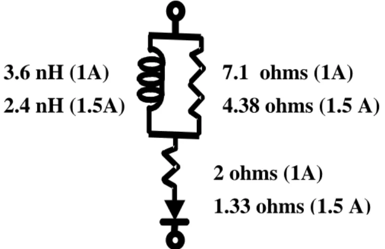
Figure 7: Circuit model for DTSCR as computed from waveforms in Fig. 6.
The overshoot shown in Fig. 6 is almost the same for the 1A and 1.5A cases (50 ohms, for 53V and 79V line charge), while the 8V peak indicates a noticeable parallel resistance in the equivalent circuit, exclusive of rise time effects. This means that the equivalent circuit will depend on pulse voltage and current, as shown in Figure 7. This is not surprising, given that the delay times and overshoots are semiconductor
phenomena, nonlinear and nonmagnetic. Even so, models such as in Fig. 7 are useful in ESD circuit simulation.
How much this circuit model, or even device behavior itself, depends on the measurement system is not known. As the TLP impedance Z0 affects the Elmore
Delay (Eqs. 14-15), the waveform could change for 1A or 1.5A final current if the load line Z0 is different.
This could be an interesting item for future study.
4. Other Conditions
For the common case of current overshoot and voltage gradually approaching a limit, one will apparently have negative inductances and time delays, which are still meaningful. But the model in Fig. 1b, entirely complementary, would give positive aY1, or Ceff, and
positive tD=Ceff/(Y0+Y1), and could be more agreeable
for data records. Figure 2 still applies if the device current is plotted instead of voltage, although integration of the voltage undershoot due to capacitance is an equally acceptable way to calculate it [10], as would be integrating the current undershoot to find inductance. Indeed, the Elmore Delay is most commonly represented as an R-C phenomenon, as in [10]. The present work’s treatment shows exactly the same moment-matching method in equivalent and complementary terms, and thus demonstrates the power of the technique for both inductive and capacitive transients. If one substitutes
V0ÆI0
Z0ÆY0
Z1ÆY1
3.6 nH (1A)
2.4 nH (1.5A)
7.1 ohms (1A)
4.38 ohms (1.5 A)
VdÆId
V+,-ÆI+,-
in Eq. 13 and uses the Norton network (Fig. 1b), one gets Ceff=Y1a and a method of finding Ceff.
2 ohms (1A)
1.33 ohms (1.5 A)
The ease of determining Leff or Ceff with the above
methods could allow a needle probe pair as in [11] to be modeled as a high-Z transmission line by finding Leff for a shorting load and Ceff for an open load.
Equation 13, and its equivalent for capacitance, describes the proper waveform area differences, and accounts for the finite rise time of the source. With Leff and Ceff, the transmission line transfer function
could be used for de-embedding various devices being probed, and would comprehend load-dependent effects. Thus if needle probes of high impedance
eff eff
line L C
Z = /
and electrical length l connect to a load ZL, the impedance looking into the needle
,
,
tan
tan
L line lineZ
Z
r
l
j
r
l
jr
Z
Zin
⎥
=
⎦
⎤
⎢
⎣
⎡
+
+
=
β
β
1
, c l C L l eff effω
ω
β
= =(16)
c the propagation velocity on the needle probe line.
In s-domain terms, tan(βl) could be replaced by tanh(ks), approximated by ks-(ks)3/3+... Eq. 16 thus
gives all we need to find ZL (and not just
low-impedance loads) given a first-order measurement of Zin=Z1(1+as). The latter is derived by measuring step
response and transients as described earlier.
III. Short Pulse Solution
TLP as step response is the most comfortable situation for analyzing the transients. Even if VF-TLP methods are used [3], if the steady-state is achieved in a short response time, the above analysis can be used. But sometimes transients will not finish and falling pulse edges will have to be comprehended along with the usual rising edges.
In such a case we make use of the fact that the pulses return to zero, and therefore have their own moment series without taking derivatives. The short incoming pulse is, in effect, an approximation of an impulse. The responding device voltage thus approximates an impulse response or transfer function. To quantify this, we return to Fig. 1 and replace the step voltage source with a V0(s)/s representing the near-rectangular
VF-TLP pulse. In the s-domain, the perfect rectangular “boxcar” function of length ∆t is
s
e
V
s
s
V
ts)
(
)
(
−
−∆=
01
0 , (17)
also expressible in sin x/x form. Let this correspond to V0(t). In any case, Eq. 3 applies, where now
s
s
V
as
X
X
X
s
V
d(
)
=
[
div+
div(
1
−
div)
+
...]
0(
)
(18)and following Eqs. 5-7, the 0th and first moments can be matched to determine the coefficients of X1(s), the
coefficient of V0(s)/s in (18):
∫
∫
∞ ∞
=
0 0
0
t
dt
V
X
dt
t
V
d(
)
div(
)
, (19)0
1 V
X
V
t
t
t
d
+
=
. (20)Short pulse waveform integrals as in (19) determine Z1, while Z1a now results from actual computation of
the centroids, with units of time, as in (20). In accordance with (7) and (20),
0 1 1 0 0 V V
X
Z
Z
t
t
a
Z
t
d−
=
+
−
=
, (21)and
[
]
0 1 0 1 1 0
Z
Z
Z
Z
t
t
L
a
Z
d V V eff)
(
+
−
=
=
. (22)Positive Leff results when the overshoot on Vd
produces a centroid value less than that of the incoming waveform V0.
IV. Waveform Corrections
1. Inverse Filtering and Deconvolution
TLP transients will sometimes be on the same time scale as the TLP rise time. For example, in Fig. 3 and Fig. 6, a detailed TLP calibration waveform into a 50 ohm load should help find a more nearly ideal step response for the device under test.
In earlier sections, the generalized s-domain TLP step is given as V0(s)/s. With V0(s), we can invert it,
multiply the original waveform (in the s-domain; call it W(s)), and transform to the time domain for the corrected waveform Wc(t). A frequency domain
representation of V0(s) is sufficint; consider this
simple example.
Starting with digital data of a calibration step into 50 ohms (call it Vcal(t)), we differentiate to get
).
(
)
(
)
(
)
(
s
V
s
s
sV
t
V
dt
t
dV
cal 0 00
⇔
=
=
(23)V0(t) looks like a short pulse; with methods described
earlier to find the centroid τr of this pulse, we can
transform V0(t) into V0(s) after approximating V0(t).
The centroid τr is the rise time of a 1-pole exponential
approach expression for the Vcal(t) waveform, and if a=1/τr, we have
)) exp( ( ) ( r cal t V t V
τ
− − = 0 1. ) ( ) ( ) ( s s V a s s V s Vcal 0 0 = + =
⇔ (24)
Thus to restore our “perfect”step function V0/s, we
multiply Vcal(s) by s+a, and similarly with W(s) to
find Wc(s) and eventually Wc(t). The convolution
theorem cited earlier [4] provides guidance.
Multiplying by s+a means to differentiate the step
response W(t) (s is the differential operator) and add to it an amount of W(t) proportional to a, the
give a Wc(t) that is much the same as W(t), with little
correction due to the derivative. Conversely, a step response dominated by TLP rise time will show more of a true step response, of the device only, consistent with noise limits of the measuring system.
Notice that our one-pole approximation of Vcal(t) was
a “simple example”, arbitrarily chosen. We could have chosen to take more moments to find a multi-pole fit for V0(s) and Vcal(s), resulting in a more
complicated inverse filter expression, and improving approximations of the waveform, ever-closer to the noise limit of the channel. Indeed, we could take the digital calibration data and do a computer-based fast Fourier transform (FFT) to find out as much as possible about V0(s). That would take
us to Wiener deconvolution [12,13], a
long-established signal processing method. This would make maximum use of the calibration data in order to remove its influence from the final measurement. To correct the above waveform W(s) with a Wiener filter G(s) so that G(s)W(s)=Wc(s), the Wiener
deconvolution theorem [12,13] states that
⎥
⎥
⎥
⎥
⎦
⎤
⎢
⎢
⎢
⎢
⎣
⎡
+
=
)
(
)
(
)
(
)
(
)
(
s
SNR
s
V
s
V
s
V
s
G
1
1
2 0
2 0
0
, (25)
where SNR(s) is the frequency-dependent signal-to-noise ratio. In the absence of signal-to-noise, for infinite SNR(s), this is exactly the 1/V0(s) inverse filter that
we used above. But it is clear that any (s+a) filter
needs to pay attention to noise, at least at low and high frequency, and roll off accordingly.
Many modern oscilloscopes have the digital signal processing (DSP) and math functions required for complete inversion of a measurement channel transfer function like V0(s). This allows measured waveforms
to be processed by a user-defined finite impulse response (FIR) filter [14]. The FFT math function alone (present in many digital oscilloscopes) should allow a first moment to be measured by taking a slope at low frequency. As these tools become more common, it is very likely that ESD waveform measurement and calibration will make use of them more often.
2. Practical Example, HBM Waveform
An interesting yet simple case of inverse filtering would be to examine the 0-ohm ~150 nS decay constant of the human body model (HBM) ESD tester according to ESDA and JEDEC standards [15,16]. The required current transformer is or resembles the Tektronix CT-1, which is specified with a minimum
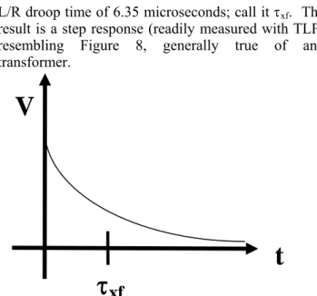
L/R droop time of 6.35 microseconds; call it τxf. The
result is a step response (readily measured with TLP) resembling Figure 8, generally true of any transformer.
V
t
Figure 8: Step response of a transformer; τxf is the 1/e decay time.
τ
xf
Impulse response would be the derivative of Fig. 8, meaning a spike at zero followed by a negative gradual return to zero. On the 150 nS time scale of HBM, the negative contribution to the convolution with the “real” waveform is small but not negligible. Note that the step response is the familiar 1-pole exponential decay, 1/(s+a) again, where a=1/
τ
xf.
Butthis is the step response; the impulse response is s/(s+a), so the inverse filter is simply 1+a/s. The
measured HBM waveform h(t) can therefore be corrected to
xf t
corr
d
h
t
h
t
h
τ
τ
τ
∫
+
=
0)
(
)
(
)
(
, (26)as 1/s is the integration operator. Note that the correction is not only inversely proportional to the L/R time constant, as expected, but also grows as the waveform progresses because of history. Thus the 36.8% point in the waveform should be noticeably affected, adding several nanoseconds to the measured decay constant for the τxf of 6.35 µS, cited above.
be treated at greater length in a future work, but now that we have a corrected HBM waveform, we should at least find the RC time constant.
For a 2-pole series RLC HBM equivalent circuit, the admittance in the s-domain is
1
2 + +
=
RCs LCs
Cs s
Y( )
. (27)
Discharge of the charged capacitor amounts to finding the step response of this circuit, so the centroid of the 0-ohm HBM waveform gives RC. This is true even for the 4-pole HBM circuit model as in [18], despite the more complicated Y(s) expression.
The integration by parts theorem and its Laplace equivalent in Eqs. 8-13 inspire us to find RC, through the same kind of integration and reduction process, now using the HBM current waveform hcorr(t). After
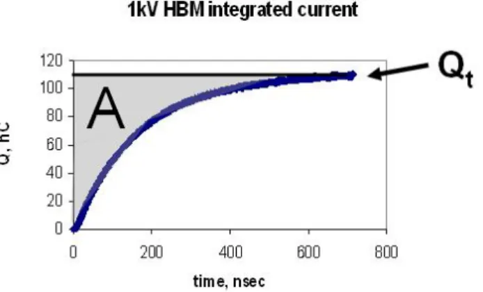
total charge Qt, and therefore C, are found by
integrating the current, the next integral gives us RC. Figure 9 shows the integrated 1kV HBM waveform as a starting point; the shaded area A gives RC when divided by Qt. This can be stated as
t t
corr t
Q
dt
d
h
Q
RC
∫
∫
∞
⎥
⎦
⎤
⎢
⎣
⎡
−
=
0 0τ
τ
)
(
. (28)
It is the Elmore Delay of the integrated HBM waveform. The result for the case in Fig. 9 was C=110 pF, R=1511 ohms, RC=166 nS. This is the same HBM waveform as above that gave 136.2 nS as the decay constant with the uncorrected current probe through standard methods. It now appears we can improve on those methods [15,16] so that we don’t span the entire 130-170 nS allowed range with the various alternatives. Digital oscilloscopes and ability to do this modest amount of data processing are now common enough to explore the methods outlined here.
Conclusions
We now can report first-order DUT transient information from TLP data, with a Z1(1+as) for each
pulse condition. This is done by considering the zeroth and first moments (integrals and centroids) of the waveforms or their derivatives, depending on whether short or long TLP pulses are used. This practice corresponds to “moment matching” of dc and first order transient response. The result is an equivalent series R+Ls or shunt admittance G+Cs, capturing voltage and current overshoot, respectively. The waveform moments are shown to be obtainable from successive waveform integration, with each
moment found as a dc offset, then removed and the process continued to find the next moment.
Figure 9: Integrated 0-ohm 1kV HBM waveform, showing convergence to total charge Qt=110 nC. The centroid of the
original waveform is its time constant RC=A/Qt., and here is also
the time at 63.2% of Qt, the expected result for 1-pole Elmore
Delay [6,10].
In this work, a circuit with a resistor plus ferrite bead was measured and characterized, with first order circuit models found sufficient to capture a 4-element model that operates at two distinct time scales.
We applied the same methods to formulate a circuit model for the transient behavior of a diode-triggered SCR as reported at this conference [9]. The linearized models are voltage/current dependent, as can be expected with semiconductor phenomena, but useful for circuit modeling and for capturing the essentials. The effect of finite rise time of a TLP system is often not negligible, particularly if the transients are on the same time scale as the TLP rise time. For example, the foregoing measurements and model extraction for ferrite bead and DTSCR would be somewhat enhanced by correcting for the TLP’s finite rise time. Often, even a one-pole model of the transient from TLP calibration data helps.
We also applied the same time-and-frequency domain Laplace transform methods to show how to correct HBM waveforms for droop in the CT-1 current transformer. The corrected waveform had closer to the expected decay constant value, and was also suitable for moment extraction and accurate measurement of the RC time constant and its constituents. The work explained much of why the HBM decay times come out lower than the expected 150 nS, while the actual RC is higher.
achieve this even more easily and are expected to help
with this activity in the future. [9] R. Gauthier, M. Abou-Khalil, K. Chatty, S. Mitra, and J. Li, "Investigation of Voltage Overshoots in Diode Triggered Silicon Controlled Rectifiers (DTSCR) Under Very Fast Transmission Line Pulsing (VFTLP)", 2009 EOS/ESD Proceedings (this meeting). Used with permission.
The lesson for all of us in this work is that TLP response is a step response, and results can be treated as an s-domain network function. With step response as our data, we are inspired to characterize our devices, circuits, and even measurement systems in a structured manner, using the many tools of network theory, time-and-frequency transformations, and their related approximation methods.
[10] H. Johnson and M. Graham, High Speed Signal Propagation, (Upper Saddle River, NJ:
Prentice-Hall, 2003), pp. 161-162.
[11] D. Tremouilles, et al., “Transient Voltage Overshoot in TLP Testing—Real or Artifact?”, 2005 EOS/ESD Symposium Proceedings, pp. 152-160.
Acknowledgements
The author thanks Arlene Wakita, John Dianda, and Bruce Chou for providing the TLP and HBM lab data.
He also thanks Robert Gauthier of IBM for Fig. 6. [12]http://en.wikipedia.org/wiki/Wiener_deconvolutioWeb article, “Wiener Deconvolution”;
n.
References
[1] T. Maloney and N. Khurana, "Transmission Line Pulsing Techniques for Circuit Modeling of ESD Phenomena", 1985 EOS/ESD Symposium Proceedings, pp. 49-54.
[13] N. Wiener, The Extrapolation, Interpolation, and Smoothing of Stationary Time Series with Engineering Applications (New York: Wiley,
1949).
[14] See, for example, “DSP” and “FIR filter” search items at http://www.tek.com.
[2] ANSI/ESD 5.5.1-2008 Standard Test Method for
TLP; ESD Association, Rome, NY. [15] ANSI-ESDSTM5.1-2007, “For Electrostatic
Discharge Sensitivity Testing--Human Body Model (HBM), Component Level”, ESD Association, 2007. See www.esda.org.
[3] ANSI/ESD SP5.5.2-2007 Standard Practice for Very Fast Transmission Line Pulse (VF-TLP). See www.esda.org.
[16] JEDEC JESD22-A114F standard,
“Electrostatic Discharge (ESD) Sensitivity Testing Human Body Model (HBM)”, Dec. 2008. See www.jedec.org.
[4] R.N. Bracewell, The Fourier Transform and Its Applications, (New York: McGraw-Hill, 1965).
[5] W.C. Elmore, “The Transient Analysis of Damped Linear Networks With Particular Regard to Wideband Amplifiers”, J. Appl. Phys. Vol. 19(1), pp. 55-63 (1948).
[17] Web articles,
http://mathworld.wolfram.com/PolynomialRoots. html, also
http://mathworld.wolfram.com/VietasFormulas.ht ml.
[6] R. Gupta, B. Tutuianu, and L.T. Pileggi, “The Elmore Delay as a Bound for RC Trees with Generalized Input Signals”, IEEE Trans. on Computer-Aided Design of Integrated Circuits and Systems, vol 16, no. 1, pp. 95-104, January 1997.
[7] M. Celik, L. Pileggi, and A. Odabasioglu, IC Interconnect Analysis, (New York: Kluwer
Academic Publishers, 2002).
[8] Web article, “Integration by Parts”;
http://en.wikipedia.org/wiki/Integration_by_parts.
[18] K. Verhaege, P. Roussel, G. Groeseneken, H. Maes, H. Gieser, C. Russ, P. Egger, X. Guggenmos, and F. Kuper, “Analysis of HBM ESD Testers and Specifications Using a 4th Order