SYNTHETICALLY CONTROLLING DOPING AND NANOSCALE MORPHOLOGY IN VAPOR-LIQUID-SOLID GROWN SILICON
NANOWIRES TO ENCODE FUNCTIONALITY
Joseph Dale Christesen
A dissertation submitted to the faculty at the University of North Carolina at Chapel Hill in partial fulfillment of the requirements for the degree of Doctor of Philosophy in the Department
of Chemistry in the College of Arts and Sciences.
Chapel Hill 2016
c
2016
ABSTRACT
Joseph Dale Christesen: Synthetically Controlling Doping and Nanoscale Morphology in Vapor-Liquid-Solid Grown Silicon Nanowires
to Encode Functionality
(Under the direction of James Cahoon)
Control of morphology and composition on nanometer length scales is a necessary tool for tuning the optical and electrical properties of semiconductor devices. Currently, this is achieved through “top-down” lithographic fabrication techniques, which are prohibitive due to high costs, increased complexity, and/or low throughput. Therefore, a new strategy is needed in order to create low cost and scalable method for fabricating nanomaterials for future semiconductor applications. Semiconductor nanowires (NWs) synthesized through the vapor-liquid-solid (VLS) mechanism are an ideal nanomaterial, as they enable rational synthetic control over composition, morphology, and corresponding properties of the NW from the atomic to microscopic scale.
ACKNOWLEDGMENTS
I would like to thank my entire family for all of their support. Words cannot express how thankful I am to my parents, Steve and Laurie, my brothers, Brien and Eric, my grandmother, Elaine, and all of my aunts, uncles, and cousins who helped motivate me over my five years of graduate school. I would also thank my wife, Sarah Christesen, for being with me for every step of this journey, and who’s support and understanding helped keep me going.
I would also like to thank my mentor and advisor Professor James F. Cahoon for five years of invaluable advice and guidance. I am thankful for his expertise, passion, and dedication to helping me grow and mature as a researcher. His encouragement and critiques pushed me to follow my dreams, and it allowed me to go beyond what I though I could ever accomplish during graduate school.
I would also like to thank all of the members of the Cahoon lab who were always willing to take time out of their day to help with experiments or answer any questions that I had about my project or science in general. Their support and encouragement pushed me to always better myself in my research, and I am truly grateful for all of their help.
TABLE OF CONTENTS
LIST OF FIGURES. . . xi
LIST OF TABLES . . . xiii
CHAPTER 1: INTRODUCTION . . . 1
1.1 Morphology Control in Semiconductors . . . 1
1.2 Semiconductor Nanowire Synthesis . . . 4
1.2.1 Heterostructures . . . 7
1.3 Properties of Semiconductor Nanowires . . . 9
1.3.1 Morphology . . . 13
CHAPTER 2: METHODS . . . 15
2.1 Nanowire Growth . . . 15
2.1.1 Substrate Preparation . . . 15
2.1.2 Nanowire Nucleation and Growth . . . 16
2.1.3 Epitaxial Shell Deposition . . . 17
2.3 Imaging and Analysis . . . 19
2.3.1 Scanning Electron Microscopy . . . 19
2.3.2 Transmission Electron Microscopy and Energy-Dispersive x-Ray Spectroscopy . . . 19
2.3.3 Fitting Diameter and Dopant Profiles . . . 20
2.4 Device Fabrication . . . 21
2.4.1 Marker Pattern Fabrication . . . 21
2.4.2 Nanowire Registration . . . 22
2.4.3 Nanowire Etching for Radial Photovoltaic Devices . . . 22
2.4.4 Evaporation of Metal Contacts . . . 22
2.4.5 Resistivity Measurements . . . 23
2.4.6 Photovoltaic Measurements . . . 24
2.5 Finite Element Simulations . . . 24
2.5.1 Optical Simulations . . . 24
2.5.2 Electrostatic Simulations . . . 25
CHAPTER 3: SYNTHETICALLY ENCODING 10 NM MORPHOLOGY IN SILICON NANOWIRES . . . 31
3.1 Introduction . . . 31
3.2 Methods . . . 33
3.4 Applications . . . 37
3.5 Conclusion . . . 41
CHAPTER 4: ENCODING ABRUPT AND UNIFORM DOPANT PROFILES IN VAPOR–LIQUID–SOLID NANOWIRES BY SUPPRESSING THE RESERVOIR EFFECT OF THE LIQUID CATALYST . . . 42
4.1 Introduction . . . 42
4.2 Results . . . 44
4.3 Kinetic Modeling and Analysis . . . 52
4.4 Conclusions . . . 60
CHAPTER 5: ROOM TEMPERATURE ELECTRONIC RATCHETS IN ANISOTROPIC SAWTOOTH SILICON NANOWIRES. . 62
5.1 Introduction . . . 62
5.2 Results . . . 64
5.3 Conclusion . . . 68
CHAPTER 6: DESIGN PRINCIPLES FOR PHOTOVOLTAIC DEVICES BASED ON SILICON NANOWIRES WITH AXIAL OR RADIAL P–N JUNTIONS . . . 69
6.1 Introduction . . . 69
6.2 Methods . . . 71
APPENDIX: CODE FOR IMAGE ANALYSIS . . . 89
LIST OF FIGURES
Figure 1.1: Si–Au binary phase diagram . . . 5
Figure 1.2: Schematic illustration of axial and radial NW heterostructures . . . 7
Figure 1.3: Methods for bottom-up control of NW morphology. . . 12
Figure 3.1: Synthesis of Si NWs with encoded morphology . . . 32
Figure 3.2: Characterization of NW growth, etching, and morphology. . . 34
Figure 3.3: SEM images and phosphine flow profiles for the synthesis of Si NWs with complex morphology . . . 36
Figure 3.4: Thermal Oxidation of ENGRAVE structures. . . 37
Figure 3.5: Nanogap-encoded NWs for plasmonics. . . 39
Figure 3.6: Nanorod-encoded NW for non-volatile memory . . . 40
Figure 4.1: VLS NW growth and the reservoir effect . . . 43
Figure 4.2: Characterization of P doping in VLS-grown Si NWs . . . 45
Figure 4.3: Fit of the EDS spectrum . . . 46
Figure 4.4: n-type Si NW resistivity measurements . . . 47
Figure 4.5: EDS spectrum, HAADF-STEM image, and EDS elemental images of a ntype/intrinsic/n-type segment. . . 49
Figure 4.8: Transition width at various carrier gas flow rates with a constant
NW growth rate . . . 53
Figure 4.9: Influence of NW growth rate and diameter on the abruptness of n-type/intrinsic dopant heterostructures . . . 57
Figure 4.10: Suppressing the reservoir effect for diameter-independent, high-resolution heterostructures . . . 60
Figure 5.1: Principles of geometric diodes and fabrication of sawtooth Si NWs . . . 63
Figure 5.2: Four-point probe measurements of geometric diodes . . . 66
Figure 6.1: Overview of NW geometries used for photovoltaics . . . 70
Figure 6.2: Details of simulation geometries used for finite-element modeling . . . 71
Figure 6.3: Charge density and electric field distributions for axial and radial NWs . . . 73
Figure 6.4: Depiction of the space-charge region in radial NWs at low doping levels . . . 74
Figure 6.5: Analysis of axial p–i–n junction photovoltaic device characteristics . . . 75
Figure 6.6: Analysis of radial p–i–n junction photovoltaic device characteristics . . . 78
Figure 6.7: Analysis of radial p–i–n junction photovoltaic device characteristics . . . 80
Figure 6.8: Comparison of simulated and experimental I–V or J–V curves for single-nanowire (NW) photovoltaics under 1 sun illumination . . . 82
Figure 6.9: Effective minority carrier diffusion length in axial NWs . . . 84
Figure 6.10: Photovoltaic performance of axial NWs at high doping levels . . . 85
LIST OF TABLES
Table 4.1: Encoded doping levels and measured active doping levels . . . 48
Table 6.1: Simulated photovoltaic metrics for axial NW p–i–n junctions . . . 76
Table 6.2: Simulated photovoltaic metrics for radial NW p–i–n junctions with
donor/acceptor doping levels of 1e18 . . . 79
Table 6.3: Simulated photovoltaic metrics for radial NW p–i–n junctions with
donor/acceptor doping levels of 1e20 . . . 79
Table 6.4: Comparison of experimental and simulated photovoltaic metrics for
LIST OF ABBREVIATIONS
2DEG two–dimensional electron gas
BHF buffered hydrofluoric acid
CVD chemical–vapor–deposition
EBL electron–beam lithography
EDS energy–dispersive x–ray spectroscopy
ENGRAVE Encoded Nanowire GRowth and Appearance through VLS and Etching
FF fill factor
FIB focused ion beam
ISC short–circuit current
IPA isopropyl alcohol
IQE internal quantum efficiency
IR infrared
JSC short–circuit current density
Leff effective minority carrier diffusion length
LED light-emitting diode
MIBK methyl isobutyl ketone
MMA methyl methacrylate
NPGS Nanometer Pattern Generation System
NW nanowire
PML perfectly matched layer
PMMA polymethyl methacrylate
QD quantum dot
sccm standard cubic centimeters per minute
SEM scanning electron microscope
SERS surface–enhanced Raman spectroscopy
SOI silicon–on–insulator
SPP surface plasmon polariton
SRH Shockley–Read–Hall
SRV surface recombination velocity
STEM scanning transmission electron microscope
TEM transmission electron microscope
VLS vapor–liquid–solid
VS vapor–solid
VSS vapor–solid–solid
WZ wurtzite
CHAPTER 1: INTRODUCTION
1.1 Morphology Control in Semiconductors
Since the discovery of semiconductors, control of morphology and composition has been a necessary tool in tuning the optical and electrical properties of devices. Control of doping and pattering of Si in particular enabled the departure from vacuum tube to the solid state transistor, which ushered in the digital age.1 As the control of doping and pattering increased, so did the
quality and quantity of the transistors.2 The technology for controlling the morphology and composition improved at such a rate that Gordon Moore famously predicted, "The complexity for minimum component costs has increased at a rate of roughly a factor of two per year. Certainly over the short term this rate can be expected to continue, if not to increase. Over the longer term, the rate of increase is a bit more uncertain, although there is no reason to believe it will not remain nearly constant for at least ten years."3 Moore’s law, as it is generally referred to, continued not just for the ten years that Gordon Moore predicted, but for over fifty years.
electrical components. The resolution at which the photomask can be transferred to the photo resist is generally limited by the Abbe diffraction limit, which can be written as
d= λ
2nsinθ (1.1)
where λis the wavelength of light,θ is the angle of incidence, nis the refractive index, anddis the spot size. Therefore, the resolution can be improved by either decreasing the wavelength or increasing the denominator,nsinθ, which is generally referred to as the numerical aperture. This has led to lithographic techniques such as extreme ultraviolet, immersion, and phase shift lithography in an attempt to improve the resolution of photolithography beyond the diffraction limit.4–7 While these techniques can improve the resolution down to tens of nanometers, they
become increasingly more complex, difficult, and/or cost prohibitive to manufacture and utilize in various nanotechnology applications.
tures due to high costs, increased complexity, and/or low throughput, and therefore, a new strategy is needed in order to create low cost and scalable method for creating nanomaterials for future semiconductor applications. Significant research has been devoted to the "bottom-up" chemical synthesis of semiconductor nanostructures, and this paradigm offers a scalable method for creating nanostructures with atomic precision and distinct composition, size, and morphology.
These semiconductor nanostructures are generally categorized based on the number of non-nanoscale dimensions the structure posses. 0-D structures, or quantum dots (QDs), are structures in which all three dimensions are in the nanoscale, and they have been synthesized with a wide variety of shapes, sizes, and compositions.10,11 Solution based synthesis methods are the most common for QDs, and they allow for precise control of size and composition and is readily scalable to various manufacturing processes including roll-to-roll printing.12 QDs are usually only a few nanometers in size, which gives rise to quantum confinement effects and including size dependent photoluminescence.10 These quantum effects have been studied for various applications in photonics and electronics including lighting and photovoltaics.13–15 While the quantum mechanical description for the semiconductor dot is well understood, a significant amount of research has been devoted to understanding the chemistry and electron kinetics of the solution interface of QD as well as transfer of electrons between QDs, which is necessary for future applications where electronic connection between QDs is paramount.16,17
transistor in electronic applications.19 Other 2-D materials have been studied for applications in transistor electronics as well as photonics including transition metal dichalcongenides, which have band gaps ranging from the UV to the infrared (IR) .20 However, most methods for synthesizing
these 2D materials require separating bulk material into individual sheets though mechanical or chemical means, and therefore, it lacks precise control of composition as well as geometry though research is currently progressing on addressing these issues.
1-D structures, or NWs, are high aspect ratio nanomaterials in which only two dimensions are nanoscale, and they have become one of the most powerful tools for nanoscience. Through semiconductor NWs, it is possible to ab initio design and synthetically tune the composition, morphology, and corresponding properties of the NW from the atomic to microscopic scale. This level of control makes NWs an ideal nanomaterial building block, enabling a wide variety of new technologies as well as improvements on previous technologies, and will be the focus of this dissertation.
1.2 Semiconductor Nanowire Synthesis
Figure 1.1: Si–Au binary phase diagram.
More Si precursor is continually introduced into the system such that the alloy concentration moves toward continually increasing Si concentration until no solid Au remains, and the particle is a complete liquid droplet. The liquid alloy is pushed out of equilibrium by the continual incorporation of the Si precursor into the liquid droplet, and eventually, the liquid droplet crystallizes solid Si in an area defined by the size of the original Au nanoparticle. Therefore, the size of the initial Au catalyst determines the final diameter of the Si NW.
For many applications of VLS grown NWs, it is necessary to grow NWs with a high level of precision over parameters such as diameter, crystallinity, crystal direction, and uniformity. Therefore, it is crucial to understand key factors of NW growth via the VLS mechanism in order to synthetically control crystal direction, crystal defects, kinking, and overcoating. Crystal defects such as twin planes,24–27 stacking faults,25 and screw dislocations28–30 are know to
affect the growth morphology as well as optical31 and electronic properties32 of NWs and can be controlled through a wide variety of synthetic parameters including gas flow rates,30 temperature,25 and surface chemistry.24 Twin planes and stacking faults can occur in group
crystal defects can also lead to mixtures of wurtzite (WZ) and zincblende (ZB) crystal structures generally in III–V semiconductor NWs and can be controlled through a combination of NW diameter and temperature.25 The WZ and ZB crystal structures have different band gaps and
can even switch between direct and indirect-band gaps in certain materials.35
Figure 1.2: Schematic illustration of a (A) VLS growth of a homogeneous NW, and the subsequent formation of heterostructures from (B) continued VLS growth or (C) VS growth.
promote stable growth.46,49–51 The surface adsorbate used are atoms or small molecules (i.e. H46, Cl51, CH346,49,50) that will readily adsorb to the NW and prevent any reactions of the precursor gas with the NW surface.
1.2.1 Heterostructures
The true power of NWs is the ability to tune structure and composition on a variety of length scales ranging from single atoms to microns, which is due in part to the wide variety of materials that are compatible with VLS mechanism. It is these heterostructures that enable breakthroughs and advances in technology. The ability to modulate composition both axially and radially with respect to the NW growth direction as schematically depicted in Figure 1.2 allows for synthetic control of diverse set of properties including band gap, Fermi level, crystal structure, dielectric constant, modulus, thermal conductance, mobility, carrier concentration, and many others.
simultaneously incorporating a new material. Because of the time necessary to completely switch the materials in the catalyst, the demarcation between the two materials in the solid NW will be blurred in what is commonly know as the "reservoir effect" in the NW literature. This effect has been observed for heterostructures involving a change in dopants (e.g., P-doped Si52 and Si-doped GaAs57) and structures involving a change in semiconductor (e.g., Si/Ge58–60 and GaAs/InAs61,62). For group IV NWs, transition widths comparable to the wire diameter have
been observed for P dopant transitions52 as well as junctions between Si and Ge.58–60Several strategies to mitigate this effect have been developed. For example, metal catalysts with a lower solubility of semiconductor in the liquid, such as an Au1−xGax alloy,63can shorten the transition
width. Another alternative is to forego the VLS mechanism in favor of a vapor–solid–solid (VSS) mechanism, in which the metal catalyst is solid and has little to no solubility with the semiconductor.64,65 The VSS growth process has been successfully demonstrated for dopant transitions in Au-catalyzed NWs66and for Si/Ge transitions in AuAl-catalyzed NWs.65Although VSS growth has been shown to produce near-atomic compositional transitions, the growth rate is slow, preventing application for many devices. For III–V NWs, the reservoir effect has been observed for heterostructures involving a change in dopant and a change in the group III material.58 However, the effect is generally not observed for a change in the group V material, which has been attributed to the low solubility of group V elements in the liquid catalyst.63 For structures in which the group III material is changed, methods such as pulsing the group III precursor have improved the transition width, resulting, for example, in sharper InAs/GaAs transitions.67 In this case, it is believed that Ga reduces the solubility of In in the metal catalyst to reduce the reservoir effect; however, a general strategy for suppression of the effect has yet to be developed.
heterostruc-tures as depicted in Figure 1.1C unlike the unintended, amorphous VS overcoating previously described. By increasing the temperature well above the eutectic temperature and lowering the partial pressure of reactant gasses, the VLS mechanism is suppressed, and overcoating via the VS mechanism is greatly enhanced. The high temperatures also facilitates the formation of an epitaxial crystalline shell on the NW. The radial structures do not have the problem of the reservoir effect because the heterostructure formation does not go through the catalyst. However, at elevated temperatures, there is the possibility of diffusion of materials in the NW, but atomically abrupt heterostructures are possible.
1.3 Properties of Semiconductor Nanowires
NWs exhibit unique optical, electrical, and mechanical properties due to their geometry as well as compositional variation within said geometry. With control over these properties along a single NW, one has the building blocks necessary to create devices for new technologies, and we will discuss these unique properties and how they can be applied to various technologies and devices.
NWs have generated a lot of interest for electronics applications due to the precise band-gap engineering and new devices geometries.68 Because NWs are synthesized from the bottom-up, it is much easier to control the band-gap, Fermi level, and carrier concentrations through doping or material changes. This allows for fabrication of abrupt69 or graded70 heterostructures or thin barriers for quantum applications including single electron transistors71 or resonant-tunneling diodes.72
part due to its low cost, and the inability to reliably fabricate other semiconductors off of silicon– on–insulator (SOI) substrates due to large crystal mismatches. The NW geometry, however, allows for heterostructures between crystals with widely varying lattice constants because the strain can be relaxed at the edge of the NW. Therefore, NWs can be grown epitaxially off of SOI substrates, which makes it a promising candidate for integrating other higher mobility materials with current architectures.
Similar to the precise electronic control, NWs can also be fabricated with control over optical properties such as the type and size of the band gap and refractive index, which makes NWs an attractive building block for light management applications such as light-emitting diodes (LEDs), lasers, single-photon sources, and photodiodes.73,74 Altering the band gap for tuning the emission of NWs has enabled the fabrication of LEDs with tunable emission from the UV to the IR in a manner not possible with planar technology.75 Phosphor-free white LEDs have been produced in InGaN/GaN NWs by tuning the length and composition of the InGaN quantum well segments, which is not possible in planar technology due to the quantum confined Stark effect.76 NWs can also be fabricated into lasers where the NW defines both the lasing cavity and gain material. The compact footprint of NWs make them promising candidates for applications where current laser sources cannot be used such as optical on-chip communication and in situ biodetection.77–79 The synthetic variety of NWs allows for tunability in cavity and the gain medium, and NWs lasers have already been demonstrated with wavelengths ranging from the UV all the way out to the IR and have been pumped both optically and electronically.77–79
inefficient extraction of photons decreases the overall efficiency of the device. QDs embedded in axial or radial NW heterostructures are a promising candidate due to the high extraction efficiencies provided by the NW scaffold.80
Because of their subwavelength size, NWs can generate strong resonances based on their cross-sectional shape and size.81–83These resonance modes lead to greatly enhanced light-matter interactions and longer effective absorption path lengths along in the NW. This coupled with low leakage currents in axial p-n junctions makes NWs a promising candidate for wavelength selective avalanche photodiodes.84,85
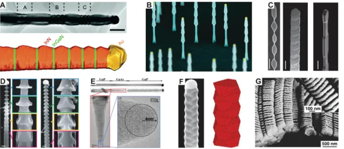
Figure 1.3: Methods for bottom-up control of NW morphology. (A) Diameter modulation of III–V VLS-grown NWs; scale bar, 100 nm. (B) Chemically controlled VS sidewall deposition on Ge NWs. (C) High-temperature shell deposition on Si NWs showing periodicity as a result of Plateau–Raleigh instability; scale bars, 400 nm. (D) Si NWs with Au silicide that acts as an etch stop for aqueous KOH etching; scale bars, 200 nm. (E) GaAs/ GaP NWs etched in aqueous KOH solution. (F) Twinning super lattice in InP NWs. (G) Au NWs with gaps produced by on-wire lithography (OWL). Reprinted with permission from Christesen, J. D., Pinion, C. W., Hill, D. J., Kim, S. & Cahoon, J. F. Chemically Engraving Semiconductor Nanowires: Using Three-Dimensional Nanoscale Morphology to Encode Functionality from the Bottom Up. J. Phys. Chem. Lett. 2016,7, 685–692. Copyright 2015 American Chemical Society.
1.3.1 Morphology
The NW geometry offers a platform for nanometer-scale morphological control, and significant research effort has been devoted toward controlling the morphology of wires grown by VLS mechanism.25,49,50,89–98For example, the Gradecak research group at MIT modulated the diameter of III–V NW catalysts by altering the catalyst supersaturation, allowing an ∼25% modulation of the NW diameter (Figure 1.3A) during VLS growth.91 Because the morphology change is
Northwestern University developed a method termed on-wire lithography (OWL) for creating nanometer-sized gaps in metal NWs (Figure 1.3G).99 The NWs are grown via electro-deposition into a porous substrate, and the deposited material can be altered during growth. Following growth, the porous substrate is removed and the material is etched, leaving gaps less than 5 nm in length. Other template-assisted growth mechanisms, such as coaxial lithography100 (COAL) and template-assisted selective epitaxy101 (TASE), have also been developed to create complex
CHAPTER 2: METHODS
2.1 Nanowire Growth
Si NWs were grown with a home-built, hot-wall chemical–vapor–deposition (CVD) system, which consists of a quartz tube furnace (Lindberg Blue M) with 1 inch diameter bore, fast-responding mass-flow controllers (MKS Instruments P4B), a pressure control system (MKS Instruments 250E), and vacuum system with base pressure of < 2×10⁻³ Torr. The CVD system was computer-controlled using custom Labview software to enable rapid and reproducible modulation of the NW growth conditions and gas flow rates. The NWs are grown using Au nanoparticles dispersed onto a silicon-silicon oxide substrate within a 1 inch outer diameter quartz tube (Chemglass Life Sciences).
2.1.1 Substrate Preparation
for another 5 minutes at a temperature of 150 ◦C. The last UV-Ozone cleaning is performed within 6 hours of growth to remove any remaining carbon species from the substrate. Before the wafer is inserted into the quartz tube, the quartz tube is heated to 950 ◦C for 1 hour under 20 sccm of Ar flow to remove any excess material or contaminates from the tube surface. The quartz tube is allowed to cool down to a temperature∼100◦C below the initial run temperature, and the wafer is then inserted into the quartz tube within the single-zone quartz tube furnace, such that the substrate is directly above the K-type thermocouple. The system is pumped down to a base pressure of<2×10⁻³ Torr, heated to the starting temperature, and allowed to settle before the run is started.
2.1.2 Nanowire Nucleation and Growth
NWs are nucleated at a furnace temperature between 420 ◦C and 460 ◦C, a total reactor pressure of between 20 and 100 Torr, a carrier gas flow of between 10 and 200 standard cubic centimeters per minute (sccm) of either H2 (Matheson Tri-Gas; 5N semiconductor grade) or Ar (Matheson Tri-Gas; 5N semiconductor grade), a SiH4 (Voltaix) flow rate of between 0.5 and 2 sccm, and optionally dopant flows of between 0.15 and 20 sccm of either PH3 (Voltaix; 1,000 ppm in H2) or B2H6 (Voltaix; 100 ppm in H2) for between 5 and 30 minutes.
2.1.3 Epitaxial Shell Deposition
Growth of an epitaxial shell is performed directly after the completion of the axial growth of the NW. The chamber is evacuated to its base pressure, and the furnace is then heated to 760
◦C with 0.15 sccm of SiH
4 at 25 Torr without breaking vacuum in order to prevent any oxide formation on the NWs. The SiH4 flow rate is set to its minimum to prevent supersaturation of the catalyst and continued VLS growth. To encode an n-type shell, 0.75 sccm of PH3 is added. The calibrated shell growth rate under these conditions is ∼1.5–2 nm/min.
2.1.4 Oxidation
Thermal oxidation treatments can be performed in order to passivate surfaces102 or effect doping levels in Si.103–106 After the CVD growth is over, NWs were removed from the CVD system, and loaded into another quartz tube furnace (Lindberg Blue M) with three separately controllable temperature zones and a 5 inch diameter bore. The substrate was placed in a quartz boat that remains outside of the furnace while the furnace is heated to temperature. The quartz boat is attached to a quartz rod containing a magnet sealed inside of it at the far end, which allows rapid insertion into the furnace and prevents oxidation of the magnet. The system is pumped down to base pressure and the first zone is heated to 1000◦C. O2 is then introduced at 20 sccm and the system is pressurized to 100 Torr of pure O2. The substrate and the quartz boat are inserted into the furnace by using an external magnet to slide the whole assembly in side the tube. The NWs are then oxidized for a time from 1 to 20 min, and the external magnet is used to quickly remove the sample from the furnace. The system is then evacuated to its base pressure before pressurizing with Ar and removing the sample.
2.2 Wet-chemical Etching
For wet-chemical etching, NWs were mechanically transferred from the growth substrates onto Si wafers coated with 100 nm thermal oxide and 200 nm Si nitride (Nova Electronic Materials). The native oxide of the NWs, which were lying flat on the substrate, was etched by immersing the substrate in concentrated buffered hydrofluoric acid (BHF) (Transense BHF Improved) for 10 s. The substrate was then rinsed in nanopure water twice for 10 seconds each and in IPA for 30 seconds. The IPA was kept at the same temperature as the etch solution to allow the temperature of the substrate to equilibrate before inserting it into the etch solution. The substrate was then inserted into the KOH-etching solution (20.0 g KOH; 80.0 g water; 20 mL IPA as top surface layer) at a temperature between 20 and 40◦C for variable times up to 200 s. The substrate is then rinsed in a slightly acidic solution (∼4% acetic acid in water) to quench the etching process for 10 s, in nanopure water for 10 s, and in IPA for 15 s before drying with nitrogen. It was also noted that for NW transferred onto a marker pattern (see Chapter 2.4.1) the etch rate increased by ∼20-30%.
For NWs grown with significant Au diffusion along the side walls, the Au will act as an etch stop. An Au-etch step can be performed to remove any Au from the surface and can produce better etch results. For Au etching, the substrate is immersed in an Au etching solution (4 g KI; 1 g I2; 40 mL H2O) for 15 seconds, rinsed in nanopure water twice for 10 seconds each, rinsed in IPA for 15 seconds, and blown dry with nitrogen. The wet-chemical etching of the NWs can be performed directly after the Au etch by skipping the IPA rinse and drying steps, inserting the substrate directly into the BHF solution, and following the previously described etch steps.
to remove any excess BHF from the sample and allow the KOH to penetrate the NW mesh. Without vigorous shaking, BHF is not completely rinsed, and it will continue to etch the n-type regions through the remaining steps of the etching procedure. The etching of the n-type regions will be nonconformal and porous. It was also noted that the etch rate on the growth substrates was higher than mechanically transferred NWs by∼50% and that growth substrates with a lower density of NWs produced more conformal etching.
2.3 Imaging and Analysis
2.3.1 Scanning Electron Microscopy
Scanning electron microscope (SEM) imaging was performed with an FEI Helios 600 Nanolab Dual Beam system with an imaging resolution <5 nm using a typical acceleration voltage of 5 kV, imaging current of 86 pA, and a working distance of∼4 mm.
2.3.2 Transmission Electron Microscopy and Energy-Dispersive x-Ray Spectroscopy
EDS maps. STEM images were obtained before and after map acquisition to note any change in the sample.
2.3.3 Fitting Diameter and Dopant Profiles
Diameter profiles were obtained from analysis of SEM images using custom program in MATLAB as seen in Appendix . The program first uses the scale bar to identify the scale of each pixel in the image. The user then identifies the orientation of the NW in order for the program to rotate the NW to vertical. Each pixel of the SEM image is then binned based on their intensity values into three separate bins. The diameter is then calculated by scanning across the NW, identifying the position of the two NW edges based on the binned values of each pixel, and calculating the distance between them over the entire length of the NW.
In order to calculate the transition width between n-type and intrinsic segments of NWs, the diameter profiles were fit to a Gaussian convoluted with an exponential. The exponential is used to account for the "reservoir effect", and the convolution of the Gaussian is used to correct for limits of the etching procedure due to mass transport. The equation for a Gaussian convoluted with an exponential used to fit the experimental data is:
f(t) =cA∗exp
−(t−ct0)∗λa−σa2
σ2
a
∗erf
"√
2∗(t−ct0)∗λa−σa2
(2∗σa∗λa) + 1
#
−cA∗ "
1 +erf "√
2∗(t−ct0)
2∗σa
##
+cA∗erf
t−ct1 λb
+cI1 (2.1)
where cA is the radius of the NW, ct0 is the location of the n-type/intrinsic transition, ct1 is the location of the intrinsic/n-type transition, σa is the Gaussian broadening, λa is the
transition width of the n-type/intrinsic transition,λbis the transition width of the intrinsic/n-type
2.4 Device Fabrication
2.4.1 Marker Pattern Fabrication
Marker patterns were generated using the Nanometer Pattern Generation System (NPGS) system, which is an EBL system, on a Hitachi S4700 Field Emission SEM to precisely identify NW locations in order to make electrical contacts to individual NWs. A Si wafer with a 200 nm Si nitride (Nova Electronic Materials) layer on top was cleaned by sonicating in acetone, rinsing with acetone and IPA, and inserted into a UV-Ozone cleaner for 5 minutes at 150◦C. Two spacer layers of methyl methacrylate (MMA) (MicroChem MMA (8.5) MMA EL 9) were dispersed using a spin coater (Laurell Technologies Model WS-650-23B) onto the cleaned substrate at 4000 rpm for 30 s, and baked at 180◦C for 1 minute after each layer. A final photoresist layer of polymethyl methacrylate (PMMA) (MicroChem 950 PMMA A2) was applied under the same conditions and again baked at 180◦C for 1 minute. The marker pattern was then written with the NPGS system at a working distance of 25 mm, current of 400 pA, and a magnification of 100×for the inner pattern and a working distance of 25 mm, a current of 7 nA, and a magnification of 20×for the outer pattern. The substrate is then developed in methyl isobutyl ketone (MIBK)
2.4.2 Nanowire Registration
NWs are then transferred to the marker pattern through mechanical transfer. Two layers of MMA and one layer of PMMA are applied using the same procedure describe before for marker pattern fabrication. Images of the maker pattern are taken using a Zeiss HAL 100 halogen lamp installed on a Zeiss AxioImager A2M upright microscope. A 10x objective with a numerical aperture of 0.2 and a working distance of 14.3 mm (Zeiss EC Epiplan 10x/0.2 HD WD = 14.3 M27) was used for low-magnification images, and a 50x objective with a numerical aperture of 0.75 and a working distance of 1.0 mm (Zeiss EC Epiplan 100x/0.75 HD WD = 1 M27) was used for high-magnification images. The locations of the NWs on the marker pattern were then registered using custom software in Igor, and contacts were drawn to the NWs in the DesignCAD file. After the sample is loaded into the SEM, NPGS is used to identify a transformation matix for the underlying maker pattern relative to the SEM image. Using the transformation matix, the inner contacts were written at a working distance of 25 mm, a current of 400 pA, and a magnification of 100x, and the outer contacts were written at a working distance of 25 mm, a current of 7 nA, and a magnification of 20x.
2.4.3 Nanowire Etching for Radial Photovoltaic Devices
For radial photovoltaic devices, SU-8 photoresist (MicroChem, 2000.5) was patterned by Xing Zhang on 15–30 µm-long portions of the NWs using EBL followed by wet chemical etching with KOH solution (18 g in 60/20 mL water/IPA at 60 ◦C) to remove the intrinsic and n-type shells in regions of the NWs not covered with resist in order to make electrical contact to the p-type core. SU-8 photoresist was subsequently removed using a UV-Ozone cleaner.
2.4.4 Evaporation of Metal Contacts
water rinses for 10 s each, and an IPA rinse for 15 s before drying the sample with nitrogen. This etch is to remove any oxide on the NWs to ensure good contact between the metal and the NWs. Oxide will start to form on the NWs after BHF etching, and therefore, it is imperative to load the sample directly after etching and rinsing to prevent a substantial oxide buildup. Contacts are evaporated using Ti and Pd at pressures of<1×10⁻⁷ Torr. To lower the pressure below 1×10⁻⁷ Torr, Ti and Pd are first degassed as previously described for Cr and Au, and then Ti is evaporated with the shutter closed to getter remaining gaseous species in the chamber. Ti is evaporated at a rate of 0.2 Å/s for 3 nm, and Pd is evaporated for 0.2 Å/s for the first 10 nm, 0.5 Å/s for the next 40 nm, and 1.0 Å/s until the total thickness is 50 nm larger than the NW diameter. The substrate is removed from the chamber, and the resist is dissolved in acetone to remove all excess metal.
2.4.5 Resistivity Measurements
2.4.6 Photovoltaic Measurements
Dark current–voltage (I–V) curves were measured by Xing Zang and Christopher Pinion using a Keithley 2636A SourceMeter in conjunction with Signatone micropositioners (S-725) and probe tips (SE-TL). I–V curves under 1-sun illumination were also measured by Xing Zang and Christopher Pinion with the same SourceMeter and with metal contacts formed using a wire bonder (West Bond model 7476D) with 1% Si/Al wire. The solar simulator used for light measurements (Newport, model 91191 with 1 kW Xenon lamp) contained an AM1.5G filter and was calibrated to 1-sun (100 mW/cm2) using a calibrated reference solar cell (Newport, model 91150V). After measurement, NW diameters and lengths were determined by high resolution SEM.
2.5 Finite Element Simulations
Both optical and electrostatic finite element simulations were performed using the Comsol Multiphysics commercial software package. Comsol Multiphysics is a finite element analysis, simulation, and solver software package, which enables simulation of a wide variety of systems through inclusion of relevant physics modules. Modules used for optical and electrical simulations include the AC/DC, transport of dilute species, and electrostatics modules.
2.5.1 Optical Simulations
Figure 3.5) were generated by evaluating the scattered electric field intensity (|E|2) in a horizontal plane 3 nm above the top surface of the NW.
2.5.2 Electrostatic Simulations
Electrostatic finite-element simulations were used to evaluate photovoltaic as well as phase change memory devices. These simulations used cylindrical symmetry to represent the three-dimensional structure. For both simulations, the external voltage was applied to Ohmic contacts on the n-type regions, and the simulations included realistic doping profiles as well as drift-diffusion physics. Simulations of the photovoltaic devices also include recombination processes to reproduce the current–voltage characteristics of the devices.
For the simulations of photovoltaic devices, the physics is based on the standard semiconductor drift and diffusion model107,108 in which the electron continuity equation is represented as:
dn
dt =∇ ·(Dn∇n−µnnE)−R+G= 0 (2.2)
wherenrepresents the concentration of electrons,ttime,Dnthe electron diffusion constant,µnthe
electron drift mobility,Ethe internal electric field,Rthe net rate of charge-carrier recombination, andG the optical generation rate of charge carriers. The corresponding equation for holes,p, is given by the analogous equation with substitution of pforn. The electric field,E, is determined by Poisson’s equation, which relatesE to the electric potential,ψ, and the charge densityρ as:
ε∇E=−εrε0∇2ψ=ρ (2.3)
ρ=q(Nd−N a−n+p) (2.4)
where Nd and Na are the density of donor and acceptor atoms, respectively, and q is the
elementary charge. The spatial distributions of the donor and acceptor regions are represented as: N =
Nd,0+Na,0exp
−12(x−xa∆x )2 (x < xd)
Nd,0exp
−12(x−xd∆x )2+Na,0exp
−12(x−xa∆x )2 (xd≤x≤xa)
Na,0+Nd,0exp
−1 2(
x−xd
∆x )2
(xa< x)
(2.5)
whereNd,0andNa,0are the maximum donor and acceptor densities,xdandxaare the boundaries
of the heavily doped donor and acceptor regions, respectively, andx is the width of the dopant transition as represented by a half-Gaussian function. Note that xd < xa, the length of the
intrinsic region is estimated as xa -xd, andx represents the radial direction in radial devices
and the axial direction in axial devices.
Because of the high doping levels used in NW devices, the mobility values are dependent upon the doping level as given by the empirical relationships:109
µn= 92
cm2
V ·s+ 1268 "
1 +
Na+Nd
1.3×1017cm−3
0.91#−1 cm2
V ·s (2.6)
and
µp = 54.3
cm2
V ·s+ 406.9 "
1 +
Na+Nd
2.35×1017cm−3
0.88#−1 cm2
V ·s (2.7)
mobility through the Einstein relation:
D= kT
q µ (2.8)
where k is Boltzmann’s constant, and T is temperature in Kelvin. The bandgap of Si also depends on doping as a result of bandgap renormalization; the shift in bandgap can be described empirically as:107,109
∆Egap=−0.0187
ln
Nd
7×1017cm−3
+ln
Na
7×1017cm−3
eV (2.9)
which is valid for |Nd−Na|>7×1017cm−3. The bandgap of silicon is thus given as:
Egap=Egap,0−∆Egap (2.10)
whereEgap,0 is the non-degenerate bandgap of 1.12 eV.
For calculation of the p–n junction characteristics under equilibrium conditions at zero external applied voltage, the built-in potential,ψbi, is fixed between the Ohmic contacts. In the
absence of degenerate doping (Na;Nd<1017 cm−3), the built-in potential can be represented as:
ψbi,0= kT
q ln
NaNd
n2
i,0 !
(2.11)
Where Nc andNv represent the conduction and valence band density of states with values of
2.86×10¹⁹and 2.66x1019cm−3, respectively, andEgap is the doping-level dependent bandgap
given in equation 2.10. For degenerate doping, the standard approximation for the Fermi level, EF, which assumesEF is >3kT from the band edge and is implicit in equation 2.11, substantially
deviates from the true value, so we instead use the Joyce-Dixon approximation110 to estimate the difference between EF and the band edge:
∆EJ D,c=EF −Ec=
kT q ln Nd Nc +√1
8 Nd Nc − 3 16 − √ 3 9 ! Nd Nc 2! (2.13)
whereEcis the energy of the conduction band edge. An analogous expression can be written for
the valence band substituting in Nv, Na, and Ev, the energy of the valence band edge. Based on
this approximation, we introduce a correction term for the built-in voltage as:
∆Ecorrection=Egap,0+ ∆EJ D,c+ ∆EJ D,v−ψbi,0 (2.14)
We can thus represent the final built-in voltage as:
ψbi=
kT q ln
NaNd
ni,ani,d
+ ∆Ecorrection+
∆Egap,0
2 (2.15)
The potential applied between the Ohmic n-type and p-type contacts, ψ,is given by:
ψ=ψbi+Vapplied (2.16)
where Vapplied is the external voltage applied to the p-type Ohmic contact such that a positive
To model current–voltage characteristics of the p–n junctions, the recombination term Rin equation 2.2 includes Shockley–Read–Hall (SRH)107,108 as:
RSRH =
np−n2i
τn(p+ni) +τp(n+ni)
(2.17)
where τn andτp represent the minority carrier lifetimes for electrons and holes, respectively. For
all simulations we set these lifetimes equal so that τn=τp =τ. Where noted in the text, the
recombination termR also includes Auger recombination107,108 as:
RAuger =
n(np−n2
i) τA,nN2
d
f orNd>5×10¹⁵
p(np−n2
i) τA,pN2
a f orNa>5×10
15
(2.18)
where the Auger lifetimes, τA,n and τA,p, are given in the low-injection regime by:111
τA,n=
1 1.8×10⁻²⁴cm−3(N
d)1.65
s (2.19)
and
τA,p =
1 6×10⁻²⁵cm−3(N
d)1.65
s (2.20)
The simulations include surface recombination as a boundary condition on the outer surfaces of the simulation domain excluding the Ohmic contacts. The rate of surface recombination is calculated as:107,108
RS =
np−n2i
Sn−1(p+ni) +Sp−1(n+ni)
CHAPTER 3: SYNTHETICALLY ENCODING 10 NM MORPHOLOGY IN SILICON NANOWIRES1
3.1 Introduction
Most semiconductor technologies rely on the ability to pattern materials with nanometer-scale features using top-down lithographic tools. Over the last decade, however, bottom-up chemical methods to control the size, shape, and composition of nanoscale materials have progressed rapidly, resulting in a diverse set of well-controlled morphologies including dots, rods, ribbons, and wires.112–114 Semiconductor nanowires (NWs) are recognized as an especially important technological building block because the high aspect ratio can be used for longitudinal transport of electrical or optical signals.112,113 A variety of devices have been demonstrated, including sensors,115 waveguides,116 phase-change memory,117 light-emitting diodes,118 and solar cells.83,119,120 Nevertheless, current NW-based technology has been limited by the material’s translational symmetry and the inability to pattern arbitrary, nanometer-scale morphological features.
NWs are typically synthesized using the VLS mechanism,21 in which a metal nanoparticle catalyzes one-dimensional growth of a single-crystalline semiconductor material. Advancements in VLS-based technologies have generally involved synthesis of new materials or heterostructures.121 For instance, NW superlattices, in which the composition of a NW is modulated along the growth axis, have been reported for Si/SiGe,59 GaAs/GaP,69 InAs/InP,122,123 Zn-doped InP,27
1
CdSe/ZnSe,124 and P-doped Si.125 Modulation of NW composition often results in faceting of the NW surface, providing some capability to control morphology during synthesis.25,27,98,123 In addition, NW superstructures have been reported in the form of controllably kinked NWs that break the one-dimensional shape.39,126 Nevertheless, only a handful of reports describe efforts to alter the NW geometry and encode specific morphology. For example, controlled VS over-coating on the NW surface has been used to create tapered structures127 and periodic variations in
morphology.50 In addition, modulation of the size of the metal catalyst during growth has been shown to provide control over the NW diameter.91,92 For metal NWs, electrodeposition in metal oxide templates followed by wet-chemical etching has been used to create wires with alternating, nanoscale structures.99,128 However, a method for accurate, nanometer-scale control of morphology in single-crystalline semiconductor NWs has not been developed. Here, we demonstrate a new method to achieve this type of high-fidelity shape control, a process which we term Encoded Nanowire GRowth and Appearance through VLS and Etching (ENGRAVE). The key aspects and capabilities of this method are illustrated in Figure 3.1 and elaborated below.
3.2 Methods
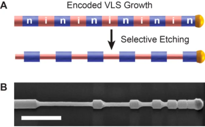
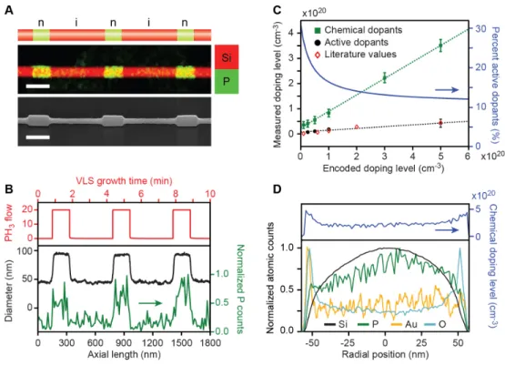
Si NWs were grown by a VLS mechanism in a home-built, hot-wall chemical vapor deposition (CVD) system at 420◦C using Au nanoparticles as catalysts, silane (SiH4) as the source of Si, and hydrogen (H2) as the carrier gas (see Chapter 2.1 for details). As illustrated schematically in Figure 3.1A, an additional flow of phosphine (PH3) was rapidly modulated during growth125 to encode varying levels of P, an n-type substitutional dopant with high solubility in Si.129–131 The
etch rate of doped Si with aqueous KOH solution is well-known to decrease with higher dopant concentration.132 This effect has been observed in doped Si NWs, producing changes in diameter along the axis.66,133 Here, we develop this effect as a tool to encode arbitrary, high-resolution morphology along the NW growth axis, enabling new technological applications of Si NWs. 3.3 Characterization and Optimization of ENGRAVE
To delineate the spatial resolution of the ENGRAVE process, we synthesized NWs with six intrinsic segments encoded along the axis for increasingly short time scales. As shown in Figure 3.1B, wet-chemical etching of these segments yielded an abrupt and conformal reduction in the NW diameter. The largest segment, encoded for 200 s, produced a feature ∼700 nm in length while the smallest segment, encoded for 5 s, produced a feature ∼10 nm in length, defining the lower limit of the spatial resolution for this process. This example also demonstrates that NW growth time is directly proportional to spatial length scale. Quantitative analysis of the NW growth rate yielded a value of 213±6 nm/min, which was used throughout this work to convert growth times to length scales. This rate is comparatively slow because of the low CVD temperature, 420◦C, chosen to minimize radial over-coating and doping of the NW surface, a known problem during Si NW synthesis.54,134 By minimizing the over-coating, we could encode
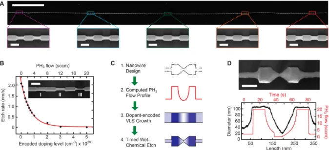
Figure 3.2: Characterization of NW growth, etching, and morphology. (A) Upper: SEM image of a grating-encoded NW more than 50 µm in axial length; scale bar, 5µm. Lower: Higher magnification SEM images of select sections of the NW in the upper panel; scale bars, 200 nm. (B) Radial etch rate of Si NWs as function of encoded P doping levels. Red curve represents the
For the synthesis of NWs with complex morphology, we measured the etch rate of Si NWs encoded with P doping levels ranging from 5.0×10²⁰to less than1.0×1019 dopants/cm3, as depicted in Figure 3.2B. Note that these doping levels were calculated from the gas-phase ratio of Si to P during CVD growth and the actual values could be lower as a result of incomplete P incorporation.131 Quantitative evaluation of the etch rate reveals a non-linear dependence on doping level that is well approximated with a single exponential function and varies from 2.1 nm/s for ‘intrinsic’ segments with doping levels <1.0×1019 cm−3 to negligible etching (<0.1 nm/s) with heavily doped segments. The exponential dependence is most likely a result of the logarithmic dependence of the Fermi level position on the doping level, which modulates the rate of Si oxidation and dissolution at the semiconductor-solution interface.132
The precise calibration of the NW growth and etch rates enables rational design and synthesis of arbitrary high-resolution morphologies, as outlined schematically in Figure 3.2C. This process involves 1) design of the morphological profile, 2) conversion of the physical profile into a dopant profile, 3) VLS growth of the dopant-encoded NW, and 4) wet-chemical etching. As an example, we used this procedure to form the bow-tie structure depicted in Figure 3.2D. The phosphine flow profile for the bow-tie (red curve Figure 3.2D) is complex, requiring over 25 changes in flow rate over a time scale of one minute. The diameter profile (black curve Figure 3.2D) shows the resulting structure to be smoothly tapered with a monotonically decreasing then increasing diameter that reduces to a diameter of∼15 nm at the narrowest point. Note that the phosphine flow profile was modified to be asymmetric around the flow minimum to account for dopants retained by the Au catalyst, a phenomenon termed the reservoir effect.65
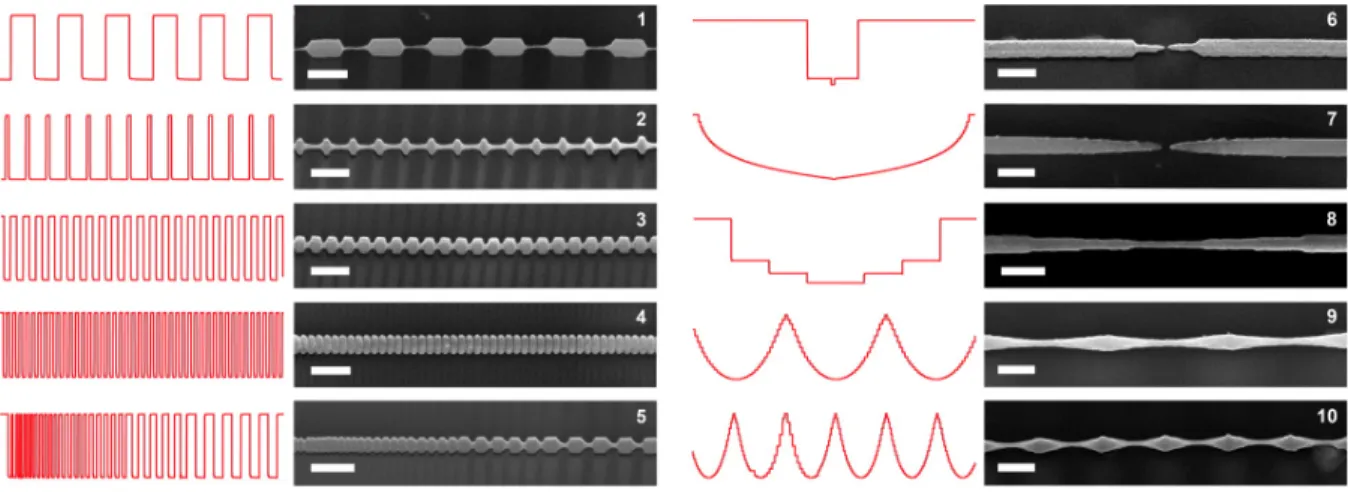
(image 8), and sinusoidal profiles (images 9–10). These morphologies could each enable a different class of NW-based technology. For instance, the suspended nanorods could be used as mechanical oscillators for nanoelectromechanical systems,135 periodic gratings for optical applications in
nanophotonics.136 and non-periodic gratings as a method to control thermal transport along the wires, enabling the use of Si as a thermoelectric material.137,138
Figure 3.3: SEM images and phosphine flow profiles for the synthesis of Si NWs with complex morphology. The measured phosphine flow profile used to encode the morphology of each segment is depicted in red to the left of each SEM image; all scale bars, 200 nm. The flow rates vary from 0 to 20 sccm for each NW.
interface due to electrostatic effects combined with the increased diffusion of dopants at elevated temperatures.137,139–141 Thus, thermal oxidation can also be a route to remove dopants from the NWs, decoupling the connection between doping level, Fermi level, and morphology.
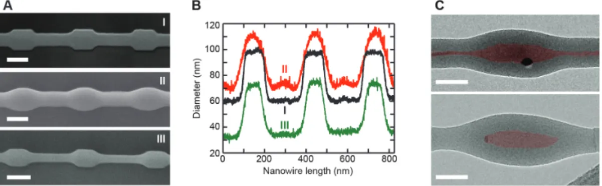
Figure 3.4: Thermal Oxidation of ENGRAVE structures. (A) SEM images of a single ENGRAVE NW before (top; I) and after (middle; II) thermal oxidation and after removal of the thermal oxide (bottom; III): scale bars, 100 nm. (B) Diameter profiles derived from the SEM images in panel A before (black; I) and after (red; II) thermal oxidation and after removal of the thermal oxide (green; III). (C) False-colored TEM images of etched NWs after thermal oxidation, in which the entire Si core (shaded red) retains its morphology (top) or the intrinsic segments are fully oxidized (bottom) leaving an ellipsoidal Si nanodot (shaded red): scale bars, 50 nm. Reprinted with permission from Christesen, J. D., Pinion, C. W., Hill, D. J., Kim, S. & Cahoon, J. F. Chemically Engraving Semiconductor Nanowires: Using Three-Dimensional Nanoscale Morphology to Encode Functionality from the Bottom Up. J. Phys. Chem. Lett. 2016, 7, 685–692. Copyright 2015 American Chemical Society.
3.4 Applications
preserved the high-resolution structures and nanogap morphology. We used finite-element optical simulations (see Figure 3.5C) to design Si/Au ENGRAVE structures with specific SPP characteristics. The NWs behave as plasmonic resonator antennas,144 in which the length of
the segments adjacent to the gap control the field enhancement as a result of constructive or destructive interference of the SPP wave along the NW axis.145,146 For a wavelength of 633 nm, we found that segments ∼775 nm in length were on-resonance, producing intense fields in the gap, while segments ∼1175 nm in length were off-resonance, exhibiting weaker field enhancement. As proof-of-concept, we performed SERS imaging on the Si/Au NWs coated with methylene blue.145,146We observed a greater than ten-fold Raman signal enhancement from the on-resonance structure, as shown by the spectra in Figure 3.5D. In addition, Raman imaging (see Figure 3.5E) confirmed that the signal enhancement is localized to a narrow spatial region around the gap. In comparison, the off-resonance NW shows a weak Raman signal arising from both the gap and the two ends of the rods, a result that is in good agreement with the optical simulations in Figure 3.5C. These results highlight the capability for ENGRAVE to serve as a simple route to create nanoplasmonic structures with tunable resonances for field-enhanced spectroscopy138 and nanophotonic technologies.143
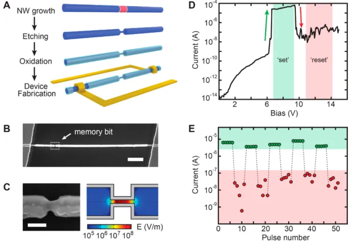
As a second application of ENGRAVE, we fabricated core/shell Si/SiO2 nanorod-encoded devices for use as resistive switches in non-volatile memory.117,147,148 The fabrication steps are illustrated in Figure 3.6A. First, an n-type/intrinsic/n-type NW was synthesized with a 50 nm intrinsic channel.2 Second, the channel was etched to a diameter of ∼30 nm to produce a
electric field within the narrow channel region, enabling a resistive switching effect as observed in a planar Si/SiO2 system.146,147 Initial current–voltage (I–V) measurements showed an Ohmic response from the device with a resistance of 54.7 kΩ, indicating the presence of a thin Si filament encapsulated by the SiO2shell. After an electroforming process consisting of multiple I–V sweeps at high bias (see Chapter 2.5 for details), the device converged to the characteristic "switching" I–V behavior (see Figure 3.6D) expected from a Si/SiO2 system.146,147The I–V curve exhibits a
low voltage region that "sets" the device to a low resistance state and a high voltage region that "resets" the device to a high resistance state. In the latter state, we observe variations in the current (see Figure 3.6D,E) similar to those reported previously in Si/SiO2 resistive switching memory devices and attributed to tunneling current fluctuations.147
To use the nanorod-encoded device as non-volatile memory, we applied sequential "set" and "reset" voltage pulses (100 s) of 8 V and 12 V, respectively, to reversibly change the resistance of the device. As shown in Figure 3.6E, we cycled the NW device through ten memory states and achieved on/off current ratios of nearly 102. With further development, we expect that at least 100 memory bits could be encoded on a single NW and lower voltage operation achieved with smaller nanorod segments. These initial results demonstrate the facile integration of ENGRAVE structures in electronic devices and furthermore highlight the emergent electronic characteristics that can be encoded through morphology.
3.5 Conclusion
In summary, we have demonstrated a method, termed ENGRAVE, to encode high-resolution morphology along the growth axis of Si NWs. We anticipate this process will be extended to other NW materials, such as GaAs/GaP94,150et al., that can be selectively etched with gas-phase
CHAPTER 4: ENCODING ABRUPT AND UNIFORM DOPANT PROFILES IN VAPOR–LIQUID–SOLID NANOWIRES BY SUPPRESSING THE
RESERVOIR EFFECT OF THE LIQUID CATALYST1
4.1 Introduction
Semiconductor NWs have been developed as a bottom-up technological platform for a va-riety of electronic,129,151 photonic,73,152,153 and photovoltaic119,154–156 devices. Several of these technologies require modulation of the NW composition along the growth axis to form heterostruc-tures that are required for specific device functions. For instance, NWs with n-type/intrinsic or p-type/intrinsic junctions have been explored as field-effect transistors, enabling both electronic devices125,129,157 and sensors.66,158,159 Similarly, NWs with p-type/n-type junctions have been synthesized in Si,69,85,133,149,159GaAs,69InP,160 etc, and used for photovoltaic devices,69,133,149 avalanche photodetectors,85 Esaki diodes,161,162 and light-emitting diodes.76,163 Nevertheless, it is generally believed that heterostructures formed by the VLS process will have broad junctions with a width approximately equal to the wire diameter.58,63,164 Considering the wide-ranging applications for NW heterostructures, it is increasingly important to understand the microscopic kinetic processes that govern heterostructure formation and to develop methods that overcome the limitations on the transition width.
During the VLS process (Figure 4.1A),165,166a liquid droplet composed of metal and semicon-ductor is formed by supplying a vapor-phase semiconsemicon-ductor precursor (e.g. SiH4 and GeH4) to a metal nanoparticle and raising the local temperature above the eutectic point for the two
materi-1
als. When the liquid droplet is supersaturated, which typically requires semiconductor weight fractions of 10-50%,64,167 a NW will nucleate and grow. Heterostructures are formed by altering the supply of vapor-phase precursors during VLS growth. However, the liquid droplet can act as a reservoir of material even after a precursor has been removed, causing the heterojunction to be broadened by a phenomena termed the “reservoir effect,” as illustrated in Figure 4.1B,C.65,67,96 This effect has been observed for heterostructures involving a change in dopants (e.g. P-doped Si52 and Si-doped GaAs57) and structures involving a change in semiconductor (e.g. Si/Ge58–60 and GaAs/InAs61,62) and has been described previously.
Figure 4.1: VLS NW growth and the reservoir effect. (A) Illustration of the key kinetic processes during Si NW growth: incorporation, evaporation, and crystallization. (B) Schematic of the reservoir effect, showing (left) a supply of P dopant precursor in the gas phase followed by (middle) removal of the gas-phase precursor with retention of P by the liquid catalyst and (right) subsequent depletion of P dopants from the liquid catalyst. (C) A plot of dopant concentration along the axial length of the NW.
mitigated by the simultaneous x-ray detection of four solid-state detectors in conjunction with the high-brightness Schottky-type field-emission gun of the STEM used in this work (FEI Tecnai Osiris; see Chapter 2.3.2). The transitions are also evaluated by wet-chemical etching of doped NWs using the recently reported ENGRAVE process.168 We develop a kinetic model of NW doping, which includes the microscopic processes of (1) P incorporation into the liquid catalyst, (2) P evaporation from the catalyst, and (3) P crystallization in the Si NW. We find a VLS growth regime in which the reservoir effect is fully suppressed because the rate of P evaporation greatly exceeds the rate of P crystallization. In this regime, NWs with diameters from 50 nm to 150 nm are encoded with abrupt and uniform dopant transitions, as verified by high-resolution morphologies encoded through the ENGRAVE process. The results suggest that the reservoir effect can be suppressed for any VLS growth system in which the rate of liquid-vapor equilibrium can greatly exceed the rate of NW growth.
4.2 Results
PH3 flow profile. Both measurements reflect dopant incorporation in the wire and are used to evaluate the abruptness of the n-type/intrinsic junctions.
Figure 4.3: Fit of the EDS spectrum. An example spectrum that was used to determine the relative concentration of Si and P to calculate the chemical doping level.
The resistivity measurements are in good agreement with previous reports on NW doping with PH3.130,131,169 However, a comparison of the chemical and active doping level measurements (right-hand axis of Figure 4.2C) indicates that less than 13% of the dopants in the NW are ionized and thus active for the highest doping levels, and less than 30% are active at the lowest doping level. Although donor deactivation has been reported in silicon nanostructures as a result of dielectric mismatch with the surrounding medium,170 the magnitude of the deactivation
determined here for NWs that are ∼100 nm in diameter is not well explained by this effect. Instead, the deactivation is likely due to lattice distortions and/or the formation of P dimers at the relatively low temperature (420◦C) used for VLS growth.171
Encoded Doping Level (cm−3) Resistivity (Ω/cm) Measured Doping Level (cm−3) 5.0×10²⁰ 1.75×10⁻² 1.69×10¹⁸
5.0×10²⁰ 1.21×10⁻³ 5.98×10¹⁹ 5.0×10²⁰ 2.50×10⁻³ 2.74×10¹⁹ 5.0×10²⁰ 1.72×10⁻³ 4.09×10¹⁹ 1.0×10²⁰ 4.29×10⁻³ 1.48×10¹⁹ 1.0×10²⁰ 3.09×10⁻³ 2.16×10¹⁹ 5.0×10¹⁹ 3.42×10⁻³ 1.93×10¹⁹ 5.0×10¹⁹ 7.27×10⁻³ 7.39×10¹⁸ 5.0×10¹⁹ 5.10×10⁻³ 1.19×10¹⁹ 5.0×10¹⁹ 1.06×10⁻² 4.12×10¹⁸ 2.5×10¹⁹ 8.86×10⁻³ 5.49×10¹⁸ 2.5×10¹⁹ 7.33×10⁻³ 7.30×10¹⁸ 2.5×10¹⁹ 5.45×10⁻³ 1.10×10¹⁹ 2.5×10¹⁹ 7.95×10⁻³ 6.48×10¹⁸ 2.5×10¹⁹ 9.47×10⁻³ 4.94×10¹⁸ 2.5×10¹⁹ 8.39×10⁻³ 5.98×10¹⁸
Table 4.1: Encoded doping levels and measured active doping levels. Measured resistivity values were converted into active doping levels using the resistivity of bulk Si as a function of P doping level.172
Figure 4.6: Arrhenius plot for VLS growth and VS overcoating. Logarithmic plot of the axial VLS NW growth rate (red circles and right-hand axis) and the radial VS overcoating rate (black squares and left-hand axis) as a function of inverse temperature. Dashed lines represent the best fit to the Arrhenius expression, yielding activation energies of 22±2 kcal/mol and 42 ±3 kcal/mol for VLS growth and VS overcoating, respectively. At a VLS growth temperature of 420 ◦C, the VS overcoating rate is less than 0.05 nm/min, but the VLS growth rate is still high because of the nearly two-fold difference in activation energy for the two processes. Error bars are comparable in size to the marker symbols and were omitted for clarity
High-resolution EDS and SEM imaging, as shown in Figure 4.7A and B, was used to quantify the abruptness of the n-type/intrinsic transitions. Line profiles generated from vertical sectioning of the images are displayed in Figure 4.7C. These profiles were fit to single-exponential functions convoluted with a Gaussian (equation 2.1) to extract the characteristic decay length, λ, of the transitions. The Gaussian convolution represents experimental broadening due to mass transport of etchant for SEM images and represents the finite beam size for EDS imaging (see Chapter 2.3.3 for details). The fits (dashed lines in Figure 4.7C) provide a reasonable representation of the transition widths, and the SEM data is also corrected (see Chapter 2.3.3) for the exponential relationship132,168 between the etch rate and encoded doping level. This analysis yields a measured transition length of 4 nm and 5 nm from the EDS and SEM data, respectively, in Figure 4.7C, demonstrating the good agreement between these two methods. The measured transition widths are substantially shorter than previous reports,58,164 and we develop below a kinetic model of NW doping in order to interpret the results. Note that for n-type/intrinsic/n-type sections, there is no apparent dependence of the transition width on intrinsic segment length. Diameter profiles and SEM images in Figure 4.7D and 3E show the same profile for intrinsic segments 10 nm to 200 nm in length; however, the smaller segments are etched to a lesser extent presumably because mass transport to the etched region is hindered by the small dimensions. In addition, the first transition region (n-type/intrinsic) shows the same abruptness (<10 nm) as the second transition (intrinsic/n-type).
4.3 Kinetic Modeling and Analysis
We analyze P dopant incorporation in Si NWs using the three microscopic kinetic processes depicted in Figure 4.9A: P incorporation, P evaporation, and P crystallization.173 By analyzing
CVD system, such as switching speed of the mass flow controllers and rate of gas exchange in the system, has no influence on the observed transition width, which is verified by control growth studies (see Figure 4.8). Second, we assume the NW growth rate is independent of the concentration of vapor-phase PH3 or P dissolved in the liquid, which is supported by our previous studies of VLS growth kinetics.166 Third, we assume that prior to a transition, the dopant has reached a steady-state concentration and is uniformly distributed in the liquid catalyst, which is confirmed by the homogeneity of the P signal in Figure 4.2. Note that the kinetic analysis below is used to interpret the transition width of n-type/intrinsic transitions but not intrinsic/n-type transitions. For the latter transitions, in which the n-type region is grown after the intrinsic region, an abrupt, sub-10 nm transition is consistently observed. We attribute this abruptness to a uniformly high rate of P incorporation under all VLS growth conditions.
Figure 4.8: Transition width at various carrier gas flow rates with a constant NW growth rate. The H2 carrier gas flow rate was altered while maintaining a constant total reactor pressure of 40 Torr. The flow rate of SiH4 was adjusted to maintain the same partial pressure of SiH4 and thus the same NW growth rate under all conditions.
Nd=
kP CCP(l)πr2ΩP
kSiCCSi(l)πr2ΩSi
≈ kP CCP(l) kSiCCSi(l)
(4.1)
wherekP C is the rate constant for P crystallization (units of nm/s), kSiC is the rate constant for
Si crystallization (units of nm/s), CP(l) is the concentration of P in the liquid catalyst, CSi(l) is the concentration of Si in the liquid catalyst, r is the radius of the solid NW, and ΩSi and
ΩP are the Si and P volumes per atom, respectively. We also assumeΩSi∼ΩP, leading to the
simplification shown on the right-hand side of equation 4.1. During an n-type/intrinsic transition, the dopant width is dictated by the time-dependence of CP(l), which decreases as a result of P crystallization and evaporation as:
dCP(l)
dt =−kP ECP(l) S
V −kP CCP(l) A
V (4.2)
wherekP E is the rate constant for P evaporation (units of nm/s),S is the liquid-vapor interfacial
surface area, V is the volume of the liquid catalyst, and A is the cross-sectional area of the NW (equal to r2). Solving equation 4.2 forCP(l) and inserting the result into equation 4.1 assuming
a partial sphere geometry for the liquid catalyst yields:
Nd(t) =
kP CCo,P(l) kSiCCSi(l)
exp
−32RkP E + r
2
R+αkP C
(R+α)(2R−α) t
(4.3)
where Co,P(l) is the initial concentration of P in the metal catalyst, R is the liquid catalyst diameter,αis√R2−r2, andtis the total amount of time after the P precursor has been turned off. The growth rate,G, of the NW, as developed previously, is:
G= L