5376
THE DESIGN OF HIGH PERFORMANCE
THREE INPUT XOR GATE BASED ON
COMPOUND GATE METHODOLOGY
Chaitanya kommu, Dr. A Daisy Rani
Abstract— The low power and high speed fundamental building blocks are essential to construct arithmetic circuits. Three input Exclusive-OR(XOR) is presented here based on compound gate method. The high performance is achieved by reducing input capacitance, choosing suitable input to propagate and avoiding glitch. The proposed XOR gate requires less number of transistors (i.e. only 8 transistors) and offers 60.62% of power dissipation reduction and 13.71% less propagation delay compared to two level conventional static XOR gate. The simulation is performed based on 32nm technology node(PTM-models) using Hspice Synopsis simulation tool.
Index Terms— Arithmetic circuits, Modulo XOR gate, Low Power CMOS, Pass transistors, Transmission gate, compound gate, Scaling.
—————————— ——————————
1 INTRODUCTION
Now a day’s the continuous growth of scaling of integration leads to the requirements of low power, high performance arithmetic circuits, which are predominantly used in portable devices and today’s advanced VLSI chip design [1], [2], especially applications like Artificial Intelligence and Internet of Things (IoT). The performance parameters which are influencing the low power dissipation is govern by the fundamental power equation as shown in following.Now a day’s the continuous growth of scaling of integration leads to the requirements of low power, high performance arithmetic circuits, which are predominantly used in portable devices and today’s advanced VLSI chip design [1], [2], especially applications like Artificial Intelligence and Internet of Things (IoT). The performance parameters which are influencing the low power dissipation is govern by the fundamental power equation as shown in following.Various parameters are influence the dynamic power which are power supply(Vdd), frequency of input signal, internode capacitances, activity of switching and Short circuit current. Therefore, these parameters are responsible for reduced power dissipation. It is evident that primarily the low power circuit depends on how one can implement the circuit which is also called as the type of logic style. Let us see the influence of logic style on low power requirements. The downsizing of transistor reduces the internal node switching capacitance which is possible by choosing the best possible logic style. Moreover, functionality of the circuit should not be degrading because of voltage scaling. Therefore, it is noticed that the chosen logic style must be robust for downsizing of transistors and supply voltage scaling. The supply voltage and the logic style are related indirectly in terms of critical signal paths. The type of realization of a logic function influence the switching
activity of the circuits. It is observed that the dynamic realization has more activity than static realizations [2], [3]. The input signal slopes and transistor sizing are strongly effects the short circuit current. The reduction in short circuit current is possible by giving steep and balanced input signal slopes. A good logic style allows decoupling of input and outputs of the logic gates, good driving capability and full signal swings so that it is easy to use and work reliably. Thereby for cell based designs functionality and synthesis of logics are mostly depending on these properties [3]- [4].Rest of the paper is organized as follows: Session-2 discuss about overview of logic styles necessary for design, the design of three input XOR is explained in Session-3 and Session-4 mention the simulation setup and result discussion, finally in Session-5 conclude the paper.
2
OVERVIEW
OF
LOGIC
STYLES
2.1 Static CMOS
The Static CMOS logic implementation of digital integrated arithmetic circuits offers low static power and best choice for power efficiency, it also observes the high propagation delay compared it its counterparts [5]. The construction with pull-up and pull-down networks of static realization actually leads to low power constraints. The pull-up network drags the output to logic high value whereas pull-down network pulls down the output node to logic low level. The general construction of static CMOS is shown in Fig.1.1(a). In general, pMOS FETs for Pull-up network and nMOS FETs for pull-down network are used. For example, the static CMOS NAND and NOR gate are shown in Fig.1.1(b) and Fig.1.1(c) respectively. This implementation promises the very low static power since at a time only one network is active to obtain the output signal and good noise margin but requires more number of transistors if the fan in of the digital circuit increases. It is possible to reduce the number of transistors by taking two level realization of large fan in circuits. It is noticed that the input capacitance and propagation delay of the circuit will increases.
————————————————
Chaitanya kommu is currently pursuing Ph.D. program in Instrument Technology, in Andhra University, Visakhapatnam, India, PH-9951997305. E-mail: [email protected]
5377 Fig.1.1 (a) General structure of a CMOS gate. (b) CMOS
NAND. (c) CMOS NOR.
2.2 Pass Transistor Logic(PTL)
Another way to realize the logic circuits by using Pass Transistor Logic(PTL) as shown in Fig.1.2. The one input is applied at ‘A’ and other input is at ‘B’, signal ‘Y’ is taken as output. It is more attractive to circuit realization in terms of utilization of less number transistors [6]- [10]. It is observing that inputs are not only applied at gate terminal of MOSFET but also at the source/drain terminals of transistors therefore it is also called as gate no-restored logic implementation. there is a serious problem inherent to the pass gate logic is that it suffers from threshold problem. For example, let us consider nMOS transistor and apply logic high at gate terminal as well as source/drain terminal it is observe that only (VDD-Vth) is the output signal strength after that the nMOS enter into cutoff region.
Similarly, the maximum output voltage of pMOS transistor is Vtp. Hence pMOS is good for logic high Signal passage but bad for logic low signal whereas nMOS is good for logic low and bad for logic high. Therefore, the maximum output voltage for pass gate realization suffers from signal strength. This problem is solved by different methods.
Fig.1.2 Pass Transistor
2.3 Transmission Gate Technology(TGL)
The threshold problem of pass gate implementation can be eliminated by the Transmission Gate Technology(TGT). The circuit diagram and circuit symbol is shown in Fig.1.3(a) &(b) respectively. It is observed that the parallel connection of nMOS and pMOS transistors gives the best possible combination to encounter the swing loss problem [11]- [12]. The electrical properties of TGT is shown in Fig.1.3(c). If the input is Logic High, then pMOS will give a chance for the input signal pass through it because it offers less resistive path for logic high whereas for the signal of logic low will choose the nMOS transistor path where it finds the low resistive path for active low signals.
Fig.1.3 (a)TG Circuit (b)Circuit Symbol (c)Resistance characteristics of TG
Therefore, the threshold problem is easily eliminated by the TGT method. The transistors count increase but not more than that of conventional Static CMOS logic implementation.
3
DESIGN
OF
THREE
INPUT
EXCLUSIVE-OR
GATE
The exclusive OR gate is a fundamental building primitive for adders which are mostly used in almost all the arithmetic circuits [6]. The efficient realization of high Fan-in XOR gate defines the performance of digital circuits like adders, magnitude comparators etc. in this section we discuss about the design of three input gate. The block diagram and functional table is shown in Fig.2.1(a), (b). The conventional approach to implement three input static XOR gate is by using 2 two input XOR gates, that means it uses two level circuit as shown in the Fig.2.2(a). the realization of the two input XOR gate is shown in Fig.2.2(b). It observes from the Figure that the propagation delay of the three input XOR gate using two level method will increase as well as this implementation prone to glitch problem. Therefore, with the help of Pass gate and Transmission gate methodology it is possible construct three input XOR in a compound gate technique. The basic design constrains to achieve low power and high speed is that, avoid the two level realization, eliminating the inverting inputs to pass through source/drain terminals of pass transistors and attain the good logic swing (i.e. reduce the threshold loss problem)
Fig.2.2 (a) Block diagram (b) Functional Table (c) Two level Three input XOR gate
The logical expression that governs the functional table is as shown follows
---(2)
Where m=minterms, these are observed for the input combinations 1,2,4,7.
Equation (2) can be written as
---(3)
---(4)
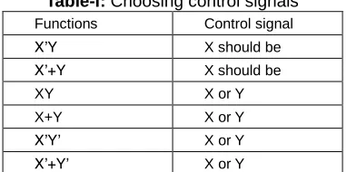
5378 Table-I: Choosing control signals
Functions Control signal
X’Y X should be
X’+Y X should be
XY X or Y
X+Y X or Y
X’Y’ X or Y
X’+Y’ X or Y
For example, From the table if any function having the possibility shown. we choose complemented signal as control signal whereas Un-complemented signal as propagate signal. Therefore, Equation (4) contains the input signal “A” as control signal which means this signal is applied at the gate terminal of the MOS transistor. Moreover, input “A” can be treated as Un-complemented input for pMOS transistors as well, shown in Fig.2.3. similarly, the signal “B” also treated as control signal for nMOS and “B’” pMOS transistor’s control signal. The input signal “C” considered to be propagate signal since this input signal transitions are more compared to other input signals (B, C). Therefore, we will measure the accurate results related to critical path delay and power dissipation.
Fig 2.3 Proposed three input XOR gate
As shown in Fig.2.3, the upper transmission gate is used to attain the full swing if at all the upper pass transistors produces threshold deviation which is occurred when ABC combination as “010”, “100” preferably. For all other combinations placing output buffers to get good logic value in the view of less number of transistors to utilize. Therefore, the proposed XOR gate avoid glitch problem effectively without using two-level circuit like static CMOS gates.
4
SIMULATION
RESULTS
AND
DISCUSSION
Simulations are performed using H-Spice Synopsis tools. Simulations are done at 0.8v, 0.9v, 1.0v and 1.1v supplies and under 32nm technology PTM model file for MOS transistors [13]. Power consumption and time delay are calculated using features provided in the H-Spice Software. PDP is calculated as the product of Average Power consumption and propagation time delay. All circuits are simulated with varying frequency of 0.5GHz, 1GHz, 2GHz, and 3GHz at a temperature of 25o C and the average power/delay is calculated and presented in each case. The Ln=Lp=32n, and Wn=48n and Wp=64n for fare estimation of proposed gate sizing. The two level design of static gate prone to glitch problem so to avoid this we used hazard filtering technique where without effect the critical path signal delays, output size logics are modified at their aspect rations. The W/L rations of static gate at the output size is increased by 2 times than that of proposed gate. Therefore, the buffer gates are having Wnp
(width of proposed nMOS) =32n and Wpp (width of proposed pMOS) = 64n, similarly Wn= 128n Wp=128n for static gates.
4.1 Simulation waveform
The simulation wave form is shown in Fig.3.1 for all possible input combinations.
4.2 Results discussion
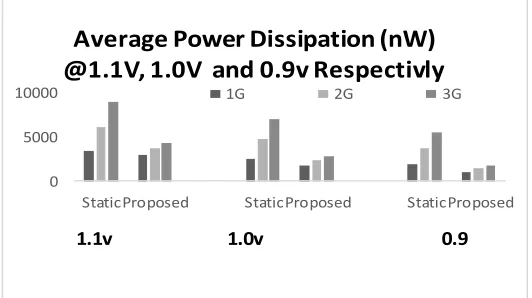
The proposed XOR gate compared with standard two level static CMOS XOR gate. From the Table-II the proposed XOR gate is best in terms of low power consumption foe all supply voltages and at all input frequency variations. It is noticed that at input signal frequency of 1GHz for supply voltages of 1.1v, 1.0v and 0.9v, the percentage reduction of average power consumption is 10.60%, 27.53% and 44.82% respectively. At the input signal frequency of 2GHz for 1.1v, 1.0v and 0.9v, the percentage reduction of average power consumption is 39.58%, 50.79% and 61.85%, respectively. Similarly input signal frequency of 3GHz at the supply voltages of 1.1v, 1.0v and 0.9v, the percentage reduction of average power consumption is 52.20%, 60.60% and 69.06% respectively. Therefore, from the percentage values it is observed that by scaling down the supply voltage from 1.1v to 0.9v at the input signal frequencies of 1GHz, 2GHz and 3GHz, the average percentage of power dissipation of proposed XOR is 27.65%, 50.74% and 60.62% compared to static gate respectively.The propagation delay of static and proposed gate is shown in Table-III. At the supply voltage of 1.1v and for the frequency of input signal 1G, 2G, 3G, percentage of propagation delay reduction is 26.85%, 26.77% and 26.63% respectively. Similarly, at the power supply of 1.0 volts for the frequency of input signal 1G, 2G, 3G, Delay reduction is about 13.96%, 13.97% and 13.71%. But at the supply value of 0.9v delay is increased on an average by 18.5%
5379 Table-II: Simulation results of Average Power Dissipation
Static XOR gate Input signal
Frequency
Average Power Dissipation(nW)
1.1v 1.0v 0.9v
1G 3362.5 2511.6 1909.8
2G 6133.6 4750.7 3679.2
3G 8978.9 7042.7 5490.1
Proposed XOR gate Input signal
Frequency
Average Power Dissipation(nW)
1.1v 1.0v 0.9v
1G 3005.8 1820.1 1053.8
2G 3705.8 2337.5 1403.4
3G 4291.5 2774.6 1698.4
Table-III: Simulation results of Propagation Delay
Static XOR gate Input signal Frequency
Propagation Delay(pS)
1.1v 1.0v 0.9v
1G 69.1317 82.1852 99.7299
2G 69.0919 82.1785 99.6296
3G 69.0327 82.1673 99.5372
Proposed XOR gate Input signal Frequency
Propagation Delay(pS)
1.1v 1.0v 0.9v
1G 50.5648 70.7064 118.0513
2G 50.593 70.6909 118.1689
3G 50.6451 70.8997 118.5569
Table-IV Power Delay Product (PDP)
Static XOR gate PDP( aW-S)
1.1v 1.0v 0.9v
1G 232.45 206.41 190.46
2G 423.78 390.41 366.55
3G 619.83 578.67 546.46
Proposed XOR gate
PDP( aW-S)
1.1v 1.0v 0.9v
1G 151.98 128.69 124.4
2G 187.48 165.23 165.83
3G 217.34 196.71 201.35
4.3 Graphical Representation of comparisons
The graphical representation of comparisons is shown in the Fig.3.2 to Fig. 3.4
Fig. 3.2 Comparison of Average Power Dissipation at supply voltages 1.1v, 1.0v and 0.9v
Fig. 3.3 Comparison of Propagation Delay at supply voltages 1.1v, 1.0v and 0.9v
Fig. 3.4 Comparison of PDP at supply voltages 1.1v, 1.0v and 0.9v
Therefore, it is evident that the PDP valve of this XOR is better compared to static gate in spite of some delay concern related to 0.9v and for all frequencies. For low power and high speed designs compound gate based XOR is suitable but gate restoration circuits are used at the output of the XOR. Hence the proposed XOR works better in terms of power dissipation and reasonable operating speed.
5
CONCLUSION
This paper has introduced an efficient implementation of three input XOR gate using non restored logic and transmission gates. The two level static gate is compared with compound gate and found that the proposed XOR gate is best in terms of power dissipation and reasonable frequency of operation. This is achieved by using less number of transistors, eliminating the glitch problem (generally occurs in two level circuits) and avoiding the complement inputs to propagate. The proposed and static three input XOR gates were simulated at different voltages and at different frequencies. It observed that the proposed standard cell consumed 60.62% less power and 0
5000 10000
StaticProposed StaticProposed StaticProposed
1.1v 1.0v 0.9
Average Power Dissipation (nW)
@1.1V, 1.0V and 0.9v Respectivly
5380 13.71% decreased propagation delay compared to
conventional static two level CMOS logic style at 0.9v supply voltage. Therefore, the proposed three input combinational gate is used in complex digital designs especially where area reduction is essential. Moreover, the presented high performance characteristics can benefit in the applications of ASIC design.
REFERENCES
[1] N. H. E. Weste and D. M. Harris, CMOS VLSI Design, Circuits and Systems Perspective, 4th ed. Boston, MA, USA: Addison- Wesley, 2011.
[2] Chandrakasan Anantha P., Nikolić Borivoje and Rabaey Jan M (2003). Digital integrated circuits: a p (2ndedition). Pearson Education
[3] R. Zimmermann and W. Fichtner, “Low-power logic styles: CMOS versus pass-transistor logic,” IEEE J. Solid State Circuits, vol. 32, no. 7, pp. 1079–1090, Jul. 1997.
[4] K Chaitanya and A. Daisy rani, “The Mixed Logic Style based Low Power and High Speed 3-2 Compressor for ASIC designs at 32nm Technology” (IJEAT) ISSN: 2249 – 8958, Volume-9 Issue-1, October 2019”.
[5] Design of Low-Power High-Performance 2–4 and 4– 16 Mixed-Logic Line Decoders Dimitrios Balobas and Nikos Konofaos, “IEEE Transition on circuits and system—II: Express Briefs, VOL. 64, NO. 2, FEBRUARY 2017.
[6] M. Chaitanya, Chaitanya Kommu, “Modified Low-Power Hybrid 1-Bit Full Adder”, Proceedings of 2nd International Conference on Micro-Electronics, Electromagnetics and Telecommunications, © Springer Nature Singapore Pte Ltd. 2018
[7] Deepa Sinha, Tripti Sharma, G. Sharma, Prof.B.P. Singh, “Design and Analysis of low Power 1-bit Full Adder Cell”, IEEE, 2011.
[8] K. Yano et al., “A 3.8-ns CMOS 16 × 16-b multiplier using complementary pass-transistor logic,” IEEE J. Solid -State Circuits, vol. 25, no. 2, pp. 388–393, Apr. 1990.
[9] V. G. Oklobdzija and B. Duchene, “Pass-transistor dual value logic for low-power CMOS,” in Proc. Int. VLSI Technol.,1995, pp. 341–344.
[10] D. Markovi´c, B. Nikoli´c, and V. G. Oklobdžija, “A general method in synthesis of pass-transistor circuits,” Microelectron. J., vol. 31, pp. 991–998, 2000.
[11] X. Wu, “Theory of transmission switches and its application to design of CMOS digital circuits,” Int. J. Circuit Theory Appl., vol. 20, no. 4, pp. 349–356, 1992.
[12] Maytham Shams and Mohamed Elmasry “Estimation and Optimization of Delay in Popular CMOS Logic Styles”, The13th International conference onMicroelectronics-2001.