T he D ev elo p m en t
o f
T he M IC D etecto r
for
Space A p p lication s
A Thesis Subm itted for the Degree
of
D octor of Philosophy of the University of London
b y
Jonathan Gareth Beilis
A
UCL
D e p a rtm e n t of P hysics Sz A stro n o m y
U n iversity College L ondon
U niversity of L ondon
ProQuest Number: 10044263
All rights reserved
INFORMATION TO ALL USERS
The quality of this reproduction is dependent upon the quality of the copy submitted.
In the unlikely event that the author did not send a complete manuscript and there are missing pages, these will be noted. Also, if material had to be removed,
a note will indicate the deletion.
uest.
ProQuest 10044263
Published by ProQuest LLC(2016). Copyright of the Dissertation is held by the Author.
All rights reserved.
This work is protected against unauthorized copying under Title 17, United States Code. Microform Edition © ProQuest LLC.
ProQuest LLC
789 East Eisenhower Parkway P.O. Box 1346
A b stra ct
Since the development of the original Boksenberg IPCS a t UCL several innovations have
led to a highly compact, lightweight detector, the MIC-IPCS. A version specially designed
for space applications is described here. The design has been based around the special
requirem ents of a space based system.
The design and operation of each component of the detector is described. The detector
incorporates a microchannel plate intensifier specifically designed for photon counting.
The properties of the intensifier th a t lim it the detector performance are considered. The
o u tp u t of the intensifier is coupled to a CCD via a fibre optic taper. The characteristics
of fibre coupling are discussed and the effects the fibre tap er introduces via pin cushion
distortion are considered in detail. A fast scanning CCD is used as a readout device and
the operation and design of the camera is described. The CCD d a ta is presented to the
im age processing electronics th a t perform various im po rtan t functions on the d ata. The
design of each component circuit is considered in detail, in particular, a new interpolative
centroiding technique has been developed.
Tests were carried out to assess the performance of the detector. The results are
discussed and the performance characteristics of the detector evaluated.
I have been personally responsible for the design and testing of the processing elec
tronics, the analysis of the phosphor decay characteristics of the image intensifier and for
analysis of fibre taper distortion and efficiency. Additionally, when construction of the
detector was complete, I took p art in all the subsequent system tests and d a ta reduction
A ck n ow led g em en ts
I would like to thank my supervisor, John Fordham , for all his help and advice over the
past three years and for generally sorting things out. I would also like to thank Dave Bone
for knowing all the answers; Tim N orton for all his inform ation and Dave Rooks for his
speedy photographic work.
On the non-academic side I would like to thank my parents for their support. Moldy
deserves thanks for being a good laugh and for keeping me sane. Finally, I m ust thank
the other people who have kept me amused or relieved the boredom - Helen, Helen M.,
C o n ten ts
T itle P a g e 1
A b str a c t 2
A ck n o w led g e m en ts 3
1 In tr o d u ctio n 13
1.1 Present Day Electronic Detectors for A s t r o n o m y ... 15
1.1.1 The C C D ... 15
1.1.2 Photon Counting D e te c to r s ... 16
1.2 The History of the Development of M I C ... 19
1.2.1 The I P C S ... 19
1.2.2 The C C D -IP C S ...21
1.2.3 The MicroChannel P late Intensified CCD Image Photon Counting D etector ( M I C - I P C S ) ...24
2 T h e Space B a sed M IC 26 2.1 The Application of a Space Based S y s te m ... 27
2.2 Scientific Requirements of the XMM Optical M o n ito r...28
2.2.1 Overview of the X M M -M IC ... 30
3 T h e Im age In te n sifier 34 3.1 In tro d u c tio n ... 34
3.2 The Design and O peration of the In te n s ifie r... 37
3.2.3 The Channel P l a t e s ...42
3.2.4 The Phosphor Screen... 46
3.2.5 Intensifier H o u s in g ... 48
3.2.6 The Intensifier Power S u p p l y ... 48
3.3 Lim itations on the Performance of the I n te n s ifie r...49
3.3.1 R esolution... 49
3.3.2 Detective Q uantum E fficiency...51
3.3.3 L ife tim e ... 52
3.3.4 Dynamic R a n g e ...57
3.3.5 O ther Intensifier Properties Afifecting D etector P erfo rm a n c e ... 67
4 F ib re O p tics 70 4.1 In tro d u c tio n ... 70
4.2 The Fibre Optic O utput of the I n te n s if ie r ... 71
4.3 The Fibre Optic T a p e r ...72
4.3.1 A Comparison of Lens and Fibre Optic C o u p lin g ...74
4.3.2 Analysis of Pin-cushion D istortion for the Correction of Guide Star Positions ...77
4.4 The Fibre Optic Block on the C C D ...92
4.5 The Effect of Radiation on Fibre Optic G l a s s ...93
5 T h e C C D C am era 96 5.1 In tro d u c tio n ...96
5.1.1 The O peration of C C D s ... 97
5.2 CCD P e r f o r m a n c e ... 101
5.3 The CCD C a m e r a ...102
5.3.1 The Signal Processing and Digitizing S e c t i o n ... 103
5.3.2 The CCD Support S ectio n ...108
5.4 The Effect of Radiation on the C C D ... 112
5.4.1 A Summary of Radiation E f f e c t s ...112
5.4.2 Radiation Effects for the MIC CCD ... 114
6 T h e Im a g e P ro c e ssin g E lectro n ics 117
6.1 In tro d u c tio n ... 117
6.2 The Command I n te r f a c e ...122
6.2.1 Circuit D escrip tio n ... 122
6.3 D ata Analysis A r r a y ... 126
6.3.1 Circuit D escrip tio n ...128
6.4 Event V a l i d a t e ...135
6.4.1 C riteria for event determ ination ...135
6.4.2 Circuit D escrip tio n ... 137
6.5 Multiple Event D iscrim in ate...140
6.5.1 Introduction ... 140
6.5.2 Principle of O peration of the Multiple Event D is c r im in a to r ... 141
6.5.3 Circuit D escrip tio n ... 144
6.6 C e n tro id ... 146
6.6.1 Introduction ...146
6.6.2 The Problem of P a tte rn Noise and its R e m o v a l...148
6.6.3 The Centroiding Technique Used with M I C ... 151
6.7 Address G e n e r a to r ... 167
6.7.1 Circuit D escrip tio n ... 169
6.8 The Frame S t o r e ...177
6.8.1 Circuit D escrip tio n ... 178
6.9 The Memory I n te r f a c e ... 181
6.9.1 Introduction ...181
6.9.2 The Read-Modify-Write Cycle ... 182
6.9.3 O peration of the Memory Interface as a S la v e ... 194
7 S y s te m P erfo rm a n ce 197 7.1 In tro d u c tio n ... 197
7.2 Photocathode Sensitivity ... 201
7.3 Dynamic R a n g e ...202
7.3.1 The lower l i m i t ... 203
7.3.2 The Bright L i m i t ...203
7.5 System Detective Q uantum E ff ic ie n c y ...218
7.6 D etector U n if o r m ity ... 218
7.6.1 Fixed P attern N o i s e ...220
7.6.2 The Effi^ct of Fibre Optic Multifibre Junction D e f e c t s ... 222
7.6.3 The Effect of low quantum efficiency CCD p i x e l s ... 223
7.6.4 O ther D etector N on-U niform ities...223
7.6.5 Variation of P attern Noise with Count R a t e ...224
7.7 Observing T r i a l s ... 226
7.7.1 The Observing P r o g r a m m e ... 226
7.7.2 O b se rv in g ...227
7.7.3 D ata A n aly sis... 230
8 C o n clu sio n s 235 8.1 S u m m a r y ... 235
8.2 Future D evelopm ents...238
R eferen ces 243
List o f T ables
2.1 Prim ary scientific requirements of the photon counting detector for XMM , 29
2.2 Required characteristics of the XMM -M IC ... 29
4.1 Coefficients of a straight line fit to fibre taper grid l i n e s ...81
4.2 Errors introduced by the fibre taper in a 300^m straight l i n e ... 85
4.3 Deviations from the d ata of the polynomial fits to pin cushion distortion . . 86
4.4 Coefficients of a 3rd order polynomial fit to horizontal errors introduced by
pin cushion d i s t o r t i o n ...87
6.1 Commands used to communicate w ith the image processing c h a s s is ...123
6.2 Boundary positions and centroid positions for equzd c h a n n e l s ... 153
6.3 Boundary positions and counts per channel for four iteratively corrected
flat fields ...161
6.4 Sequencer states for the memory in te r f a c e ...188
List o f F igures
1.1 Block diagram of the original I P C S ... 19
1.2 Cross section through the EMI four stage image in ten sifier...22
1.3 Block diagram of the C C D - I P C S ... 23
2.1 The XMM sp a c e c ra ft...28
2.2 An example of the use of the windowing f a c ility ...30
2.3 Block diagram of the X M M -M IC ...31
2.4 The prototype MIC s y s t e m ... 32
3.1 Schematic of the various stages of the MCP in te n s if ie r ...34
3.2 The 25mm microchannel plate image in te n s ifie r...37
3.3 Schematic of a cross section of the intensifier incorporated into the detector h e a d ... 38
3.4 Transmission of MgFg and Sapphire w in d o w s ...39
3.5 Hexagonal close packed structure of the MCP pores ...43
3.6 Cross section through a typical m ic r o c h a n n e l...44
3.7 Typical MCP intensifier pulse height d is tr ib u tio n ... 46
3.8 Typical EMI intensifier pulse height distribution ... 47
3.9 Measured phosphor decay c u r v e ...58
3.10 Relationship between times required to evaluate the phosphor decay . . . . 60
3.11 Fit to the phosphor d e c a y ... 62
3.12 Energy em itted by the phosphor as a function of t i m e ... 63
3.13 Ratio of the height of the residual to the height of the real e v e n t ...64
4.3 Propagation of light down a tapered f i b r e ... 74
4.4 Spot diagram for the CCD-IPCS relay lens ... 75
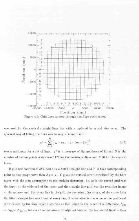
4.5 Grid lines as seen through the fibre optic ta p er... 79
4.6 Exaggeration of the distortion introduced on a grid by the fibre taper . . . 80
4.7 Errors of a fibre optic image grid from a straight line g r i d ...82
4.7 ( c o n t d . )... 83
4.7 ( c o n t d . )... 84
4.8 Greyscale plot of the horizontal pin cushion d i s t o r t i o n ... 88
4.9 Greyscale plot of the vertical pin cushion d is to rtio n ...89
4.10 Absolute error introduced by pin cushion d isto rtio n ...90
5.1 Generalised structure of a charge storage site of a buried channel CCD . . . 97
5.2 Clocking voltages and potential well structures th a t give rise to charge transfer 98 5.3 The frame transfer C C D ... 99
5.4 The cam era electro n ics...104
5.5 Block diagram of the CCD camera e le c tro n ic s...105
5.6 Block diagram of the video processor section of the CCD camera electronics 105 5.7 Timing for the signal processing and digitizing section of the CCD cam era . 106 5.8 The Flash Analog-to-Digital C o n v e rte r... 107
5.9 A simple example of CCD windowing ... 110
6.1 Block diagram of the image processing electro nics... 118
6.2 The image processing c h a s s i s ...121
6.3 The command i n t e r f a c e ... 124
6.4 Typical timing for the write cycle of the command in te r f a c e ... 125
6.5 The way in which a photon event might appear on the C C D ... 126
6.6 Schematic showing the idea behind the operation of the D ata Analysis A rray 127 6.7 D ata analysis array root d ia g r a m ... 129
6.8 The array of the d ata analysis a r r a y ... 130
6.9 D ata analysis timing c irc u itr y ...131
6.10 Timing of the various components of the d ata analysis a r r a y ... 133
6.11 Cross hair used by Event Validate and a possible profile of the d ata . . . . 135
6.13 Root diagram of event validate and c e n tro id ... 138
6.14 The event validate c i r c u i t ... 139
6.15 Dynamic range curve illustrating the non-linearity seen a t higher count rates 141 6.16 Two events not exactly coincident ... ... . 142
6.17 Possible pulse energy for single and double e v e n ts ...143
6.18 The pulse energy discriminator c i r c u i t ...145
6.19 A pixelated event p ro file ...147
6.20 P a tte rn noise introduced into a flat field as a result of centroiding errors . . 148
6.21 Profile of a real event seen w ith M I C ...149
6.22 Asym metry of photon e v e n t s ...150
6.23 An illustration of how the size of memory needed for a look-up table is greatly reduced by partially calculating the centroid in h a r d w a r e ... 153
6.24 Flow diagram depicting the procedure for correcting the p attern noise . . . 155
6.25 Centroid look-up tables c i r c u i t r y ... 156
6.26 Circuitry for calculating M and N of the centroiding a l g o r i t h m ... 157
6.27 Four flat fields showing the gradual removal of the fixed p attern noise with each successive i t e r a t i o n ... 160
6.28 Fourier transform power spectra of corrected and uncorrected flat fields . . 162
6.29 Eight spectra associated with the same pixel ...164
6.30 Ideal form in which to have a memory address ... 168
6.31 Memory allocation w ith a window length of 256 ... 168
6.32 W aste of memory encountered when the window length is not 256 168 6.33 Block diagram of the address generator ... 170
6.34 Root diagram of the address g e n e r a to r ... 171
6.35 Address generator c i r c u i t r y ... 172
6.36 Control circuitry for the transfer of d ata to the m e m o r y ...173
6.37 FIFO write cycle t i m i n g ...175
6.38 FIFO read cycle timing ...176
6.39 The frame store c ir c u it...179
6.40 Schematic of the memory interface in m aster m o d e ...183
6.41 Root diagram of the memory in te r f a c e ...187
6.43 Address handling section of the memory in te rfa c e ... 190
6.44 D ata handling section of the memory i n t e r f a c e ... 191
6.45 Timing diagram for read -m o d ify -w rite...192
6.46 The tim er of the memory i n t e r f a c e ... 196
7.1 Signal induced background seen w ith ITL image in te n s if ie r s ... 199
7.2 RQE of ITL p h o to c a th o d e ... 201
7.3 RQE of DEP p h o to c a th o d e ... 202
7.4 F lat field dynamic range curve on full f o r m a t ... 204
7.5 Point source dynamic range curve on full form at ... 204
7.6 Theoretical point source dynamic range curves for two frame r a t e s ...206
7.7 Point source dynamic range curve on a format of 256x2048 ... 207
7.8 F lat field dynamic range curves for three multiple counting thresholds on a form at of 2048x2048 ... 208
7.9 Point source dynamic range curve for three m ultiple counting thresholds on a form at of 2048x2048 ... 209
7.10 Point source dynamic range curve for three m ultiple counting thresholds on a form at of 2048x2048 ... 210
7.11 Real and simulated dynamic range curves showing the effect of phosphor persistence ... 212
7.12 Cross section of a 5(im pin-hole acquired with the 25mm in te n sifie r... 214
7.13 The effect of channel plate pore structure on detector reso lu tio n ...215
7.14 Worst case resolution of 5/xm p i n - h o l e ... 216
7.15 Input point source position giving rise to worst case r e s o l u t i o n ...216
7.16 High signal to noise flat field ...219
7.17 Magnified portion of the high signal to noise flat field ...220
7.18 Profile through the stitching resulting from multifibre junction defects . . . 222
7.19 Point source profile at various count r a t e s ...225
7.20 Four star fields observed at the University of London Observatory using the prototype XMM-MIC ...229
C h ap ter 1
In tro d u ctio n
Essential to astronom y is the ability to make a perm anent record of the object being
observed, for example, a sta r field or the spectrum of a star. This allows the astronom er
to take the d a ta away and perform a detailed scientific analysis. To make a perm anent
record it is necessary to have some form of detector attached to the back of the telescope.
A detector m ust be able to respond to the energy of the incoming photons b u t, unlike the
hum an eye, it also m ust keep a perm anent record of the scene th a t is being viewed.
Eccles et al. (1983) outline the properties of an ideal detector. It should have the
following characteristics.
• It should be efficient at detecting photons, th a t is, it should have a high quantum
efficiency. It also should respond to a wide range of wavelengths, or photon energies.
• It should accurately retain the spatial position of each incoming photon and it should
also have high resolution, th a t is, it should be able to resolve two closely spaced
objects or features.
• It should be able to record the true brightness of any feature in an image, th a t is, it
should have photometric accuracy. It should be able to do this over a wide range of
brightnesses, th a t is, it should have a high dynamic range. A detector is said to be
linear over a wide range if it has this property.
• It should have tem poral resolution and be able to resolve tim e varying features in
an image on any timescale
• The photom etric accuracy should be uniform over the detector area.
• It should have a large area so th a t as much inform ation as possible can be recorded
in one image.
• It should have a simple and reliable design.
No real detector is ideal in any of these respects. However, depending on the application,
some of the above characteristics are less im portant than the others so th a t it is possible
to choose a detector th a t best suits the application.
Photographic emulsions were introduced to astronom y in the 19th Century. They
have a num ber of undesirable properties compared to the electronic based detectors th a t
have now replaced them for most applications. They have a low quantum efficiency, are
non-linear at low and high count rates and they suffer from adjacency effects whereby
grains are activated by the presence of a photon nearby. They are uniform to around 2%
but any non-uniformities cannot be removed as is the case for most modern electronic
detectors. The processing of photographic emulsions is inherently untidy as it involves
liquids, so th a t considerable expertise is needed for good processing. D ata reduction is
most easily accomplished w ith the aid of computers which, for photographic emulsions,
means th a t complex measuring and digitizing machines need to be employed. Despite all
their shortcomings, photographic emulsions are still superior for applications th a t require
a very large field of view and high resolution.
Mclean (1989) describes how the 1960s saw a minor revolution in astronomy, w ith new
observatories, observations at new wavelengths and, moreover, the introduction of elec
tronic based and com puter controlled detectors. These new detectors used sophisticated
devices such as photocells, photom ultiplier tubes, night vision devices and TV cameras.
Each detector offered superior performance to the photographic emulsion in one or more
aspect. In particular, the quantum efficiency of these detectors was far superior to th a t
of photographic emulsions. A lot of these detectors still used photographic emulsions to
record an intensified image so th a t they retained many of the deficiencies of emulsions.
Of those th a t did not, most were subject to increased noise introduced by the various
components of the detector. In addition to noise introduced by undetected photons and
sky background, sources of noise may have resulted from
• image spreading and halation,
• th e dark current th a t is present in any electronic detector even when there is no
source of photons,
• the readout noise present in detectors th a t employ electronic sensing devices.
1.1
P resen t D ay E lectronic D e te c to r s for A stro n o m y
Today, the use of detectors in astronomy is dom inated by two types of detector,
• the integrating charge coupled device (CCD),
• photon counting detectors.
1.1.1
T h e C C D
CCDs are slices of silicon, typically 2-3 cm x 2-3 cm, th a t convert the energy of incoming
photons into charge. A CCD consists of a large array, for example, 1024 x 1024, of picture
elements, or pixels. W hen the energy of the incoming photon is converted into charge, the
charge is stored in the pixel nearest to the position of im pact of the photon. An image of a
scene is built up in charge, the am ount of charge in a given pixel being proportional to the
flux of photons on it. The charge image may be read out of the device into appropriate
processing electronics and the d ata may be stored directly in com puter memory. D ata
reduction may then be carried out.
CCDs used as integrating devices, much as photographic plates are used, are now the
most commonly used detectors in astronomy, mainly due to the advantages they have in
performance over other detectors:
• They have very high quantum efficiency. Some specially treated CCDs may have
quantum efficiencies up to 80-90% at some wavelengths.
• They are highly linear. The charge stored in a pixel will be proportional to the flux
incident on it at any count rate until the signal becomes too high for the charge
storage capability of a pixel and saturation takes place.
• They are responsive over a broad range of wavelengths and so may be used for a
• They have low noise, particularly when cooled to cryogenic tem peratures.
• D ata are easily read in to a computer for im m ediate d a ta reduction
• They are compact and have a low power consumption
• Sensitivity variations across the CCD are constant and so m ay be removed by the
use of a uniform illum ination, or ‘flat’ fleld th a t reveals the variations.
These properties make the CCD the most suitable detector for most applications in as
tronomy. However, for some applications, photon counting detectors give superior perfor
mance.
1.1.2
P h o to n C ounting D etecto rs
P hoton counters amplify the incoming photons. A photon strikes a photosensitive surface,
the photocathode, which forms the input to an image intensifier. The electron em itted
by the photocathode undergoes electron m ultiplication in th e intensifier and the resulting
electron cloud, or photon event, may then be directly detected or converted back into light
by a phosphor and then detected. Some form of readout device is needed in either case.
The principle behind photon counting is to amplify the signal produced by an incoming
photon to a sufficient level th a t it is clearly discernible above the system noise so th a t the
noise m ay be rejected. The process of detection is then a m a tte r of counting photons and
the d ata become photon noise limited as opposed to system noise limited.
In applications where there is low signal to noise, such as high dispersion spectroscopy,
the dark noise and readout noise of a CCD may be com parable to the signal noise and
this makes their performance inferior to th a t of photon counters for these applications.
Photon counters also have other characteristics th a t make them more suitable than CCDs
for some applications.
• Photon counters possess high tem poral resolution whereas a CCD used as an inte
grating detector does not. This allows time resolved applications such as speckle
interferometry.
• The spectral response of photon counters may be tailored to the application by
selecting an appropriate photocathode. Although CCDs have a large wavelength
filter, they have had a poor UV response up to now. For this reason photon counters
have been the best detectors to use in the UV.
• CCD images, particularly those obtained after long exposures, show large spikes formed by the impact of cosmic rays. For CCDs used in photon counters, cosmic rays have a much smaller effect since they merely contribute a little to the readout noise.
• P hoton counters allow the observer to m onitor the progress of the exposure because
they show the build up of the data. W ith CCDs, the correct integration tim e has to
be estim ated and even then it is assumed th a t d a ta are being accum ulated on the
correct object.
• Integrating CCDs need to be operated at cryogenic tem peratures in order to mini
mize dark count, whereas photon counters do not.
Two m ajor disadvantages of photon counters compared to CCDs are their low quantum
efficiency and low dynamic range.
Tim othy (1991) gives a review of development in photon counting detectors. Essen
tially, present day photon counting detectors may be split into three categories.
• Those th a t use television type readout devices. In these photon counters the electron
cloud is converted back into light by a phosphor. The phosphor is scanned many
times per second by the readout device and photon events are registered in com puter
memory. In these types of photon counting detector the size of the event on the
phosphor covers several picture elements of the readout device and so a technique
of centroiding needs to be employed to regain resolution.
The first and most successful of these types of photon counters was the original IPCS
developed by Boksenberg (e.g. Boksenberg, 1971; Boksenberg and Burgess, 1972)
which used a Philips Plumbicon TV camera. Nowadays, readout devices tend to be
fast scanning CCDs, for example, the 2D -Frutti (Schectman, 1981), the PCA (Hobbs
et al., 1983) and the CCD-IPCS (Fordham et al., 1986). P hoton counters of this type
are highly versatile as CCDs are available in a wide range of configurations. They are
main disadvantage compared to photon counters of different design is the lower time
resolution.
• Those th a t use direct electronic readout systems. Here, the readout forms the in
tensifier outpu t. The charge cloud is incident directly onto some form of anode, or
group of anodes, and the current delivered at various electrodes is used to determine
the position of arrival of the event.
Examples of types of readout devices are the resistive anode (Lam pton and Carlson,
1979) which is a sheet of resistive m aterial w ith electrodes at its four corners -
the position of the event is deduced from the m agnitudes of the signals a t the four
electrodes. More recent variations on the resistive anode are the wedge and strip
(M artin et al., 1981), the m ultianode microchannel array (MAMA) (Tim othy, 1986)
and the double delay line array (DADA) (Siegmund et al., 1989). These types of
array have the advantage of a very fast response tim e, so th a t the dynamic range
is generally not lim ited by the readout device. Their m ain disadvantages are th a t
m isregistration of events can occur and th a t some degree of image distortion is also
present, particularly w ith resistive anode type readouts. Also, up to now, the largest
detector diam eter has been limited to 25mm. More recent readout constructions have
necessarily required more complex electronics.
• Coded aperture systems. There is only one type of photon counting detector of this
construction, the Precision analog photon address (PAPA) system (Papaliolios and
M ertz, 1981) which uses an array of coded masks and photom ultiplier tubes behind
a conventional image intensifier to give a form at of 512 x 512.
The remaining sections describe the construction and performance of a photon counting
detector th a t is classified in the first of the above categories. The detector is a descendant
of the original Image Photon Counting System (IPCS) developed by Boksenberg which
1.2
T h e H istory o f th e D ev elo p m en t o f M IC
1.2.1 T h e IP C S
The IPCS uses an EMI magnetically focussed 4-stage cascade image intensifier lens coupled
to a Philips Plumbicon TV camera. Each photon event is recorded with equal weight
and its position of arrival is stored in computer memory. An image is formed by an
accumulation of the stored data. A block diagram of the IPCS (tahen from Boksenberg,
1978) is shown in figure 1.1. At the time of its development at University College
E ^ N T S CENTRED IN UNE DIRECTION
EVENT CENTRED IN UNE ANC FRAME DIRECTlOW
2 ■ M)^ WORD t 16 0IT
Figure 1.1: Block diagram of the original IPCS
London (UCL) by Boksenberg (Boksenberg, 1971) it had the following advantages over
conventional methods of detection.
• All photons were recorded with equal weight. Hardware discrim inator thresholds
were set such th a t amplifier noise and large ion events th a t originate from the im
age intensifier were rejected. Every photon event detected incremented by one the
memory location corresponding to its position. By cooling the photocathode the
thermionic emission of electrons was reduced to such a level th a t the dark count
originating from the intensifier was very low. W ith all other forms of detector noise
• It had improved resolution. Conventionally, image intensihers were used to create an
intensified image of a scene, this being an accum ulation of m any overlapping photon
event scintillations. W hen photon counting, it is only the presence of an event th a t
represents real inform ation and so it is valid to record only the position of the centre
of an event. The technique of ‘centroiding’ was used w ith the IPCS to find the centre
of the events and it led to greatly improved resolution.
• The storage capacity of the IPCS was determined by the size of the com puter memory
bu t, in practical term s, it was unlimited. Photographic emulsions often became
saturated for bright objects.
• It was possible to observe tim e varying effects w ith the IPCS by appropriately phas
ing several memory locations.
• The handling of the d a ta was simple and convenient. Furtherm ore, it was possible
to view accumulated d a ta as the integration progressed so th a t astronom ers were
able decide when to stop an integration.
• The IPCS had exposure linearity which allowed accurate photom etric calibration.
• The acceptance form at was completely flexible, th a t is, a d a ta acquisition window
of almost any size could be used and placed anywhere in the detector’s area.
The IPCS had the following im portant performance characteristics.
• Resolution. This may be measured as the full width a t half m aximum (FW HM )
of the image of a point source of light. W hen subtended back to the input of the
photocathode this was ~ 25^m for the IPCS.
• Detective quantum efficiency (DQE) - this was ^^14%, th a t is, 14% of incoming pho
tons were detected by the IPCS. The DQE was prim arily lim ited by the responsive
quantum efficiency (RQE) of the first photocathode.
• Dynamic range. At the low count rate end this was determ ined by the dark count of
the image intensifier which was ~50 events cm~^ s~^. A t the high count rate end the
achieved count rates for point sources were ~0.05 counts pix"^ s“ ^ on full form at,
2048x512 pixels, and between 1 and 2 counts pix“ ^ s” ' on a smaller spectroscopic
• Time Resolution. The IPCS could record a frame of d a ta on a 2048x32 form at every
^ 1 5 ms.
Common user versions of the IPCS were built for the Anglo-Australian Telescope
(AAT) and the Isaac Newton Telescope (IN T). A lthough the IPCS had significant advan
tages over conventional detectors it did have lim itations.
1.2.2
T h e C C D -IP C S
The IPCS had a num ber of disadvantages.
• The maximum achievable count rate was low due to the slow frame rate of the
Plumbicon - w ith slow frame rates the chance of spatial coincidence between events
in the same frame is higher than with fast frame rates. W hen events are coincident
it is difficult to distinguish them from a single event and so the two are counted as
one and losses result.
• There were small drifts in the Plumbicon camera scan waveforms over a long period
of tim e which m eant th a t there was m isregistration of events between integrations
taken hours apart.
• The IPCS was physically large, heavy and power consumptive.
In order to overcome most of these deficiencies a new system was designed th a t still used
an EM I intensifier but replaced the Plumbicon with a fast scanning CCD. The resulting
photon counting detector was called the CCD-IPCS (Fordham et al., 1986), or IPCS-II.
This innovation was anticipated to introduce the following improvements.
• High frame rates were possible with the CCD, which m eant th a t the dynamic range
could be increased by decreasing the number of coincidences w ithin a frame. For
example, on a spectroscopic form at the IPCS had 2048x32 pixels w ith a frame time
of 15ms whereas the CCD-IPCS would have a form at of 3072x32 w ith a frame time
of 1.6ms.
• The CCD would have electronic stability since the CCD pixels were physically fixed
and thus stable with time.
• The CCD cam era was physically smaller than the TV cam era and required simple
Although the second and third of these advantages were seen, the anticipated increase
in dynamic range was not. This was not due to the frame speed of the CCD but to the
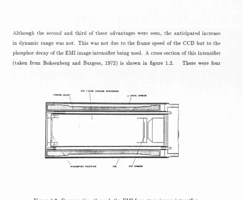
phosphor decay of the EMI image intensifier being used. A cross section of this intensifier
(taken from Boksenberg and Burgess, 1972) is shown in figure 1.2. There were four
EMI t s u c c CASCADE MIENSIEKM
C O a iN O JACKEI » .M E IA A S M EE M
M IE N S » IE M FACEPVAIE COE EXIT WIMOOW
Figure 1.2: Cross section through the EMI four stage image intensifier
phosphors altogether in the intensifier and this meant th a t the final output phosphor
decay was much longer than th a t of a single phosphor, being 3ms to 10%. On fast frame
rates the phosphor decay was causing problems. Double counting was being seen with some
events due to the same event being detected in contiguous frames. Although the event
discriminator threshold could be raised to minimise the double counting, it m eant th a t
d ata was being lost due to the rejection of smaller events. Nevertheless, the detector was
successfully developed and an engineered system was built for the 4.2m William Herschel
Telescope (W HT).
The incorporation of a CCD in place of the TV camera required a substantially different
system. A block diagram of the system is shown in figure 1.3. In particular, there were
a num ber of im portant features built into the system.
• Because the CCD physically had a small number of pixels, the system would only
have had a very small format unless the technique of interpolative centroiding had
AMP.
QU» tpb
H tA O
r
i j = t > ç a
w rit» ^
OISPIA T t o
DISK C}=
IA P € ;J=U
O A T A P R O C E S S O R
I p i A t î n couNrcRl
ACQUISITION
C O M P U T E R S Y S T E M
Ooto
Figure 1.3: Block diagram of the CCD-IPCS
been employed. This technique, which is described in section 6.6.3, finds the position
of the centre of an event by looking at the shape of the profile of photon events as they
appear on the output phosphor. In the CCD-IPCS, electronics were incorporated
into the system to centroid in both the X direction and the Y direction giving a
form at of 3072x2304.
• There were two sources of noise present in the system th a t required the incorporation
of two sets of scan coils surrounding the EMI intensifier. By moving the prim ary
photoelectrons in a controlled manner across the detector and then correcting for
the movement within the processing electronics, a technique known as ‘dithering’,
the two noises could be minimized. The two noise sources were
— the granularity associated with the grains of the first of the four phosphors,
- the fixed pattern noise th at resulted from errors in the im plem entation of the
interpolative centroiding technique.
# It was necessary to incorporate a frame subtraction circuit into the system. This
required a frame store circuit. Frame subtraction was performed for two reasons,
— to remove the double counting caused by the phosphor decay,
— to remove the CCD dark current which provided a pedestal upon which the
event d a ta sat. This DC bias was variable across the CCD due to the inherent
tim e differences associated w ith reading out different areas of the CCD.
Fram e subtraction did lim it the dynamic range, however, since losses occurred when
two events arrived in contiguous frames in the same location.
• It was necessary to correct for the charge transfer inefficiency of the CCD. Small
am ounts of charge are left behind when CCD pixels are read out of the device
by charge transfer, which is described in section 5.1. This changes the shape of
the photon event as seen by the processing electronics and results in errors in the
centroiding. By incorporating a charge transfer inefficiency (C TI) correction circuit
this effect could be accounted for.
• A ‘p artial scan’ facility was incorporated into the CCD cam era electronics in order
to achieve spectroscopic form ats and reduce the frame tim e, thus increasing the
dynamic range.
Im portant performance characteristics of the CCD-IPCS are
Resolution 25/xm averaged over the field
Q uantum efficiency 14%
Dynamic range Spectroscopic form at 7 counts pix“ ^ s“ ^
Full form at 1 count pix“ ^ s“ ^
Time resolution 1.6ms on a form at of 3072x32
1.2.3
T he M icroChannel P la te Intensified C C D Im age P h o to n C ounting
D e te c to r (M IC -IP C S)
The MIC-IPCS (MIC) (e.g. Fordham et al., 1990, Fordham et al., 1991) was the next
update in the UCL development of photon counting systems.
The deficiencies of the CCD-IPCS were associated with the EM I intensifier b ut, at
of Science, Technology and Medicine (ICSTM ) were collaborating w ith the Royal Green
wich Observatory (RGO) and Instrum ent Technology Limited (ITL) in order to develop
a microchannel plate (M CP) intensifier specifically designed for photon counting applica
tions. Compared to the EMI intensifier, the M CP would provide higher dynamic range,
be more compact and would have a lower power consumption. These advantages are
discussed in detail in chapter 3. Essentially, the processing electronics developed for the
CCD-IPCS were used with the new MCP intensifier and this system became the ground
based MIC-IPCS (MIC).
There was another im portant innovation th a t distinguished MIC from the CCD-IPCS
and th a t was the incorporation of fibre optic coupling from the intensifier to the CCD
in place of lens coupling. The fibre optic tap er provides a high transfer efficiency and
compact optical coupling w ithout the optical aberrations associated w ith lenses. This
innovation is discussed in detail in chapter 4.
W ith the two new components discussed above the prototype MIC photon counting
detector had become a very compact, lightweight system having the following performance
characteristics.
Resolution 27/i/m
Q uantum efficiency 14%
Dynamic range Spectroscopic form at 20-40 counts p ix ~ ' s” '
Full form at 2 counts p ix ~ ' s“ '
Time resolution 1.6ms on a form at of 3072x32
The following chapters describe the design, operation and performance of a version of
C h ap ter 2
T h e Space B ased M IC
The previous chapter described how 20 years of development in photon counting detectors
a t UCL led to the development of the ground based MIC system. Successive changes to
the original IPGS have led to the development of a highly com pact, lightweight system
suitable not only for large telescope applications, but also for small telescopes and, in
particular, space applications.
However, the ground based and space based environments are sufficiently different
th a t it is not possible simply to use the ground based MIC for space applications. For
example, there are very strict power and space constraints placed upon any space based
system so th a t only the essential features of the ground based system can be included in
a space version. Also, the performance characteristics required of a space system are not
necessarily the same as those of a ground based system. In this respect new features may
need to be included into a space system or some features of the ground based system may
not be needed. Although the main features of the ground and space based systems are
essentially the same, the num ber of differences between the two make them very distinct.
In particular, some differences between the ground based MIC and the space based
MIC are:
• The ground based MIC uses d ata about an event contained in 5 pixels in order to
perform centroiding. For the purposes of lowering power consumption, the space
version of MIC uses 3 pixels of data.
• Also for the purposes of reducing power consumption, the processor uses high speed
• The frame subtraction circuit is no longer needed because the CCD dark current, or
DC bias, is removed in the CCD camera before it reaches the processing electronics.
• The charge transfer inefficiency correction circuit is no longer needed because the
transfer efficiency of modern CCDs has become so high. Again, removing it lowers
power consumption.
In addition to these changes outlined above, which are mainly associated w ith a reduction
in power consumption, there are changes associated w ith the intended application which
is described shortly. For example, only a portion of the CCD is used and, furtherm ore, a
facility has been included for reading out only selected areas of the CCD. O ther changes
to the space system compared to the ground based system will become apparent when a
description of the space system is given.
2.1
T h e A p p lica tion o f a Space B ased S y stem
The development of a space version of MIC was funded from two sources.
• The European Space Agency (ESA) provided funding for the development as p art of
th e Boresight Faint S tar D etector (BFSD) project. Here, the intended application
of the system would be as an optical m onitor (OM) operating at visible and UV
wavelengths on a spacecraft where the prim ary telescopes operate at non-visible
wavelengths. This would allow the same objects to be viewed simultaneously at
different wavelengths.
• The Science and Engineering Research Council (SERC) provided funding for the de
velopment of a space version of MIC as the optical m onitor on the X-ray M ulti-m irror
Mission (XMM) which is an ESA ‘Horizon 2000’ space observatory due for launch in
1998. Here, the prim ary telescopes operate at X-ray wavelengths. Figure 2.1 shows
how the XMM satellite might look with the three prim ary X-ray telescopes clearly
visible and the optical m onitor as indicated.
The system described in the remaining chapters was designed to meet the requirements
of the XMM project, although a system designed for the BFSD project would be very
SOiAR ARRAY
Figure 2.1: The XMM spacecraft showing the location of the optical monitor
2.2
Scientific R eq u irem en ts o f th e X M M O ptical M onitor
The XMM-OM will have two detectors, the red camera which is a CCD camera operating in
the range 6500-10000Â and the blue camera which will be the photon counting detector
operating in the range 1500-6500Â. The primary scientific requirements of the photon
counting detector upon which the development of the XMM-MIC has been based (Mason,
1989) are summarised in table 2.1.
The Zodiacal light background will be 0.2 counts s~^ arcsec” ^ and the detector must
be able to detect the target objects in the presence of this background. The 3a detection
limit means th a t the detector m ust be able to detect a 24 m agnitude star to 3a above
the background in 1000 seconds. This magnitude is equivalent to a flux of 0.04 counts
s“ ^ arcsec"^ and represents the faint limit of the detector’s performance. The brightest
star observable should have a m agnitude of 13.2 for white light - this is equivalent to
1000 counts s~^ arcsec—2 and represents the bright limit of the detector’s performance.
The detector dark noise should be no greater than 4x1 0"^ counts s~^ arcsec"^. This
requirement is not so im portant for a space version of MIC because the Zodiacal light
Table 2.1: Prim ary scientific requirements of the photon counting detector for XMM W hite Light
(1500-6500Â)
B-band
Zodiacal light background (s“ ^ arcsec"^) 0.2 0.04
3(7 detection lim it in 1000 s (equiv. B mag.) 24.0 23.0
Brightest star observable (Mag.) 13.2 12.0
D etector dark count (s“ ^ arcsec"^) 4x10⁻⁴
D etector lifetime 10 years
background will dom inate the background signal in the detector. The detector lifetime
should be ten years which means th a t it should still be operating after this period.
In addition to these requirements the detector should have a 16 arcmin field of view
w ith a resolution of 1 arcsec. If one allows two pixels per resolution element then the
detector characteristics shown in table 2.2 can be derived. A nother requirement of
Table 2.2: Required characteristics of the XM M -M IC D etector resolution <20fim FWHM
Pixel scale 1 pixel = 0.5 arcsec
Diam eter of active area 25mm
Active detector area 18.94mm X 18.94mm
No. of pixels in detector form at 2048 X 2048
Pixel size 9.24^m
the XMM-MIC is a hardw are ‘windowing’ facility whereby up to 16 user definable d ata
acquisition windows can be placed within the 2048x2048 detector form at. This facility is
required for two reasons.
• Memory lim itations prevent d ata acquisition on the full 2048x2048 form at.
• To enable d a ta acquisition on a num ber of ‘guide sta rs’ w ithin the detector full
form at. These will be used for measurement of telescope tracking and roll errors
d ata associated with the guide stars will be time sliced into 10-50 second exposures.
The image of each guide star in each time slice is then software centroided and its
position compared against a datum defined at the start of the integration thus giving
a measure of image movement. These d ata are then fed to correction mechanisms
in the red camera to m aintain imaging resolution on th a t camera. This tracking
facility is required as the imaging resolution of the XMM-OM will be higher than
th a t of the X-ray telescope and hence of the spacecraft guidance system.
Figure 2.2: An example of the use of the windowing facility. D ata are only acquired in
the four windows A -D . Window A might be used to acquire scientific data while windows
B-D would be used for star tracking
Up to 10 of the 16 windows will be used for guide star d ata acquisition leaving 6 free
for scientific purposes. An example of the use of the windowing facility is shown in
figure 2.2. A part from being a requirement of the XMM-OM MIC, the windowing facility
also provides a means of increasing the dynamic range of the detector. The way in which
this is achieved will be discussed in section 5.3.2.
2 .2 .1 O v e r v ie w o f t h e X M M -M I C
To best meet the requirements and characteristics described in the previous section, the
XMM-MIC was designed. A block diagram of this system is shown in figure 2.3 and a
F ib re
T a p e^ V ideo
A m p. CCD
E v e n t A d d ress
W indow fo rm at
8 bit ADC EHT Supply CPU Memory Integrated Display 25mm MCP Intensifier Data Processor CCD Controller
Figure 2.3: Block diagram of the XMM -M IC
photograph of the system is shown in figure 2.4. The photograph shows various compo nents of the system depicted in figure 2.3, the detector head, comprising intensifier, fibre tap er and the CCD w ith its associated electronics is m ounted on the optical bench on the
left w ith a real tim e display beneath it. To the right of th a t is the com puter, comprising
CPU and memory, w ith the image processing chassis, or d ata processor, on top of th a t.
On the far right is the m onitor th a t allows real tim e viewing of the integrated image.
The most crucial element of the system is a 25mm diam eter microchannel plate (M CP)
image intensifier. The intensifier converts an incoming photon to an electron, produces
electron m ultiplication and then converts the resulting electron pulse into a light pulse,
or photon event containing ~10^ photons. An EHT power supply provides the potential
differences w ithin the tube necessary to produce the electron m ultiplication. The spatial
position of the incoming photon is preserved during the intensification process so th a t the
output is essentially an amplified image of the input.
The light o utpu t from the intensifier is coupled via a 3.06:1 reduction fibre optic taper to a fast scanning CCD. The CCD has a usable area of 256x256 pixels w ithin its to tal array of 384x288 pixels. P hoton events th a t are output from the image intensifier are captured within the imaging area of the CCD.
The raw video signal from the CCD is amplified, processed and digitized by an 8-bit
‘flash’ analog to digital converter (ADC) before being passed onto the image processing
electronics. These processing electronics recognise photon events, centroid them to within
CO l\5
î | «
d ata contained in the memory are shown as an integrated display on a m onitor so th a t
the d a ta m ay be viewed as they are coming in.
Software control of the system is provided by th e CPU. In particular, the CPU calcu
lates th e window form at to be used for a particular integration and loads the inform ation
into the CCD controller which controls the reading out of the CCD.
Two features of the system described above which are unique to the XMM-MIC are:
• The hardw are windowing facility described in the previous section th a t is incor
porated into the CCD controller to allow up to 16 user definable d a ta acquisition
windows to be placed within the 2048x2048 detector form at
• A m ultiple event discriminator circuit incorporated into the processing electronics.
This recognises when there is more than one event present at the same place on the
CCD, This facility helps to increase the dynamic range of the detector by increasing
the m aximum detectable count rate. A full description of the circuit is given in
section 6.5.
Also, in common w ith the ground based MIC, the XMM-MIC has a resolution select circuit
th a t enables the maximum form at to be 2048x2048 w ith 9/im pixels or 1024x1024 with 18/xm pixels.
The following chapters describe the design and operation of the various components
of the XMM-MIC. The overall performance characteristics of the detector to date are
C h ap ter 3
T h e Im age Intensifier
3.1
In trod u ction
The image intensifier is the most crucial component of the system. It detects individual
photons and intensifies them, producing a splash of photons at the output th a t is visible
even to the naked eye. It retains the spatial position of the detected photons so th a t the
output is essentially an intensified image of the input. Each splash of photons, or photon
event, at the output is conveniently detected by a CCD reading out many frames per
second.
Photon
Electric field
photon event
Input Window j 3 MicroChannel Plates
j
Fibre FaceplatePhotocathode Phosphor Screen
Figure 3.1: Schematic of the various stages of the MCP intensifier
The image intensifier used in MIC is a 25mm diam eter microchannel plate (M CP)
intensifier. A schematic of the various stages of the intensifier is shown in figure 3.1.
Photons enter the intensifier via an input window and strike the photocathode. The
photocathode em its an electron which is accelerated under the influence of an applied
potential and enters a pore of the first of three microchannel plates arranged in a Z-
configuration. Each microchannel plate is a wafer of semiconducting lead glass w ith >10®
microscopic pores extending from the input face to the ou tput face. These pores are
capable of electron m ultiplication when a potential is applied across them . A cloud of
~10® electrons emerges from the last channel plate and is again accelerated by an applied
potential to strike a phosphor screen. The phosphor em its around 10^ photons, which
constitute a photon event, and these emerge at the intensifier ou tp ut via a fibre optic
faceplate.
Previous UCL photon counting detectors, the IPGS (e.g. Boksenberg and Burgess,
1972) and the CCD-IPCS (Fordham et al., 1986), used an EM I m agnetically focussed four
stage image intensifier. These intensifiers had high gain and high resolution, as is ideally
required of photon counters, but they also had a num ber of undesirable characteristics.
However, towards the end of the CCD-IPCS development. Im perial College of Science,
Technology and Medicine (ICSTM ), The Royal Greenwich Observatory (RGO) and In
strum ent Technology Limited (ITL) had been developing an M CP intensifier specifically
designed for photon counting applications. This intensifier offered the following advantages
over the EMI intensifier.
• The EMI intensifier was lim iting the system ’s dynamic range. The four stages within
the intensifier, each w ith a phosphor screen, were resulting in a very long output
phosphor persistence of around 3ms to 10%. On fast frame rates this was causing two
problems. Firstly, w ith the CCD-IPCS, not enough charge was being accum ulated on
the CCD in single frames which m eant th a t not m any events were being detected.
Secondly, on slower frame rates, a high percentage of detected events were being
counted twice. This second effect required the im plem entation of a frame subtraction
circuit to remove the second event but this then resulted in an additional source of
coincidence loss whereby the second of two real events th a t arrived in the same place
in contiguous frames was being lost.
elimi-nate lost events and double counting since all the photons em itted by the phosphor
would arrive at the CCD in the same frame. A gain in dynamic range would then
be possible w ith the use of the MCP intensifier in place of the EMI.
• The EMI required an external magnetic focussing field which was provided by a
coil surrounding the intensifier body. The coil consumed a lot of power, made the
intensifier very bulky and heavy and dissipated a lot of heat which required a large
portable cooler to be incorporated into the system. These factors effectively limited
the detector’s applications to large telescopes.
The MCP intensifier is physically very compact and requires no external magnetic
fields which considerably reduces its size, power consumption and heat dissipation.
This enables the detector to be used for applications where there are space and power
constraints such as on small telescopes and in space.
• The magnetic focussing of the EMI intensifier introduced a characteristic distortion
known as S-distortion which had to be removed by software during d a ta reduction.
The absence of a magnetic field in the M CP intensifier m eant th a t there was no
distortion in the image.
• The EMI intensifier, which was a commercially available product, was not stan
dardly available with a choice of photocathode or input window which restricted its
use to one wavelength range. The M CP intensifier is available w ith a choice of pho
tocathodes, for example, S-20, bi-alkali or gallium arsenide, and a choice of input
window, for example, magnesium fluoride, sapphire, Suprasil and ZKN7. W ith a
suitable choice of photocathode and input window any num ber of wavelength ranges
becomes possible.
In addition, the M CP intensifier has a desirable pulse height distribution which makes it
superior to the EM I for photon counting.
UCL collaborated with ICSTM and ITL on the development of MIC, incorporating
the M CP into the CCD camera system developed for the CCD-IPCS. The XMM-MIC is
a compact, low power version of th a t original MIC. The intensifier has certain features
th a t make it ideal for photon counting and for use in a space environm ent. The design
3.2
T h e D esig n and O p eration o f th e In ten sifier
The image intensifiers for the prototype XMM-MIC have been supplied by two sources.
ITL have m anufactured two and a th ird is in production at Delft Electroniche Producten
(D E P). The intensifiers have been designed as far as possible to meet the requirements
for XMM shown in table 2.1 in term s of resolution, detective quantum efficiency (DQE),
dark count and maximum count rate. Figure 3.2 shows a photograph of the intensifier;
|c m
I
Figure 3,2: The 25mm microchannel plate image intensifier
the small size of the intensifier is indicated by the centim etre scale. A schematic of a
cross section of the intensifier incorporated into the detector head is shown in figure 3.3.
The various components of the intensifier shown in the figure and their functioning are
described in the following sections.
C eram ic
b o d y E le c tr o d e co n n e c tio n s
F ib r e -o p tic o u tp u t p la te
F ib r e -o p tic ta p e r 3.06:1
C en tro id in g E lec tro n ics
25m m p la te s
T h o m so n T H 7 8 6 3 C C D
In p u t w in d ow S ap p h ire
P 2 0 C a th o d e P h o sp h o r
8 2 0 C a th o d e
Figure 3.3: Schematic of a cross section of the intensifier incorporated into the detector
head
3 .2 .1 T h e I n p u t W in d o w
The input window serves two purposes:
• Its inner surface has the photocathode deposited directly onto it.
• It is used to form a vacuum seal with the intensifier body.
Together with the photocathode the input window determines the spectral response of the
intensifier. The choice of window m aterial determines the transm ission of the window to
various wavelengths.
The required wavelength coverage of the detector, 1500-6500Â, lim its the choice of
m aterials to either sapphire or MgFg. The transmission of these two m aterials in this
range is shown in figure 3.4. Although M gF2 has higher transm ission, both ITL and
DEP report th a t the deposition of a photocathode onto this m aterial presents problems.
In particular, photocathodes deposited onto MgFg tend to have a spatially non-uniform
&
c
o
U) V) B
V)
C cO S-, E—'
100
MgF;
8 0
60
40 S a p p h i r e
200 3 0 0 4 0 0 5 0 0 6 0 0
W a v e l e n g t h ( n m )
Figure 3.4: Transmission of M gF2 and Sapphire windows
responsive quantum efficiency (RQE). The RQE of a photocathode is the percentage of
incident photons th a t give rise to an em itted electron. A consequence of the difficulty of
depositing photocathodes onto MgF2 is th at photocathodes deposited onto sapphire have
consistently shown higher RQE, typically by 30%, compared to the same photocathode
on M gF2.
The two intensifiers supplied by ITL were m anufactured with sapphire windows because
they wished to widen their experience to include knowledge of deposition onto sapphire
as well as on M gF2- This also allows a comparison of photocathode response using two
window types since d ata already exist for M gF2. The ‘hot seal’ technique used by ITL
initially was not useful for sapphire windows because the high therm al conductivity of
sapphire resulted in a dry joint using an indium-tin solder. An indium -bism uth solder,
which has a higher melting point, was used to solve the problem.
The sapphire windows have the undesirable characteristic th a t they fluoresce when
bombarded by radiation, as discussed by Oldfield (1991). The contribution from radioac
tive isotopes within the window m aterial and from cosmic rays leads to frequent ‘flashes’
seen at the intensifier output.
As yet, the choice of input window has not been decided and more d ata are needed
before a final choice is made.