5783
Transaction Level Modeling (TLM) of Secure
Digital Input Output(SDIO) Protocol
Khaja Mujeebuddin Quadry, S. P. Venu Madhava Rao, Nafiza, Fathima Zaheera
Abstract The SD memory card offers high speed input/output (IO) data with emphasis on less power consumption particularly for mobile
phones, PDA, Palm tops etc. In this paper the Transaction Level modeling of the Secure Digital IO protocol has been done. The aim of a transaction-level model is to represent the functionality of a design efficiently and faithfully, in a way that is simple to write and simulate. The Transaction Level Model developed will be useful for verification and thereby implementation.
Bus functional models designed using Transaction level modeling (TLM) are also helpful to debug the test benches. Transaction level modeling (TLM) of secure digital IO protocol is done using System Verilog [3], as System Verilog offers all the necessary features and constructs for writing transaction-level models. The simulation is carried out with synopsis VCS tool.
Index Terms— Bus functional model, Secure Digital card, Simulation, System Verilog, Transaction, Transactor, Verification.
—————————— ——————————
1 I
NTRODUCTION HE Secure Digital (SD) Memory Card is specifically designed to offer the security, performance, capacity, and environment requirements of newly emerging video and audio consumer and commercial electronic devices. SD Cards are used in different available digital products, cellular phones, digital music players, digital cameras, handheld PCs (HPCs), smart phones, digital video camcorders, electronic books and car navigation systems. SD Host Controller acts as the interface between SD Memory card and the host system. SD Host Controller communicates with host system for example ARM processor using AMBA AHB, and also communicates with SD memory card using SD IO protocol [1], [2]. Transaction Level abstraction is used for verification of functionality as this is more efficient from the debugging, performance point of view and also in terms of time required for simulation as compared to doing low level bit_twiddling operations on individual signals in Register Transfer Logic (RTL). A properly designed transaction-level model will only take less amount of time compare to design an RTL model, thus enabling the verification and design team to work simultaneously or in parallel thus reducing the time to market. TLM model also executes faster than the RTL model by some orders of magnitude, this allows the tests and verification environment to be designed and debugged very much faster. System Verilog [3] is often used as modeling language for Design methodologies to write a transaction-level model of the design under test, as it offers all of the necessary high-level features and constructs that make more efficient for the design of transaction-level models [4], [5], [6].A transaction abstracts the set of data (logical set) that is transferred between the blocks. It does not have notion of time and triggers an event once it is kept on the bus. A transactor concurrently executes the tasks that monitor (watch) and drive a transaction (assign). A driver transactor is used actively supply the data to the design under test (DUT) and can be either a reactive driver or a proactive driver. A proactive driver will control of the initiation and type of transaction. Whenever a new transaction is given by the higher layers of
design verification environment, the transaction is immediately put or executed on the physical interface. A reactive driver will not be in control of type of transaction or initiation but may be in control of some aspect of its execution timing, such as wait states introduction. The design under test (DUT) initiates the transaction and the required data is supplied by reactive driver to successfully complete the transaction [4], [5], [6].
A monitor is used to report the observed timing of transaction and data information at high-level. A reactive monitor consists elements to generate the necessary low-level signals used for handshaking to complete a transaction successfully. A passive monitor reports by observing all the signals that are involved in transaction without any interference. In a system level design and verification environment a passive monitor is used for monitoring transactions on an interface between two design under test (DUT) blocks. Transactor consists of variables, components and ports of the verification environment that are used or to generate protocol transactions or acts as interface for a particular protocol between two levels of abstraction. In the order of thousands of transactions generated by the generators, communicate through transactors, get recorded and comparison also performed then freed. Transactors are better modeled using a transaction descriptor. A transaction description contains all of the required information to invoke the appropriate procedure that implements the transaction [4], [5], [6].
Dongwan Shin et al. [7] proposed a method based on virtual architecture models to generate transaction-level models in which blocks communicate via abstract information-passing channels. Lukai Cai et al. [8] proposed several TLMs and presented the system level design flow and also major design tasks for generation of each model. Aisha Bushager et al. [9] presented smart card security protocol modeling using The Unified Modeling Language (UML) 2.0. SystemC is used to program executable model using Transaction Level Modeling (TLM). Soha Hassoun et al. [10] presented layered architecture suitable for both emulation and simulation. The architecture uses transactions for synchronization and communication and
5784 between the device under test (DUT). And driving
environment (DE). Krste Asanovi´c et al. [11] presented transactor model for both hardware and software implementation using natural level of design representation.
2
DESIGN
OFS
ECURED
IGITALIO
T
RANSACTOR The SD IO protocol is implemented as a 9-pin serial interface and supports up to 4 data pins. It is a synchronous interface with the clock being provided by the host device. Bi-directional command and data buses are used and are implemented in a dominant-recessive manner such that the buses are pulled-high when not active. The maximum clock frequency is 25MHz and as such the maximum data transfer rate is 100Mbps [1], [2]. Commands and data are transferred in frames with start-bit, stop-bit and CRC fields as shown in Fig 1. The protocol is implemented in System Verilog[3], as per the definitions [1], [2].Fig 1. Command Response Signals
Based on the functionalities the SDIO Transactor has been divided into two types:
1. Monitor 2. Drive
The monitoring function is again divided in to three tasks 1. Monitor command response
2. Monitor data0-data3 lines for read and write data and CRC status &
3. Monitor interrupt on data1 line
System Verilog [3] Code Template of the bus functional model for secure digital IO protocol is given below. The drive and monitor transactors are implemented as tasks.
`include "KmqDefines.svi"
`include "KmqSdIoTransaction.svi" `include "KmqSdIoTransactor.svi"
function KmqSdIoTransactor::new(string name);
endfunction : new
task KmqSdIoTransactor::init(virtual KmqSdIoInterface SdioIntf);
endtask: init
task KmqSdIoTransactor::reset(); endtask: reset
task KmqSdIoTransactor :: run (); endtask:run
task KmqSdIoTransactor :: drive (); endtask : drive
task KmqSdIoTransactor::send(KmqSdIoTransaction driveIo);
endtask: send
task KmqSdIoTransactor::monitor (); endtask : monitor
task KmqSdIoTransactor ::
monitorIoBusforCommandResponse ();
endtask : monitorIoBusforCommandResponse
2.1 Monitor Command Response Task
In the absence of command and response, the command response line is pulled high. This task always monitors command response line.
Fig 2. Flow chart Command Response Task
If the line goes low detects the start bit, and then captures the second bit (direction bit) if it is 1 starts capturing first 6 bits (command Index), 32 bits argument, 7 bits CRC, then calculates CRC and compares with the received CRC Then sets the CRC Validated bit if matched. It finally captures end bit and checks whether it is 1 or not if it is not 1 it is the indication end bit failed. The Fig. 2 gives a detailed flow chart representation of the command response task. After capturing command index the parameters needed to capture response ————————————————
Dr. Khaja Mujeebuddin Quadry, Professor ECE, Siddhartha Institute of
Technology & Sciences (SITS), TS, India.mail: [email protected]
Dr. S. P. Venu Madhava Rao, Professor ECE & HOD
MVSREC, Hyderabad, TS, India. mail:[email protected]
Nafiza, AssistantProfessor ECE, Siddhartha Institute of Technology &
Sciences (SITS)TS,India. Email: [email protected]
Fathima Zaheera, AssistantProfessor ECE, Siddhartha Institute of
5785 Start 1 1 1 detected 0
0 start bit detected Serial bit s tream Dat a0 line 1bit / 4 bit mode
Capture
Data
Capture
CRC 16 bits
Capture
end bit
Calculate
CRC 16 bits
Compare CRC
Is end bit 1
If Yes End bit detected If NO
End bit Failed
Go bac k t o start
If ok crcValidat ed =1 Else crcValidated =1 Data length, 1bit /4bit mode
is set by Command response task
is data Expected
=1
yes
no Card model is bus y Club 4 line
data to single line
and data are set according to the commands received. For example if cmd2, cmd9, cmd10 received then response length is set to 136, else 48 bits. For data commands data expected bit is set, read or write data is also identified from the commands. Data bus width 1bit or 4 bit mode is set if Acmd 6 is received. The functionality is implemented from the card specifications [1], [2]. Now if the captured direction bit is 0, starts capturing first 6 bits response index, argument either 32 bits or 120 bits set by command, 7 bits CRC , calculates CRC for direction, index , argument concatenated and compares with the received CRC, sets the crcValidated bit to 1 if matched, Finally checks for end bit if 1 gives message response end bit detected, else gives message response end bit failed. Again starts monitoring for start bit.
2.2 Monitor data0-data3 lines for read and write data and CRC status Task
In the absence of data on data lines all lines are pulled high, data starts with start bit 0, 16 bit CRC, followed by the data, finally end bit 1 comes last and the data line pulled high as shown in Fig.3 below.
Fig. 3.Data signals on 4 data lines
The Fig. 4 shows the flow chart for monitoring the data on the four data lines as the data lines are connected to pull up in the absence of data, The data monitor task starts looking for a 0 (low start bit ) on the data line , checks for data expected bit, If high starts capturing 1bit/ 4 bit data , depending on the 1 bit or 4 bit mode , data length to be captured is set by command response task. Once data capture over starts capturing CRC 16 bits for every data line, calculates the CRC and compares with the received CRC set crcValidated bit to 1 if both are matched , for 4 bit mode after capturing data 4 lines of data is clubbed together to get the single line data. Identifying read or write data is done from the bit is write data set by the command response task. As after capturing data all data lines are connected to pullup, for write data secure digital card sends back either 010, or 101, preceded by start bit followed by end this is also captured by the task.
2.3 Driving response Task
After receiving the transaction from the card model the drive response task checks the data type, if it is 01 then starts driving start bit, response, calculates CRC and drives, finally drives the end bit, and go back to wait until transaction received.
2.4 Drive Read data and CRC status
The flow chart for the drive read data and CRC status is as shown, The task stays in the loop until the transaction received from the card model , after receiving transaction checks the data type if 10 starts driving the start bit for read data , 1bit mode or 4 bit mode is set by the command response task, drives the read data, the data length to be driven comes along with the transaction, calculates the CRC for the data, drives the CRC, end bit and comes back to the begin of the task. If data type received is 11 then drives the start bit then CRC status and end bit on to the data0 line for both 1 bit or 4 bit mode.
Fig 4. Flow chart Monitor data0-data3 lines for data and crc status
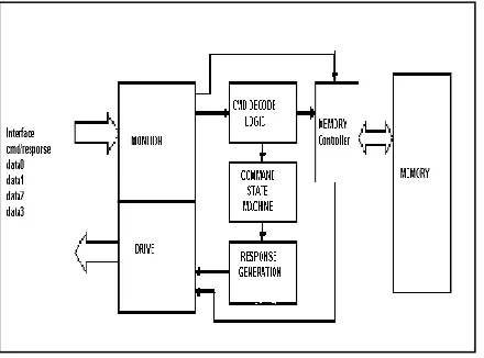
3 SECURE
DIGITAL
(SD)
D
EVICEM
ODEL5786 the command state machine gets updated according to the
received command. If command received for write operation memory controller gets address block length from Command Decode Logic block, writes the data received in to the memory. It checks the crcvalidated bit in the transaction and sends the CRC status to the drive task.
When card model receives the command for read operation memory controller gets address, block length from command decode logic sends the Data transaction to the drive task of IO transactor from the corresponding address.
Fig. 5. Block Diagram of SD Card model
4 S
IMULATIONR
ESULTSThe results of simulation are stored in the log file with reference to the simulation time for different test cases. Also wave forms of the signals are dumped which are further useful for analyzing the failure cases.
Fig 6. Single Block Write and Read from the SD card
Simulation results for some of the test cases are shown in the Fig 6. Test cases are written to test all the commands and responses of the SD Memory card also to complete the code coverage.
5
C
ONCLUSIONThe feature of System Verilog [3] are used efficiently to make our verification environment more reusable and manageable and the scheme of constrained-randomization method of stimulus generation helped us reduce a lot of redundant man efforts without any quality degradation. The detection of bugs achieved in the phase of randomization, directed tests detected only a less amount of bugs that are occurred in corner cases. The most importunately the information generated from our verification environment helps the design engineers to fix these bugs quickly thus helps in reducing the time to market.
Transaction level modeling (TLM) ensures raising the level of design abstraction. These models communicate with each other with the interface at the transaction level. Working with TLMs achieves architectural exploration and there by allows system engineers to perform validation, co-verification and hardware/software integration.
Even though most of the verification goals are achieved here, still some important improvements need to be added in future. Assertion statements are to be added separately to to make sure that the interface is compliant to its own specifications or not, also assertions help in monitoring some critical timing relationships and components for various kinds of sequences that appear on the interface.
R
EFERENCES[1] SD Specifications, Physical Layer Simplified Specification Version 2.0, Part 1, SD Group, SanDisk Corporation & Toshiba Corporation, 2006.
[2] SD Specifications, Part A2, SD Host Controller, Simplified Specification, Version 4.2, 2017.
[3] IEEE Standard for SystemVerilog—Unified Hardware Design, Specification, and Verification Language, IEEE Computer Society and the IEEE Standards Association Corporate Advisory Group, 2017.
[4] Verification Manual for System Verilog, Janick Bergeron, Eduard Cerny, Alan Hunter and Andrew Nightingale, Springer, 2006. [5] Writing Test benches using System Verilog, Janick Bergeron,
Synopsis Inc, Springer, 2006.
[6] Functional Verification of HDL Models, Janick Bergeron, Qualis Design Corporation, Kluwer Academic Publisher, 2000.
5787 System Synthesis (CODES+ISSS '06).
[8] Lukai Cai and Daniel Gajski ―Transaction Level Modeling: An Overview‖ First IEEE/ACM/IFIP International Conference on Hardware/ Software Codesign and Systems Synthesis (IEEE Cat. No.03TH8721).
[9] Aisha Bushager ; Mark Zwolinski,‖ Modelling Smart Card Security Protocols in SystemC TLM, 2010 IEEE/IFIP International Conference on Embedded and Ubiquitous Computing.
[10] Soha Hassoun, Senior Member, IEEE, Murali Kudlugi, Duaine Pryor, and Charles Selvidge, ‖A Transaction-Based Unified Architecture for Simulation and Emulation‖ IEEE transactions on very large scale integration (vlsi) systems, vol. 13, no. 2, february 2005.pp. 278–287. [11]Krste Asanovi´c, ‖Transactors for Parallel Hardware and Software