Substrate Temperature Effects on Optical Properties and Constants of
ZnO
Ban A. Badr1, Qamar Q Mohammed2, Najwan H. Numan3, Makram A. Fakhri3* and Ahmed W. Abdul Wahhab3
1 Physics Department, collage of Education, University of Al-Hamdaniyah. Iraq. 2Control Eng. Dep., University of Technology, 10066 Baghdad, Iraq.
1Laser and Optoelectronic Department, University of Technology, 10066 Baghdad, Iraq.
Received 16 August 2018, Revised 31 October 2018, Accepted 12 February 2019
ABSTRACT
The preparation process of ZnO TCO (Transparent Conducting Oxide) thin films have been conducted in this paper. A Q-switched Nd:YAG laser of 7 ns duration and 1 joule of energy was utilized to perform the deposition process of ZnO/glass heterojunction. Up to the optimum oxygen pressure, optical constant and properties of the prepared samples have been investigated. Under oxygen ambient of 300 torrs and without post-deposition heating treatment, the results recorded an electrical sensitivity of 0.0221 Ω.cm. higher transparency of 80% was also listed with a reduction in its value alongside with the reduction of the substrate temperature. Further, the energy bandgap has found to be 3.46 electron-volts.
Keywords: TCO Thin Film, PLD Deposition, Optical Properties, ZnO.
1. INTRODUCTION
Historically, the beginning of the 20th century was reported the first preparation of transparent conducting oxide (TCO) thin film. Since that time, it goes under significant developments and considered as one of the most important materials that can be seen in everyday applications such as displays [1-7]. The low resistivity of TCO thin film is the most powerful electrical properties (high conductivity) alongside with high transparency in the visible region of the optical spectrum [8-11]. Such distinguished electrical and optical properties of this material were seen as a highly qualified material to be used in a wide range of optoelectronic applications. Zinc Oxide (ZnO) is one of the transparent conducting oxides that got attention because of its distinct properties. Large band-gap, high conductivity, and high thermal and chemical stability are some of ZnO properties [12 – 18]. With such properties of interests, the ZnO thin films mastered the commercial and scientific research fields.
In order to obtain good piezoelectric characteristics, the ZnO films have to be foremost crystallizing in form of quartzite structure. Therefore, the c-axis orientation of the ZnO thin films is becoming a beneficial material used to prepare bulk and surface acoustic-wave devices [19-20]. Besides, wide band-gap of zinc oxide shows a superb transparent material in the range of visible and ultraviolet spectrum. In addition to its lower toxic effect, it becomes an exemplary element enters in the production of ultraviolet blocking sunscreen.
284
According to the deposition conditions, in term of substrate temperature and oxygen pressure, the zinc oxide thin films can be classified into three different groups. Firstly, conductive and opaque film group where the ZnO is mixed with the metallic zinc in one solvent. The second group is alike stoichiometric bulk ZnO in its composition which they are lacking conductivity (insulating) with transparent capability. However, the highest importance of groups is the third group which accumulates both higher conductive ability and excellent transparent properties [21-23]. It is worth to annotate that the electrical properties of TCO films increase effectively as a result of increasing temperature from one side and reduction of oxygen pressure from other side. The reason is of dissociation of cadmium oxide formatting of a solid solution of the metal on its oxide.
2. EXPERIMENTAL PROCEDURE
Preparation parameters Preparing the substrates (glass), row materials (high
purity Zn),
oxygen pressure range of 300
mbar Laser energy (1000
mj) and 7 ns pulse duration
deposition process under different substrate temperatures of 150, 200,
250 and 300°C
Characterization and analysis Uv-vis reults ( Transmission,
Absorption, Reflection, energy band gap, and
refractive index)
Discuses the results
Figure 1. Flowchart of the ZnO nano thin Film preparation process.
285 used to ablate the high purity (99.99% purity) zinc. To ensure an accurate ablation for the target material, a lens of 20 cm focal length has been installed in front of the laser source at the angle of incidence of 45 degrees with a rotation speed of 1 rpm. 50 laser pulses are applied to the target to perform the deposition process under different substrate temperatures of 150, 200, 250 and 300°C. All the preparations and characterization processes are presented by the flow chart in the Figure 1.
A 200 nm film thickness was optically recorded using a stylus profilometer. Other optical properties such as transmittance and reflectance were investigated between the spectral the range between 0.3µm to 1µm using double beam spectrometer. The incident photon energy as a function of the wavelength can be obtained using equation (1) [24-26]:
Eg(eV)=1240/λ(nm) (1)
where λ is wavelength. The Tauc equation (2) was used to find the energy band gap as a function of the absorption coefficient and excitation of the transmission [27-29]:
(αhν)=B (hν–Eg)r (2)
where r is a constant that can take any integer value based on the raw material and the optical transmission values αhν. B is a constant inversely proportion tit the value of r. The energy band gap value can be obtained from the intercept of both curves of (αhν)1/r versus (hν) extrapolated at (αhν)1/r =0. The examination of the absorption coefficient for all used wavelengths was found
from equation (3) [30-32]:
α=2.303(A/t) (3)
where A and t are the absorbance and the transmittance, respectively. Equation (4) explains the relation between the absorption coefficient (α) and the excitation ratio (K) [33-35]:
K = α λ / 4π (4)
Other constants such as the refractive (n), εr and εi which they relate to the real and imaginary parts of the dielectric constants, the conductivity (σ) are used to be calculated from equation (5) [36-38]:
n = {[4R / (R-1)]-K2}1/2 – [(R+1) / (R-1)] (5)
Knowing that R represents the reflectance which can be calculated from (R = 1-T-A), or from equation (6) [39-43]:
n=ns 1/2 (6)
286
3. RESULTS AND DISCUSSION
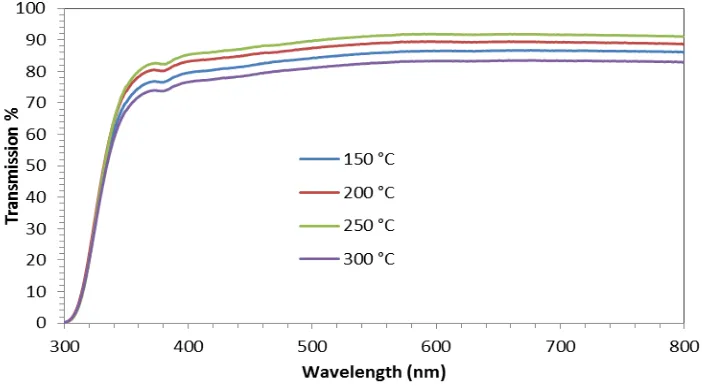
Figure 2. The Transmission curve as a function of the wavelength ranges between 300 nm to 800 nm.
Under different substrate temperatures, the transmission spectra of the prepared thin films have been examined and analyzed. Figure 2 displays the transmission of the prepared films as a function of wavelength. The Figure 2 shows that the average transmission ratio of the prepared samples increases as the temperature of the substrate goes up to 250°C then back down in 300°C as a result of effects the heating on the transparency of thin films [44]. It can be concluded that all prepared samples have high transparency at the visible region of the optical spectrum with average values reaches up to 81%. The transmission curves are found to be about 86%, 88%, 91% and 82% for 150, 200, 250 °C and 300°C of temperatures respectively. Furthermore, this change, as a result, of the improved the homogeneity and the uniformity of the structure alongside with the increasing of film thickness and the change in the grains size a very sharp cut-off is also presented at the wavelength 340 nm. Higher transmission values indicate that the prepared thin films are in crystalline form.
Figure 3. Optical absorption curve as a function of wavelengths under two substrate temperatures.
287 absorption rate with a notable shift towards lower wavelength region. This indicates that the optical energy band-gap of the prepared films is expanding.
Figure 4. The optical band-gap energy as a function of photon energy for two substrate temperatures.
Previously, we referred to Tauc equation (2) to be used for optical band-gap calculation of the prepared ZnO films. The extrapolating of the straight lines of the plot (αhv) 2 versus the photon energy given in Figure 4 is used to determine the band-gap energy. Comparing between both substrate temperatures, the difference in the band-gap energy bands is comparatively small. Table 1 gives more details of the optical band-gaps for samples prepared at two substrate temperatures.
Figure 5. Reflectance as a function of wavelength range under two substrate temperatures.
288
Figure 6. Refractive index as a function of wavelength range for two substrate temperatures.
Table 1 The energy band gaps and refractive index corresponding to substrates temperature of ZnO nanostructures
Substrate temperature
(Co)
Eg
measured (eV)
n
measured T %
150 3.51 2.32 86
200 3.60 2.35 88
250 3.68 2.40 91
300 3.39 2.26 82
The values of optical constants such as the refractive index n were calculated using the transmittance data spectrum given in figure (2) by using the envelope method. The value of (n) was calculated using the transmittance spectrum. There is a notable change in the value of the refractive index from 2.26 at 300 oC to 2.40 at 250 oC at the wave length of 340 nm as present in figure (6) and tabulated in Table 1. The reason behind the increase of the refractive index is back to the reduction in the particle size of the zinc oxide during the deposition process. This is due to the increase in the transmission value along with the decreasing of the film thickness. Comparing the effect of both substrate temperatures on the value of the refractive index, it can annotate that there is a reduction in the value as long as the temperature goes up. Hence, this behavior may be attributed to a decline of the film thickness which resulting in low reflection.
4. CONCLUSION
289 250 oC. The value of the refractive index presented the highest value of 2.26, whereas 2.40 that is appropriate for the optoelectronics devices application.
REFERENCES
[1] Choi Y. S., Lee J. Y. S. I. M., JPn., J. Appl. Phys. 42 (2003) 1560-1562.
[2] Evan T. Salem, Raid A. Ismail, Makaram A. Fakhry, Yushamdan Yusof, Int. J. Nanoelectronics and Materials. 9 (2016) 111-122.
[3] Farah T. M. Noori 1, A. Kadhim & N. D. Hamza, International Journal of Nanoelectronics and Materials. 11, 3 (2018) 347-356.
[4] Sabah Al-ithawi, Int. J. Nanoelectronics and Materials. 10 (2017) 195-204.
[5] H. Faber, S. Das, Y. Lin, N. Pliatsikas, K. Zhao, T. Kehagias, G. Dimitrakopulos, A. Amassian, Panos A. Patsalas & Thomas D. Anthopoulos, Science Advances. 3, 3 (2017) e1602640.
[6] Joshua J. Robbine Colin A. Wolden, Applied physics letters. 83, 19 (2003) 3933. [7] Millon E., Albert O. & lonlergue J. C., Jornal of Apllied Physics. 88, 11 (2000) 6937. [8] X. Wei, R. Zhao, M. Shao, X. Xu & J. Huang, Nanoscale Res Lett. 8, 1 (2013) 112.
[9] Raid A. Ismail, Bassam G. Rasheed, Evan T. Salim & Makram A Alhadithi, Journal of Materials Science: Materials in Electronics 18, 4 (2007) 397–400
[10] Raid A. Ismail, Bassam G. Rasheed, Evan T. Salim & Makram A Alhadithi, Journal of Materials Science: Materials in Electronics. 18, 10 (2007) 1027–1030.
[11] Y. R. Ryu, S. Zhu, S. W. Han, H. W. White, P. F. Miceli, H. R. Chandrasekhar, Applied surface scince. 127 (1998) 496-499
[12] G. Kaur, A. Mitra, K. L. Yadav, Progress in Natural Science: Materials International. 25, 1 (2015) 12-21
[13] Schropp R. Madan, J.Appl.phys. 66, 5 (1987) 2027.
[14] K. M. Sandeep, S. Bhat, S. M. Dharmaprakash, Journal of Physics and Chemistry of Solids. 104 (2017) 36-44.
[15] Singh A. V., Kumar M. & Mehera R. M., J. Indian Inst. Sci. SRP. 81 (2001) 527-533. [16] E. Muchuweni, T. S. Sathiaraj, H. Nyakotyo, Heliyon 3, 4 (2017) e00285
[17] Y. G. Wang, S. P. Lau, H. W. Lee, S. F. Yu & B. K. Tay, 2003. Journal of Applied physics. 94, 3 (2003) 1597.
[18] C. Gumu, O. M. Ozkendir, H. Kavak, Y. Ufuktepe, Journal of Optoelectronics and Advanced Materials 8, 1 (2006) 299–303.
[19] A. Nakrela, N. Benramdane, A. Bouzidi, Z. Kebbab, M. Medles, C. Mathieu, Results in Physics. 6 (2016) 133-138.
[20] R. Vinodkumar, K. J. Leth, P. R. Arunkumar, Renju R. Krishnan, N. Venugopalan Pillai, V. P. Mahadevan Pillai, Reji Philip, Materials Chemistry and Physics. 121 (2010) 406–413. [21] C. Asma, B. Boumdienne, C. Meriem, Int. J. Nanoelectronics and Materials. 9 (2016)
103-110.
[22] A. Ayeshamariam, M. Kashif, V. S. Vidhya, M. G. V. Sankaracharyulu, V. Swaminathan, M. Bououdina, M. Jayachandran, Int. J. Nanoelectronics and Materials 9 (2016) 49-66
[23] Khalaf F. Al-Samarrai, Omar H. Al-Obeidi, Mahmood S. Al-Doori, Int. J. Nanoelectronics and Materials 8 (2015) 121-128.
[24] Norhidayah C. Ani, Sharul A. Kamaruddin, N. Nayan, Siti N. Mohd Tawil, Mohd Z. Sahdan, Int. J. Nanoelectronics and Materials 8 (2015) 15-21.
[25] Makram A Fakhri, U Hashim, Evan T Salim, Zaid T Salim, Journal of Materials Science: Materials in Electronics 27 (2016) 13105-13112.
[26] Abdulhadi Kadhim, Evan T Salim, Saeed M Fayadh, Ahmed A Al-Amiery, Abdul Amir H Kadhum, Abu Bakar Mohamad, The Scientific World Journal, (2014).
290
[28] ZT Salim, U Hashim, MKM Arshad, MA Fakhri, ET Salim, Materials Research Bulletin 86 (2017) 215-219.
[29] MA Fakhri, Y Al-Douri, U Hashim, ET Salim, Advanced Materials Research 1133 (2016) 457-461.
[30] L. Znaidia, T. Touamb, D. Vrela, N. Soudeda, B. Yahiaa, O. Brinzaa, A. Fischerb, A. Boudrioua, Acta Phys. Pol. A. 121 (2012) 165-168.
[31] ET Salim, International Journal of Modern Physics B 25, 8 (2011) 1081-1089.
[32] MA Fakhri, Y Al-Douri, U Hashim, ET Salim, Australian Journal of Basic and Applied Sciences 9, 12 (2015) 128-133.
[33] J. Lim, K. Shin, H. W. Kim, C. Lee, J. Lumin. 109 (2004) 181-185.
[34] ET Salim, International Journal of Modern Physics B 25, 29 (2011) 3863–3869.
[35] ZT Salim, U Hashim, MKM Arshad, MA Fakhri, ET Salim, Microelectronic Engineering 179 (2017) 83-90.
[36] M. Willander, O. Nur, J. R. Sadaf, M. I. Qadir, S. Zaman, A. Zainelabdin, N. Bano, I. Hussain, Materials. 3, 2643-2667.
[37] ET salim, Nanoscience and Nanotechnology 2, 3 (2012) 86-89.
[38] MA Fakhri, ET Salim, MHA Wahid, U Hashim, ZT Salim, RA Ismail, Journal of Materials Science: Materials in Electronics 28, 16 (2017) 11813-11822
[39] Q. Shi, C. Wang, S. Li, Q. Wang, B. Zhang, W. Wang, J. Zhang, H. Zhu, Nanoscale Res. Lett. 9 (2014) 480-487.
[40] ET Salim, JA Saimon, MK Abood, MA Fakhri, Materials Research Express 4, 10 (2017) 106407
[41] MA Fakhri, Y Al-Douri, ET Salim, U Hashim, Y Yusof, EB Choo, ZT Salim, ARPN J. Eng. Appl. Sci 11 (2016) 4974-4978.
[42] F. Hattab, M. Fakhry, Engineering Sciences (FNCES), First National Conference, (2012) 1-5. [43] S. Kunj, K. Sreenivas, Curr. Appl. Phys. 16 (2016) 748-756.