Low-Power Low-Noise CTIA Readout Integrated Circuit
Design for Thermal Imaging Applications
M. Rafat M.
Egyptian Armed Forces
Mohamed H.
El-Mahlawy
Egyptian Armed Forces
A.H. Zaki
Egyptian Armed Forces
M.S. Hamid
Egyptian Armed Forces
ABSTRACT
This paper targets the design of a high dynamic range low-power, low-noise pixel readout integrated circuit (ROIC) that handles the infrared (IR) detector’s output signal of the uncooled thermal IR camera. Throughout the paper, both the optics and the IR detector modules of the IR camera are modeled using the analogue hardware description language (AHDL) to enable extracting the proper input signal required for the ROIC design. A capacitive trans-impedance amplifier (CTIA) is selected for design as a column level ROIC. The core of the CTIA is designed for minimum power consumption by operation in the sub-threshold region. In addition, a design of correlated double sampling (CDS) technique is applied to the CTIA to minimize the noise and the offset levels. The presented CTIA design achieves a power consumption of 5.2μW and root mean square (RMS) output noise of 6.9μV. All the circuits were implemented in 0.13µm CMOS process technology. The design rule check (DRC), layout versus schematic (LVS), parasitic extraction (PE), Process-voltage-temperature (PVT) analysis and post-layout simulation are performed for all designed circuits. The post-layout simulation results illustrate enhancement of the power consumption and noise performance compared to other published ROIC designs. Finally, a new widening dynamic range (WDR) technique is applied to the CTIA with the CDS circuit designs to increase the dynamic range (DR).
Keywords
WDR, CTIA, ROIC, CDS, Thermal imaging
1.
INTRODUCTION
Recently, IR imaging systems become important for the tactical, industrial, medical and automotive applications. The increasing market demands on portable infrared imaging applications in the field require high performance IR focal plane arrays with low-power consumption, low-noise and high dynamic range ROIC. This trend of portable IR cameras has led to the need for designs operating ata low-voltage supply and consuming far less power than before. The reduction of power supply will limit the dynamic range (DR) of the IR camera and affect the noise performance that reduces the signal to noise ratio (SNR).
There are simple types of IR ROIC such as source-follower per detector, direct injection, and gate-modulation input, used in IR ROIC due to its small pixel area and power consumption [1]. Other complex circuit techniques could be found in the literature [2]. Among these circuits, the CTIA ROIC is selected to perform the interface function; due to its high gain, low noise, stable detector bias control, good linearity and high injection efficiency [3-11]. The power consumption problem of the CTIA will be solved through the technique of the low-power design. The CTIA cell is proposed to be shared over the column level (not under every pixel) to solve the area and
power consumption problems. Due to the object and ambient temperatures, the imaging systems should tolerate undesirable scene disturbances such as sun reflection or laser jamming [12, 13]. Accordingly, this paper targets the design of high DR, low-power, low-noise pixel ROIC that handles the IR detector’s output signal in the IR camera. This circuit is very crucial, since it has to convert the current from the detector to voltage, and integrate the minimum and the maximum detector current. It should add as minimum noise as possible since noise dictates the circuit sensitivity. Therefore, there is always a tradeoff among DR, power dissipation and noise.
The circuit techniques used for noise reduction are correlated double sampling (CDS) and chopper stabilization (CHS) [3-13]. The CDS is preferable in applications, which inherently use sampled-data circuits, so that the low-frequency noise behavior is not made worse by noise aliasing. It is used to eliminate the detector node switching (KTC) noise and the DC offset voltage at the input of the sensor interface circuit, not just modulated to higher frequency. The CDS may be used to improve the allowable signal swing [13]. From the previous review of the CDS topologies [2, 14], the single capacitor in the CDS is the optimum selection for the IR ROIC as it reuses the operational amplifier (op-amp) of the CTIA and the integration capacitor to perform the CDS function. In contrast, the other techniques that need a standalone op-amp and another two capacitors consume more power and chip area [14].
There are several ways to widen the DR of the CTIA. Basically, the DR is limited by the maximum integration voltage (Vmax), the integration capacitor (Cint) and the readout
noise of the circuit as shown in equation (1) [15] where, q is the electron charge. The DR can be widened either by changing the Cint values [4-16], or by changing the integration
time [9, 12].
(1)
This paper concerns with the application of a new widening DR technique to the CTIA ROIC based on the CDS circuit with emphasis on its power consumption and noise performance compared to other works.
2.
DESIGN OF THE CTIA
2.1 Simulating Input Signal for the ROIC
Before starting the design of the CTIA ROIC, its input signal must be estimated and simulated. The correct design starts from the correct definition of the input signal. The first two main modules of the IR camera are the optics module and the detector (Bolometer) module. These two modules will be modeled based on equations that describe the relationship between the object parameters (temperature, diameter and distance) and the expected output signal from the detector [2]. Both the optics and the detector modules of the IR camera are modeled using AHDL (Verilog-A). Modeling of these modules enables extracting the proper input signal required for the ROIC design. The CTIA circuit will be fed by this signal as the input signal.
The bolometer is designed for IR imaging to detect IR radiation from a source at temperature ranging from 20°C to 50°C [5]. For this temperature range, the amount of IR radiation density needs to be calculated. The Stefan-Boltzmann law states that the total energy radiated per unit surface area of a black body [2, 5, 17] is:
(2)
where, σ is the Stefan-Boltzmann constant, AS is the surface
area of the black body, TB is the temperature of the black body
in Kelvin and TO is the ambient temperature in Kelvin. Then,
the total power incident on the detector (Φ) can be expressed as [2, 5, 17]:
(3)
where, r is the object diameter, l is the object distance and AD
is the detector area. Equation (3) relates the object parameters (r, l, TB, TO, AD) and the output power from the optics module
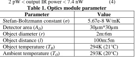
(Φ). This power will be incident on the bolometer detector. Therefore, this equation can model the behavior of the optics module. A verilog-A code is written to simulate equation (3) and construct the optics model that can be used as the first stage of the circuit. The optics model block, shown in Figure 1 can be reused in any other circuit as a sub-module. This is flexible for any other case parameters. Table 1 demonstrates the used parameters for the optics module. These parameters were proposed for a human or a vehicle targets that have diameter of 2m and 6m, respectively. These targets are supposed such that they are 5-100m apart from the IR camera and having a worst-case condition of 1°C temperature difference from ambient. The output power calculation, based on the above model, provides the following limits for the power incident on the detector pixel as the following equation.
2 pW < output IR power < 7.4 nW (4)
Table 1. Optics module parameter
Parameter Value
Stefan-Boltzmann constant (σ) 5.67e-8 W/mK Detector area (AD) 30µm*30µm
Object diameter (r) 2m:6m
Object distance (l) 100m:5m
Object temperature (TB) 294K (21°C)
Ambient temperature (TO) 293K (20°C)
The second module of the IR camera is the detector array, namely the resistive bolometers. The active material resistance of the bolometer changes with the IR radiation power according to its temperature coefficient of resistance
(TCR), so this feature is used to detect the change in the IR radiation. The main function of the bolometer is to transform the change in the incident IR radiation power to a change in its resistance. The resistance of the bolometer depends on the material type, dimensions, and incident IR radiation. The bolometer resistance as a function of incident IR radiation is given in [2, 5, 17] by:
(5)
where, RO is the dark resistance of the bolometer without
incident IR radiation, α is the TCR, η is the IR absorbance, Φ is the IR radiation power, Gth is the thermal conductance, Cth
is the thermal capacitance and ω is the chopping frequency. Equation (5) demonstrates the bolometer resistance as a function of IR radiation power and the bolometer parameters. Based on equation (5) and using verilog-A code, the bolometer model can be constructed.
The input of the model is the IR radiation power output of the optics model and its output is the new resistance value of the bolometer. Note that the only input to the model is the IR radiation power, as it is varying with the temperature of the object. The rest parameters are constant since they are material dependent. This model was applied to the vanadium oxide (VOX) bolometer as it is the most popular bolometer used in high performance imagers [18]. Table 2 lists the VOX material parameters.
Table 2. Bolometer material properties
Parameter value unit
Cold bolometer resistance (RO) 100 kΩ
TCR (α) − 2% / K
IR absorbance (η) 90%
Thermal conductance (Gth) 0.5×e −7 W/K
Thermal capacitance (Cth) 0.5×e − 9 J/K
Chopping frequency (ω) 2π×10 rad/s The 100k resistor (Rcold as in Figure 1) is connected in series
with the bolometer to simulate the blind bolometer to suppress the dark current effect. In Figure 1, the voltage supply is 1.2 V and the nominal current flowing in the bolometer branch with no radiation is 6μA. The bolometer resistance is decreased when the IR radiation incident on the optics for simulated extreme output in the range of 2pW to 7.4nW. The extreme values of the current flowing in the bolometer branch will change from 1.8pA to 6.7nA above the nominal 6μA. The current change (Iout) due to the IR radiation power extremes is
a very low varying current in the range of 1.8pA < Iout <
6.7nA. For the worst-case condition, compensating for medium and optics loses; a higher range of current swing will be selected for the CTIA design. The input current values are selected in the range of 1pA < Iout < 10nA.
2.2 Circuit Topology
Figure 1 illustrates the schematic diagram of a conventional CTIA circuit. It consists of three main parts which are the op-amp, the integration capacitor Cint, and the reset switch. The
behavior of the op-amp affects the overall performance of the CTIA. There are two modes of the CTIA operation: the reset mode and the integration mode. During the reset mode, the Cint is reset to a reference voltage shown in Figure 1, by
Fig. 1: Schematic diagram of the CTIA ROIC
2.3
Design of the op-amp
Figure 2 illustrates the schematic diagram of a classical two-stage op-amp and its biasing circuit. The first two-stage is the classical differential amplifier that consists of two PMOS transistors as input devices M1 and M2 whose trans-conductance is gm1. These transistors are connected to a
current mirror load NMOS transistors M3 and M4. The second stage is a common source amplifier which consists of two transistors M6 and M7 to act as an output stage that controls the output swing and DC voltage level. The Miller capacitor CC and the transistor M9 are connected as the
feedback loop to establish the desired stability and the bandwidth of the op-amp. The biasing circuit is a Beta-multiplier reference that consists of NMOS transistors M11 and M22 and POMS transistors M33 and M44 [19]. The resistor R controls the reference current that will flow in the whole circuit. This reference circuit biases the two stages of the op-amp with almost constant current even if the voltage supply deviates from its original value (1.2 volts). The Beta-multiplier circuit needs a start-up circuit to ensure that it correctly works and the current flows through the two branches of the two-stage op-amp. The start-up circuit shown in Figure 2 consists of transistors M21, M23 and M24 [2, 19].
The two-stage op-amp offers high gain, low-noise, and the highest output signal swing while dissipating medium power if compared to other op-amp topologies [2]. Therefore, it is the optimum topology for low-noise amplifiers used in IR ROICs. In addition, for battery-operated portable IR cameras and small signal amplitudes which can be easily affected by noise, a low-power and low-noise technique for designing two-stage op-amp will be discussed. The weak inversion technique will be applied in the presented op-amp design to minimize the power consumption. The dominant noise of the two-stage op-amp is the flicker noise and the thermal noise which are respectively given in [19, 20] by:
(6)
(7)
where, Vf_eq is the equivalent flicker noise voltage. Vt_eq is the
equivalent thermal noise voltage. KAP and KAN are the flicker
noise coefficients for the PMOS and NMOS transistors, respectively. KPP and KPN are the thermal noise coefficients
for the PMOS and NMOS transistors, respectively. Based on equation (6) and equation (7), there are three design keys that can be used to reduce the flicker and thermal noises [20]:
1)Using PMOS transistors as input pairs M1 and M2.
2)Ensuring that W1,2 >> W3,4.
3)Ensuring that L1,2 << L3,4.
where, W1,2 and W3,4 are the channel widths of the input and
load transistors, respectively and L1,2 and L3,4 are the channel
lengths of the input and load transistors, respectively.
The Beta-multiplier biasing circuit is specifically designed for generating a reference current with minimum sensitivity to the variation of VDD. The resistor R is inserted into this circuit to
control the reference current.
The main objective of the presented op-amp design is to achieve low-power and low-noise performance. Therefore, the device sizes and biasing conditions will be designed using the following steps.
Step 1: The desired phase margin will be used for the selection of the minimum value for the compensation capacitor CC in Figure 2. For a 60° phase margin, the
following relationship will be used [20]: CC = 0.22 CL. If the
load capacitor (CL) is 5pF, the compensation capacitor CC will
be 1.1pF
Step 2: Choosing the total bias current of the two-stage op-amp (Ibias) according to the required power consumption: Ibias=
Pdiss / VDD. The target power dissipation is less than 3μW and
the VDD is 1.2V then, the Ibias will be 2.5μA. This current
Fig. 2: Schematic diagram of the two-stage op-amp with the beta-multiplier biasing circuit.
Step 3: Determining the first stage bias current from the slew rate (SR) requirement [20]: ID5 = SR x CC. The SR is required
to be 1V/μs and the CC is calculated as 1.1pF. Then, the bias
current of the 1st stage (ID5) will be 1.1μA. The current that
flows in each branch of the first stage of the differential amplifier will be: ID1 = ID2 = 0.5 x ID5 = 0.55μA. The
trans-conductance of the input transistors can be calculated as [19, 20]:
(8) Hence, the bias current of the second stage is given by: ID7 =
Ibias - ID5 = 1.4μA. (In addition, gm1,2= gm3,4.)
Step 4: Setting the gate-source voltage VGS of the transistors
operating in sub-threshold region. From the equation [19, 20],
(9)
The threshold voltage Vt of the input pair transistors M1 and
M2 is a technology parameter and equals -0.4V. T is the absolute temperature, and n is the slope of the curve in the weak inversion region, and K is Boltzmann constant, and q is the electron/hole charge. Typically n is 1 < n < 3. VGS will be
less than -0.35V. Assume VGS will equal -0.25V.
Step 5: Determining the aspect ratios of transistors M1, M2, M3, M4 and M5 such that they operate in the sub-threshold region based on equation (10) and equation (11) [19, 20].
(10) and
(11)
where, IS is the characteristic current or the drain current when
VGS =Vt, The aspect ratios of these transistors are tabulated in
Table 3.
Step 6: Determining the aspect ratios of transistors M6 and M7. For the 60° phase margin, the location of output pole is assumed to be placed at 2.2 times unity gain bandwidth, so the trans-conductance gm6 can be given by [19, 20]:
(12)
(13)
(14)
where, S = W/L. Also, increasing gm6 will improve the stability
of the op-amp. This is called pole splitting [21].
Step 7: Right half plane (RHP) zero compensation of the op-amp: the RHP zero introduces negative phase shift or phase lag in the transfer function of the op-amp which makes the stability be more difficult, so connecting a resistor (RZ) in the
feedback series with the compensation capacitor CC will be a
suitable solution. The RHP zero for the two-stage op-amp is given by [21]:
(15)
From equation (15), the value of RZ will control the RHP zero
and equal 1/gm6 to eliminate it. Now, the resistance RZ will be
replaced by a transistor M9 so the aspect ratio (S9) of
transistor M9 can be determined by [21]:
(16)
(17)
where, Veff is the effective voltage of a transistor that equals
VGS - Vt.
The op-amp is designed in 1V 1 poly 6 metal (1P6M) Taiwan Semi-conductor Manufacturing Company Limited (TSMC) standard 0.13μm CMOS process transistor models, simulated using CADENCE® Spectre Electronic Design Automation (EDA) tool, and making use of Berkeley Short-Channel IGFET Version 3 (BSIM3v3.3) transistor models. Employing the above equations and design procedures, and then using some iterations on the virtuoso® tool, the proposed op-amp has been designed with aspect ratios as shown in Table 3.
The simulation results of the designed op-amp are compared to similar designs, published in [5-8]. These publications applied the two-stage op-amp as a core of the CTIA. These comparisons are summarized in Table 4. Note that the simulation results tabulated are from the post-layout simulations.
Table 3. Design aspect ratios of the op-amp.
Device Type No. of fingers
Finger width (μm)
L (μm)
M1,M2 P 10 10 0.26
M3,M4 N 2 5 16.5
M5 P 1 5 0.26
M6 N 1 10 0.24
M7 P 4 10 0.30
M9 N 1 0.22 10
M11 N 2 10 2
M22 N 6 10 2
M33,M44 P 2 10 2
M21 P 1 0.26 20
M23 N 5 10 0.26
M24 N 1 0.26 20
From Table 4, the voltage supply, used in these publications, varies from ±1.5V to ±7.5V, were operated in the strong inversion region. This is why the power consumption is high. To minimize the power consumption, the sub-threshold operation of transistors with a voltage supply of 1.2V was used in this work. Although this work reaches the lower power consumption, the DC gain and phase margins were comparable. As the input signal of the op-amp has a low frequency (chopping frequency around 10Hz), the high bandwidth and the unity gain-bandwidth product (GBW) is not critical values. The input referred noise was 53.2nV/√Hz which was the minimum of the available values. Finally, the DC offset voltage was 1.7mV which was the best of all except the results in [8].
Table 4. Simulation results of the op-amp and comparisons.
Parameter [5] [6] [7] [8] This work
Supply voltage (V) +5 +5 ±1.5 ±7.5 +1.2
DC Power Consumption(W) NA 0.28m 1.43m 95.9μ 2.95μ
DC open loop gain(dB) 75.75 NA 74 64.4 73.7
Total input referred noise @ 1kHz (nV/√Hz) NA Output: 11µ@ 1MHz 95 NA 53.2
Phase margin (deg) NA NA 62° 13.4° 61.1°
Unity gain band width (Hz) NA NA 1M 42M 803.2 k
F3dB frequency (Hz) 5 M NA NA 47k 262
CMRR (dB) 108.9 NA NA NA 80.6
Input Offset voltage (V) 26m NA 2.52m 116 μ 1.7m
To simulate the Beta-multiplier voltage reference, the DC analysis is used to sweep the voltage supply from zero to 2V and monitoring the output current that flowing in M22 device. The designed Beta-multiplier voltage reference achieves 28.5nA/Volt reference current variations with the voltage supply VDD changes. Therefore, if the voltage supply changed
±10% i.e. 0.12V the biasing current will change 3.42nA. This value represents 1.7% of the total biasing current (191.5nA). The rate of the current reference change with the voltage supply variation is a comparable value to 25nA/Volt which published in [22].
2.4
Design of the Integration Capacitor
In the ROIC array, the rows are sequentially activated. The row activation time is composed of two time intervals which are the integration time and the readout time. During one row activation, the current signal of each column is transferred to the CTIA circuit for conversion to voltage signal during integration time. After the integration time, the generated voltage from the CTIA of each column is sampled at a time, and its sample is serially transferred to the output stage during the readout time. The frame rate of the IR cameras is in the range of 30:60 frame/s. Hence, the frame time is 33.33ms (assuming frame rate is 30 frame/s). Assuming 320x240 array, the row select time becomes 104μs. Assuming the integration time and readout time are equal, the integration time is assumed to be 50μs. The column readout rate will be about 4.8MHz.
The output voltage of the CTIA can be determined from equation (18) [23].
(18)
where, Cint is the integration capacitor, iin is the input current
and tint is the integration time. The integration capacitor
should be small to save chip area and cost but this small value can cause saturation of the output voltage. Therefore, the
integration capacitor value should be selected as minimum as possible such that this value prevents saturation of the output voltage if the input current is maximum as calculated before (10nA). The minimum value of the integration capacitor enables the CTIA to integrate the minimum input current (1pA) and produces the output voltage above the noise levels. The problems of the noise and the output voltage saturation will be solved next section (section 3) by applying a noise reduction technique. If the input signal current is out of the expected input current range, another technique for widening the dynamic range (DR) will be discussed is section 4.
The value of the Cint is scanned from 400fF to 1.2pF with
maximum input current of 10nA and integration time of 50μs. It is found that the optimum value of the Cint to satisfy the
above rules is 800fF, as can be deduced from Figure 3. This is the value at which the maximum output voltage can be achieved without saturation.
Fig. 3: Integration capacitor selection.
2.5
Reset Switch Design
the selection of the reset switch dimensions is directly affecting the noise performance. To decrease this noise, the reset switch is typically made as small in width as possible to minimize the clock feed-through and charge injection that creates a voltage pedestal when the reset switch is opened. On the other hand, the reset switch length should be increased over the minimum value to avoid leakage through the switch [21, 24].
Fig. 4: CTIA output without connecting the dummy switch
Fig. 5: CTIA output with connecting the dummy switch based on the minimum input current
The reset transistor switch is connected to a dummy switch to minimize the clock feed-through and charge injection as shown in Figure 1. This dummy switch is controlled by a clock that is complementary to the clock that controls the reset switch and delayed by 300ns to minimize transient glitches. The input current was set to the minimum input value of 1pA. The output signal is supposed to start from the 600mV DC level and increase till the end of the integration time then it will be reset to 600mV. But, without connecting the dummy switch, it starts and ends below the 600mV DC level, shown in Figure 4. This is due to the effect of the clock feed-through which seems like the DC offset. The output signal with connecting the dummy switch is shifted up and the output signal becomes higher than the 600mV DC level at the end of integration time based on the minimum input current (1pA), shown in Figure 5. At this situation, the S/H circuit can capture the output signal of the CTIA circuit.
2.6
Sample and Hold Circuit Design
The CTIA output voltage expresses the input current value of the bolometer at each integration time. At each integration time, it is required to snapshoot the output voltage and store this value in a capacitor to generate the staircase input voltage to the analogue to digital converter (ADC) circuits. The sample and hold (S/H) circuit simply consists of a switch and
a capacitor, shown in Figure 1. The switching time is adjusted to take one sample at the end of the integration time and hold this sample value to the next sample to produce the staircase output voltage. To minimize the charge injection and clock feed-through effects of the switch, it is designed by a transmission gate. The transmission gate needs a synchronized complementary of the control signal. In Figure 1, the S/H transmission gate is switching according to the control signals SH and the complementary control signal SHB. Control signal SH has a pulse width of 10μs and start at time 35μs from the beginning of integration time and ends at time 45μs from the beginning of integration time with the same frequency of resetting the Cint. This timing enables capturing at least one
sample at each integration time.
2.7
Transient Analysis of the CTIA
The transient analysis was run on the CTIA circuit shown in Figure 1. The Cint is connected in the feedback loop of the
op-amp and the reset switch with the dummy switch is connected parallel to the Cint. The input current is adjusted to the range
of 1pA:10nA as discussed before. The control signals of the reset switch and the S/H switch are shown in Figure 6. Figure 6a illustrates the integration capacitor reset signal which controls the integration time. Figure 6b illustrates the control signal of the S/H circuit.
Figure 7 shows the transient response of the CTIA and S/H circuits with DC input current 5nA and Figure 8 illustrates the transient response of the CTIA and S/H circuits when the input current is sinusoidal signal with frequency 1 kHz and amplitude of 5nA. The upper curves in Figure 7 and Figure8, named Vo1 are the output signals from the CTIA circuit. The
lower curves in Figure 7 and Figure 8, named Vo2 are the
staircase output signals after the S/H circuit. The sample is captured 5μs before the end of integration time with pulse width 10μs. As mentioned before, the CTIA is simply an integrator. The integration process is illustrated in Figure 7 and Figure 8. As the input current has a constant value with time, the output voltage is a linear function of time. The slope of the output voltage depends on the input current value and the value of the Cint. The application of the sinusoidal wave
input signal is performed in order to test the behaviour of the CTIA circuit with variable amplitude signal as shown in Figure 8. Note that the CTIA and the S/H outputs start from the 600mV (half rail). In Figure 9, the input current is scanned from 1pA to 10nA with the same value of the Cint and the
integration time. Notice that for this range of input current, the output voltage doesn’t saturate.
Fig. 7: Transient response with DC input current
Fig. 8: Transient response with sinusoidal input current
Fig. 9: Output voltage from scanning input current
3.
CTIA WITH CDS TECHNIQUES
The CDS technique is a sampling technique that is used to eliminate the detector node noise and the DC offset voltage at the input of the interface circuit. The CTIA converts the input current from the bolometer to the output voltage that will be sampled and held in an S/H capacitor (CS/H) by the S/H
circuit. Figure 10 illustrates the circuit diagram of the CTIA with application of the CDS technique. There are two modes of operation, the reset mode and the integration mode. In the reset mode, the switches ‘rst’ are switched on and switch ‘int’ is switched off. The voltage of the node A is VREF ( = 0.6 V),
and the voltage of node B is VREF + VOS. VOS is the offset
voltage of the op-amp. Then, the stored voltage in the offset storage capacitor, COFF, becomes -VOS.
Fig. 10: Circuit diagram of the CTIA with the application of the CDS technique
During the integration mode, the switch ‘rst’ are switched off and the switch ‘int’ is switched on. The signal integration and accumulation occurs in the integration capacitor Cint. The
offset voltage, VOS, is cancelled-out in the integrator output as
it is stored in the COFF. At the end of the integration time, the
‘sample’ switch is switched on to sample the output voltage of the circuit and hold it on the CS/H. Figure 11 shows the control
signals of switches ‘rst’, ‘int’ and ‘sample’. Note that these signals are non-overlapping clocks and the switches are active low since it is implemented as PMOS transistors.
Figure 12 shows the complete schematic diagram of the CTIA with CDS integrated with optics and bolometer models as drawn in virtuoso® tool. The dummy switch is connected in series with each switch to minimize the effect of charge injection. This switch is controlled by the complementary clock of its corresponding switch. There is a small time shift between switch clocks and dummy switch clocks to ensure that the canceling charge of dummy switch cannot escape through original switch. The bolometer model was connected in series with another constant resistance to model the effect of the cold bolometer that suppresses the dark current. The proposed CTIA with CDS was designed with aspect ratios as shown in Table 6.
Table 5 summarizes the effect of the application of the CDS technique on the CTIA. The closed loop gain is reduced to 28.6 dB due to adding the COFF, but the offset voltage is
Table 5. Simulation results of the CTIA with CDS
Parameter CTIA
Without CDS
CTIA With CDS
Technology (nm) 130 130
Supply voltage (V) 1.2 1.2
Power Cons./pixel (μW) 3.3 3.3
Bandwidth (KHz) 3 19.3
Closed loop gain (dB) 42.4 28.6
GBW (kHz) 395.6 459.1
Phase margin 63.2° 82°
RMS Input noise (pA) 60 6.1
Offset voltage (μV) 18 10
Table 6. Design aspect ratios of the CTIA with CDS
Device Position Type Aspect ratio W/L
M1 rst (left) P 150n/6u M2 rstb (left) P 150n/130n
M3 int P 150n/130n
M4 intb P 150n/130n
M5 rst (middel) P 150n/130n M6 rstb (middel) P 500n/1.1u
M7 rst (up) P 150n/6u
M8 rstb (up) P 500n/1u
M9 sample P 150n/130n
M10 sampleb N 150n/130n
Fig. 11: Control signals of the CTIA with CDS
4.
POST-LAYOUT SIMULATION OF
THE CTIA WITH CDS
The CTIA with CDS circuit is designed and implemented in standard TSMC 0.13 μm CMOS process with BSIM3V3 device model. The design rule check (DRC), layout versus schematic (LVS), parasitic extraction (PE), process-voltage-temperature (PVT) analysis and post-layout simulation are performed for all designed circuits. Spectre simulator is used to perform the post-layout simulation in CADENCE® software. Figure 13 shows the complete layout of the CTIA with CDS circuit. The total chip area is 70μm×108μm.
Table 7 summarizes the effect of application of the CDS technique based on the post-layout simulation. Note the RMS input noise is reduced from 31.5pA to 4.9pA and the offset voltage is reduced from 772μV to 145μV for the same power consumption of 6.5μW (5.2μW excluded the bias circuit).
Table 7. Post-layout simulations of the CDS effect
Parameter Without CDS With CDS
Technology (nm) 130 130
Supply voltage (V) 1.2 1.2
Power Cons./pixel (μW) 6.5 6.5
Dynamic range (dB) 110.4 98.7
Closed loop gain (dB) 49.6 28.2
GBW (KHz) 291.3 284.2
Phase margine 51° 56°
RMS Input noise (pA) 31.5 4.9
Offset voltage (μV) 772 145
Fig. 13: Compelete layout of the CTIA with CDS circuit
Table 8 compares the specification of the CTIA with CDS to published works. Note that the values of the specifications of
this work are based on the post-layout simulations. The proposed CTIA with CDS circuit consumes the minimum-power consumption of all published works except of the power consumption that is reported in [10]. In paper [10], the core of the CTIA is a common source transistor used as the amplifier. This common source amplifier uses only one transistor to amplify the signal and another transistor works as a load. This configuration explains why that design has the minimum power consumption per pixel however; the total power consumption is not the minimum because this design has other peripheral circuits like current skimming and output buffer. The output noise of the presented work is the minimum value of all compared published works.
The dynamic range of the proposed circuit is 98.7dB according to Table 8, and will be 114dB (if the analog divider uses a voltage supply 5V, will be discussed in section 4). The proposed circuits will be applied at the column level not at the pixel level. As a result, the high layout area is not a very critical problem. The other parameters of the readout circuit like readout rate, input current range, integration time and integration capacitor are comparable values to published works.
All above simulations are rerun under the effect of the process-voltage-temperature (PVT) variations. The PVT analysis is applied on the layout ofthe CTIA with CDS. This analysis is run to check the operation of the circuit under these variations. The cadence® tool offer five models of MOS devices which are typical, fast N fast P, fast N slow P, slow N fast P and slow N slow P. These models are used to simulate the process variations. The voltage supply is assumed to change ±10% of 1.2 V so, the voltage supply variations is from 1.08V to 1.32V. Finally, the temperature variations is assumed to be from -55°C to 125°C as this range of temperature concerns with military applications. Table 9 summarizes all specifications of the layout of the CTIA with CDS circuit under the PVT variations.
The maximum power consumption is due to the 125°C corner. However, the AC response of that temperature is superior; the circuit has the maximum GBW and the largest phase margin. In contrast, the -55°C corner has the minimum power consumption but it has the maximum bandwidth and the circuit is still stable. As the voltage supply changes from 1.08V to 1.32V, the power consumption increases by 20% while the RMS input noise and offset decreases by 4% and 1.3%, respectively. The DC gain decreases by 1.4% while the GBW and bandwidth increases by 2.2%. Although the power consumption is increased by 20%, this value does not exceed the corresponding compared value of power consumption. The power consumption is directly affected by the change in the voltage supply and this is normal since the power consumption is directly calculated from the voltage supply value. The biasing circuit (beta-multiplier voltage reference) of the op-amp decreases the effect of the voltage supply change on the total specifications.
Table 8. Comparisons of the CTIA with CDS specifications
Parameters [10] [18] [11] [9] [6] This work
Technology (nm) 350 500 500 180 600 130
Supply voltage (V) 5 5 5 3.3 5 1.2
Power Cons./pixel (μW) 2 N.A. 40 25.5 280 6.5 Total power (mW) 8.94 175 N.A N.A. N.A. 1.56 RMS output noise (μV) N.A. 534 260 240 11 6.9
DR (dB) N.A. N.A. 102 138 64.9 98.7
Readout rate (MHz) 3 8.3 N.A. 1 5 4.6
I/P current range (A) 1p:10n N.A. N.A. <200n N.A. 1p:10n
Cint (F) 240f 3:10p N.A 100f N.A. 800f
Tint (μs) 10 20:80 N.A 1000 N.A. 50
Pixel pitch (m2) 30μ 35μ N.A 30μ× 15μ N.A. 70μ× 108μ
Table 9. PVT analysis summary of the layout of the CTIA with CDS
Parameter NOM Process VDD ± 10% Temp.
SS FF SF FS 1.08V 1.32V -55 °C 125 °C
Power Cons./pixel (μ W) 6.5 4.58 9.21 8.91 4.7 5.28 7.85 3.6 12.48
RMS input noise (pA) 4.9 4.2 5.6 5.3 4.4 5.1 4.7 4.4 5.5
Dynamic range (dB) 98.7 97.9 99.5 99.4 98.2 98.9 98.6 101.2 96.5
Offset voltage (μV) 145 879 340 7 183 135 143 12 494
DC gain (dB) 28.2 24.2 31.1 29.9 24.8 28.7 27.6 25.1 30.3
F 3dB (kHz) 17.3 20.9 15.8 17.4 20.4 15.9 19.1 21.2 16.9
GBW (kHz) 284.2 214.5 357.1 355.7 220.7 276.6 290.7 229.6 366.4
PM (Deg) 56 54 59 64 49 57 55 51 63
5.
NEW WDR TECHNIQUE OF THE
CTIA WITH CDS
5.1
Basic Idea
Figure 14 illustrates the basic idea of a new proposed technique for widening the dynamic range (WDR). The y-axis of Figure 14 represents the output voltage of the CTIA with CDS circuit before the S/H circuit and the x-axis is the time. The output voltage starts from DC voltage of 600mV (half rail). When the input current is in the normal range, the output voltage does not exceed the saturation voltage (VREF2=1.2-3VT
according to the weak inversion technique [19, 20]) before the end of the integration time t2. However, if the input current is
greater than 10nA, the output voltage will saturates to volt V1
(V(t1)) at time t1. At time t2, the output voltage is supposed to
reach the voltage V2. From the two triangles (ABE), (ACD) in
Figure 14, it can be deduced that
(19)
V1 is the saturation voltage which equals VREF2, t2 is the
integration time which equals 50μs and t1 is the time at which
the saturation takes place. The periodic ramp signal with amplitude of 1.2V and time period of 50μs, shown in Figure 18, is used to substitute the ratio of t2/t1 in equation
(19). The slope (S) of the ramp signal in Figure 15 is 1.2V/50μs. The time can be converted to voltage by multiplying it by the ramp signal slope S:
(20)
The voltage corresponds to the time of saturation t1 will be:
(21)
Substituting V1 by VREF2, t2 by 50μs and t1 by the value
obtained from equation (21). Hence, equation (19) can be rewritten as
(22)
where, Vbias = 1.2 × VREF2= 1.2 × (1.2-3VT), VT = KT/q.
Fig. 14: Basic Idea of the WDR Technique
Fig. 15: The ramp signal
It is clear from equation (22) that the core of the WDR topology is the analogue divider between the constant value Vbias and the value of V1. Figure 16 illustrates the block
diagram of the new WDR technique, and Figure 17 illustrates the circuit diagram for the WDR technique applied to the CTIA with CDS.
The comparator compares this value to the VREF2. At the
moment that Vo1 exceeds VREF2, the comparator generates
output signal (Vcomp). This signal is fed to the edge detector
that triggers the normally opened NMOS device switch (S2).
When this switch is turned on, the output of the ramp generator will be connected to the analogue divider. It divides the constant bias voltage (Vbias) to the voltage of the ramp
signal V1 at the time of saturation (t1). At this moment, the
output of the divider represents the estimated output voltage (V2). Figure 17 shows the full circuit diagram of the WDR
technique applied on the CTIA with CDS.
Fig. 16: Block diagram of the new WDR technique
5.2
Simulation results
The main components of the WDR are realized using AHDL models to approve the idea of this technique. Figure 18 shows the output waveform in the case of the sinusoidal input current wave. At the integration time 50μs and 450μs of Figure 18, the CTIA output signal doesn’t exceed the reference voltage of the comparator and the circuit operates normally. At the integration time 150μs, 250μs and 350μs of Figure 18, the CTIA output signal exceeded the reference voltage of the comparator. The WDR circuit operates and the estimated output voltage is connected to the S/H circuit instead of the CTIA output. The dynamic range of this technique depends on the voltage supply of the analogue divider that produces the estimated output voltage. Therefore, if the analogue divider supply voltage is 5V, the dynamic range will increase from 98.7dB to 114dB as the maximum allowed output voltage increased from 0.6V to 4.4V (the DC level of the signal is 0.6V).
Fig. 17: Circuit diagram of the WDR technique applied on the CTIA with CDS
6.
CONCLUSION
In this paper, the design of a column level IR ROIC circuit is presented. The optics and bolometer detector were modeled using AHDL to simulate the input signal to the IR ROIC. The CTIA ROIC targets the minimum power consumption along with minimum noise so all transistors are biased to operate in the sub-threshold region. The power consumption of this circuit including the biasing circuit was 6.5μW (5.2μW excluded the bias circuit) with the RMS input noise of 31.5pA while the integration capacitor was 800fF. The CDS technique is applied to the CTIA circuit to minimize the noise and offset effects. The RMS input noise was reduced to 4.9pA, and the offset voltage was reduced to 145 μV while the power consumption remains 6.5μW.
The presented designs are implemented in 0.13µm, 1V 1P6M TSMC standard CMOS technology. Cadence Spectre EDA tool, making use of BSIM3v3.3 transistors models, is used for different simulations. All these circuits were subjected to layout, DRC, LVS, PE, and post-layout simulations as typical IC design flow. The overall area of the CTIA with CDS circuit was 70μm*108μm. The PVT variation analysis studied all circuit specifications under the variation of process, voltage, and temperature corners. The PVT analysis results predict some change of the circuit specifications. However, these changes are still comparable to the nominal (typical) values, and having better results compared to the published works.
Finally, the new technique for the WDR was applied to the CTIA with CDS to improve its DR of the presented low-power low-noise ROIC. The WDR technique components were implemented by a behavioral AHDL models to verify the idea of widening the DR. The transient analysis was run on this technique and showed the successful operation. The DR was increased since it is voltage supply dependent. This technique will operate only if the CTIA output reaches the saturation.
7.
REFERENCES
[1] C.-C. Hsieh, C.-Y. Wu, F.-W. Jih, and T.-P. Sun, "Focal-Plane-Arrays and CMOS ReadoutTechniques of Infrared Imaging Systems," IEEE Transactions on Citcuits and Systems for Video Technology, vol. 7, NO. 4, pp. 594-605, Aug. 1997.
[2] M. Rafat, “CMOS Readout Integrated Circuit Design for Infrared Imagers,” M.Sc. thesis, Military Technical College, Egypt, 2015.
[3] J. F. Johnson and T. S. Lomheim, "Focal-plane signal and noise model–CTIA ROIC," IEEE Transactions on Electron Devices, vol. 56, pp. 2506-2515, Nov. 2009.
[4] A. Ruan, K. Shen, and B. Hu, "Adjustable gain CTIA cell with variable integration time for IRFPA applications," International Conference on Communications, Circuits and Systems (ICCCAS 2009), pp. 1066-1069, July 2009.
[5] F. K. Saleh, "The design and integration of CMOS readout circuitry with an a GexSi1-xOy Cooled Micro-bolometer," master, electronic engineering, carleton, ottawa,ontario,canada, 2007.
[6] Z. Zhu, Y. Yang, and Q. Meng, "A low noise Si-CMOS amplifier-multiplexer readout circuit array for imaging applications," 8th International Conference on
Solid-State and Integrated Circuit Technology, ICSICT'06, pp. 629-633, Oct. 2006.
[7] Y. Ha, M. Li, and A. Q. Liu, "A New CMOS Buffer amplifier design used in low voltage MEMS interface circuits," Analog Integrated Circuits and signal processing, vol. 27, pp. 7-17, April 2001.
[8] G. R. Cugler Fiorante, P. Zarkesh-Ha, J. Ghasemi, and S. Krishna, "Spatio-temporal tunable pixels for multi-spectral infrared imagers," in IEEE 56th International Midwest Symposium on Circuits and Systems (MWSCAS 2013), pp. 317-320, Aug. 2013.
[9] S. Kavusi, K. Ghosh, and A. El Gamal, "Architectures for high dynamic range, high speed image sensor readout circuits" Springer, Nov. 2006.
[10] y.-c. l. tai-Ping Sun, hsiu-li shieh, "A novel readout integrated circuit with a dual-mode design for single- and dual-band infrared focal plane array," el sevier ,infrared physics and technology, March 2013.
[11] J. Lv, Y. Jiang, D. Zhang, and Y. Zhou, "Ultra-low-noise readout integrated circuit for uncooled microbolometers," Electronics letters, vol. 44, pp. June 2008.
[12] S. Kavusi, K. Ghosh, K. Fife, and A. El Gamal, "A 0.18 μm CMOS 1000 frames/sec, 138dB Dynamic Range Readout Circuit for 3D-IC IR Focal Plane Arrays," IEEE Custom Integrated Circuits Conference, (CICC'06), pp. 229-232, Sept 2006.
[13] C.-C. Hsieh, C.-Y. Wu, F.-W. Jih, T.-P. Sun, and H. Chang, "A new CMOS readout circuit design for the IR FPA with adaptive gain control and current-mode background suppression," IEEE International Symposium on Circuits and Systems, (ISCAS'96), pp. 137-140, May 1996.
[14] C. C. Enz and G. C. Temes, "Circuit techniques for reducing the effects of op-amp imperfections: autozeroing, correlated double sampling, and chopper stabilization," Proceedings of the IEEE, vol. 84, pp. 1584-1614, Nov 1996.
[15] X. Li, S. Yao, and Y. Zhao, "CMOS readout circuit with new background suppression technique for room-temperature infrared FPA applications," Journal of Circuits, Systems and Signal Processing, vol. 29, NO. 6, pp. 1027-1040, Dec. 2010.
[16] B. Hu, P. Li, and A.-w. Ruan, "A Multifunction snapshot ROIC design for low and high background application," International Conference on Optoelectronics and Image Processing (ICOIP), pp. 44-46, Nov. 2010.
[17] P. L. Bin Hu, Ai-wu Ruan, Dao-ming Lin "Design and verification of 160*120 bolometer ROIC," International Conference on computional problem-solving (ICCP), Oct. 2011.
[18] J. Lv, H. Zhong, Y. Zhou, B. Liao, J. Wang, and Y. Jiang, "Model-Based Low-Noise Readout Integrated Circuit Design for Uncooled Microbolometers," IEEE SENSORS JOURNAL, vol. 13, pp. 1207-1215, April 2013.
simulation vol. 18: Wiley-IEEE Press, 2011.
[20] P. E. Allen and D. R. Holberg, CMOS Analog Circuit Design. vol. 7: Oxford University Press, 2002.
[21] D. A. Johns and K. Martin, Analog integrated circuit design: Wiley. com, 2008.
[22] T. Shima, "Temperature insensitive current reference circuit using standard CMOS devices," 50th Midwest
Symposium on Circuits and Systems, MWSCAS, pp. 181-184, 2007.
[23] J. Seo, G. Kim, K. Lim, C. Seok, H. Kim, S. Im, J.-H. Kim, C.-Y. Kim, and H. Ko, "An analog front-end IC with regulated RI amplifier and CDS CTIA for microbolometer," 13th International Conference on Control Automation and Systems (ICCAS 2013), pp. 1312-1315, Oct. 2013.