Modeling and Performance of TBSC
Compensator for Power Factor Correction with
Eliminating Harmonic Resonance in Growing
Industries
Prof. Dhanaji Patil Prof. Pradnya Patil
Department of Electrical Engineering Department of General Engineering Padmabhooshan Vasantraodada Institute of Technology,
(MS), India
Padmabhooshan Vasantraodada Institute of Technology, (MS), India
Abstract
An application of the capacitor for reactive power compensation but there are problem of harmonic resonance which becomes a very dangerous problem to reactive power compensation in power systems, paper presents reactive power compensation without creating harmonic resonance under variable load condition. The planned controller may be function as a retrofitting device to replace existing reactive power controllers with small variations. Topology for reactive power compensation suitable for dyna mic loads in closed loop system. The scheme consists of (TBSC) Thyristor Binary Switched Capacitor banks are used for reactive power compensation and avoiding harmonic resonance problem.
Keywor ds: Capacitor Switching, Variable Load, Reactive Power Compensation, TBSC, Harmonic Resonance
________________________________________________________________________________________________________
I. INTRO DUC TIO N
It is known that the power loss in distribution network systems on account of low power factor, because of insufficient react ive power compensation technique and their improper control technique. The capacitor can be switch directly connected to load for reactive power compensation which improves the operating condition. The shunt capacitor installations are in very big manner [1]. Because of the development of power distribution network with new connections to undeveloped area, increasing inductive loads resulted in low power factors. This is giving rise to large losses and billing charge in the power distribution network.
An application of reactive power compensation has highly importance on growing industrial sector to improve power quality. Reactive power compensation is based on controller that can perform compensation without harmonic resonance under given load condition. The proposed controller will be implemented based on microcontroller to compensate reactive power without resonance. Most loads of the power system are inductive in nature and hence operate at a lagging reactive power to avoid this capacitors are installed in circuit for reactive power compensation. Reactive power compensation in commercial utilities connect capacitor bank across with the load [2]. But one of the major problems is the so -called ‘harmonic resonance’, which cause amplification of current and voltage harmonics. This happening is caused by parallel and series resonance at harmonic frequency between capacitors and power system inductances. The objective of project is reactive power compensation with eliminating harmonic resonance. More recent works have focused on the mechanism of active and passive harmonic filters. This approach can be difficult and be costly to the customers. Reactor is connected series with capacitor for avoid the resonance problem but this installation is costly and complicated [3].
The operation of nonlinear loads in a power distribution system creates harmonic currents that flow throughout the power system. As the frequency increases or as the harmonic order increases, inductive reactance of power system increases with capacitive reactance decreases. The crossover point exists where the inductive and capacitive reactance is equal at given harmonic frequency. This crossover point called the parallel resonant point is where the power system has coincidental similarity of system imped ances. Every system with a capacitor has a parallel resonant point [4]. Harmonic resonance results in very high harmonic currents an d voltages at the resonant frequency. The scheme arranging the thyristor switched capacitor units in five binary sequential ste ps. This enables the reactive power variation with the least possible resolution. The proposed controller shifts the resonant point to another frequency when resonance conditions exist at that time capacitor bank should be changed in size.
II. DESIRABLE FEATURES
Possible solutions to avoid resonance:
1) Changing capacitor bank location and size; 2) Adding a reactor in series with capacitor bank;
From above methods these are used to the controlling the resonance effect. But the third method is essential and important fo r compensate the reactive power compensation as well as avoided harmonic resonance requirements under varying demand conditions. The installation of filters to limit harmonic can bring unwanted additional operational costs [5]. Basically, the idea is
to develop a controller that relies on common low cost sensing devices and does not require additional measurements. The desirable features of the proposed scheme are as follows:
It maintains the power factor at the PCC to any particular value. Capacitors are sized in binary sequential steps for minimum the step. It eliminates possible over compensation and resulting leading power factor. Avoid harmonic resonance problem.
The combination offers greater flexibility in control.
III. PRO PO SED TO PO LO GY DES C RIPTIO N
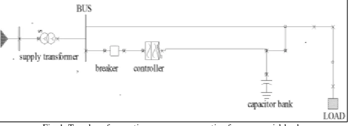
The proposed topology approach for reactive power compensa tion in power system consists of TBSC bank connected in parallel with the load at the PCC. As one can observe, control unit are used for capacitor bank are used for capacitor switching. Cont actor or breaker may cause transient at time of switching. To avoid this transient, thyrister is used in TBSC bank to make transient free switching which is operated in close loop control [6].
Fig. 1: Topology for reactive power compensation for commercial load.
Presence of harmonics increases interference in electronic systems, abnormal heating of cables and excessive capacitor currents flow. At resonance conditions, the capacitor bank can be changed in size to move the resonance point to another frequency or small reactors should be connected in series with the capacitors circuit as well as change the capacitor rating to avoid the resonance condition [5].
Fig. 2: Variation of reactive power with switched and fixed capacitors.
Fig. 2 Illustrates shows fixed capacitor banks provide for the fixed capacitor load conditions and Switched capacitor banks are designed for load levels above the minimum condition. i.e. for peak load period [7].
Required reactive power can be calculated by following formula.
(1)
kW is the system kilowatt load.
kvar is the amount of capacitive kilovar to be added.
)} tan(cos
) {tan(cos
*
var kW 1pfold 1pfnew
Fig. 3: Commonly method used for P.F correction through switched capacitor banks.
1) 1st read the voltage and current of the circuit, from that current and voltage calculate the P.F. 2) The calculated P.F is less than required pf then switch ON the capacitor.
The study of capacitor does not possible without harmonic discussion. The purpose of th is paper is to analyze, and talk about the issues and mitigation technique related to harmonic resonance. Due to the harmonic resonance in system it may cause damag e and dangerous to system equipment. i.e. Fuses will blow, circuit breakers will trip, or ca pacitors get heated up, reduce life and may fail. It can be avoid changing the resonant points i.e. maintaining desired power factor at PCC. Avoiding resonance is challe nging, but it’s possible [4].
Reactive power compensation in power system consists of connecting capacitor bank in across with the load. An application of capacitor bank, there is always risk of resonance. This is because of interaction between capacitor bank reactance and induct ive reactance of supply system. The harmonic current at near the resonance frequency can create high harmonic voltage across the capacitor bank and there is chance of burning or heating of capacitor [2].The reactance of a capacitor bank is inversely prop ortional to the frequency; therefore, this effect increases the dielectric stresses and heating. The result of increased voltage stress and heating decreases the life of capacitor [8]. The capacitive reactance and inductive reactance of power system are inversely to each o ther. There will be a point where the inductive reactance and capacitive reactance are equal. This condition may cause resonance in system. Consequently, the total impedance reaches to infinity and very high harmonic voltage may result if the facility harmo nic current has a frequency close to
= (2)
Where
,
1) MVAs is the system short-circuit level. 2) Mvarc is the capacitor size.
(3) Where, hr = Resonance frequency
hc= dominant harmonic frequency i.e.3,5,7,13……
Each capacitor it will deliver not less than rated reactive power and not more than 110% of rated reactive power at rated voltage and frequency. i.e. The capacitance of a unit will not vary more than –0% to +10% of the nominal value based on rated kvar, voltage and frequency [9].
To avoid harmonic filter are use but it can bring the unacceptable cost and complicated to reactive power compensation. We think that more suitable technique to control the capacitor switching for reactive power compensation and resonance of the consumers.
The parallel resonance order of 5.19 is close to the 5th harmonic order and if any magnitude of 5th harmonic current flows fr o m the harmonic-producing loads into the power system at the capacitor bus, the capacitor may not be able to withstand the resonance voltage, leading to fuse blowing or capacitor damage.
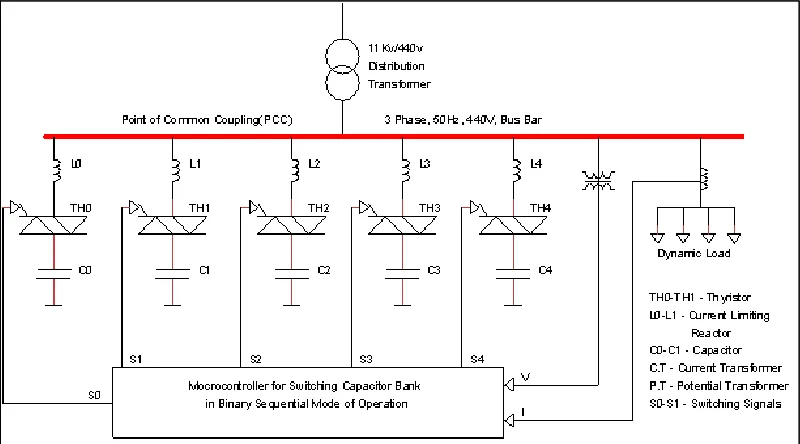
IV. CO NTRO LLER DESC RIPTIO N
A block diagram of reactive power compensator using TBSC (Thyristor Binary Switched Capacitor) banks is shown in Fig.4. Reference reactive power, QRef is calculated from the desired power factor. Actual reactive power at PCC, QActual is calculated by sensing voltage and current at PCC by P.T. and C.T. respectively. Error between QRef and Q Actual is given to PI Controller. A Discrete PI Controller is used. Output of PI Controller is given to ADC and its output is given to TBSC banks in such a way that no transients occur. In this way closed loop operation of TBSC banks for reactive power compensation is achieved [10]. The operating principle of each equipment as follows.
Fig. 4: TBSC Closed loop operation
TBSC consists of an anti-parallel connected thyristor and diode as a bidirectional switch in series with a capacitor and a current limiting small reactor. Transient free switching of capacitors is obtained by satisfying following two conditions:
1) Firing the thyristors at the negative/positive peak of supply voltage. 2) Precharging the Capacitors to the negative/positive peak of supply voltage.
In this case ensure that closing of the switch takes place at very nearer to zero voltage (zero voltage switching). This can be done more effectively with the help of thyristors as a controlled switches. A comparison of synchronized (thyristor) and non-synchronized (contactors) transients are dealt in the subsequent sections.
c M
MVAs
A. TBSC: (Thyristor Binary Switched Capacitor (TBSC):
The first condition satisfied accurately by timing the control circuitry and the second condition is only met immediately aft er switching off thyristor. The configuration for five capacitor bank steps in binary sequence weight with thyristors switch and inru sh current limiting reactors is shown in fig.5 [11]
TSC current is sinusoidal and free from harmonics, thus eliminating the need fo r any filters. Small series inductor is placed in series with capacitor. It serves following purposes.
It limits current transients during overvoltage conditions and when switching at incorrect instants or at the inappropriate v oltage polarity.
In the proposed paper TBSC bank step values are chosen in binary sequence weights to make the resolution small. If such ‘n’ capacitor steps are used then 2n different compensation levels can be provided.
B. Controller:
Controller is the heart of compensator. At PCC sen sed the voltage V and current I and Current Transformer (C.T.) by Potential Transformer (P.T.) respectively and given to controller. Controller determines the value of reactive power required to achiev e the desired power factor and then generates the control signals (gate signals) which are given to TBSC banks. By coordinating the control of TBSC, it is possible to obtain fully step less control of reactive power in closed loop. The control signals (gate signals) are given to TBSC banks.
V. SIMULATIO N RESULT
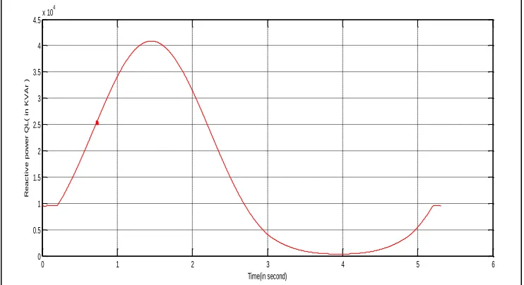
Continuously changing reactive power, QL is obtained by simulating three phase dynamic load. The nature of load variation is as shown in Fig.5. Minimum reactive power Qmin, maximu m reactive power Qmax, can be varied by changing the parameters of three phase dynamic load. In all simulations QRef is set to zero since it is assumed that desired P.F.is unity at all times
Fig. 6: Simulation result of three phase dynamic load
Table 1: Values of Five TBSC Bank
Sr. No. Q (in KVAR) C (in µF) L (in mH)
1 2.5 45 0.32
2. 5 90 0.16
3. 10 180 0.08
4. 20 360 0.04
5. 40 720 0.02
A. TBSC Closed Loop Operation
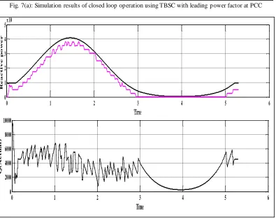
Discrete PI controller is used. 5 bit ADC is used in simulation. Parameters of Three -phase dynamic load block are adjusted in such a way that QL varies continuously from QMin. = 1 Kvar to QMax. = 75 Kvar. This variation takes place in five seconds. Waveforms of load reactive power QL, reactive power given by TBSC, Qcomp.(TBSC) and actual reactive power QActual at PCC are shown in Fig.6.From simulation results it is seen that Qcomp.(TBSC) closely follows QL with leading reactive power to avoid the resonance shown in Fig.7.(a), and with lagging reactive power to avoid the resonance shown in fig.7.(b). as follows.
0 1 2 3 4 5 6
0 0.5 1 1.5 2 2.5 3 3.5 4 4.5x 10
Fig. 7(a): Simulation results of closed loop operation using TBSC with leading power factor at PCC
Fig. 7(b): Simulation results of closed loop operation using TBSC with lagging power factor at PCC.
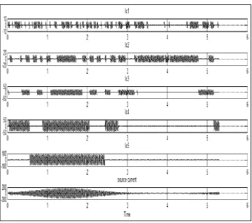
Current waveforms through all TBSC banks and source are shown in Fig.8 which are free from both harmonics and transients.
0 1 2 3 4 5 6
0 2 4 6x 10
4 Time R e c t i v e p o w e r
Q(Load) & QComp(TBSC)
0 1 2 3 4 5 6
-1 -0.5 0 0.5
1x 10
4 Time Q ( A c t u a l )
Q(Actual) at PCC
0 1 2 3 4 5 6
0 1 2 3 4 5x 10
4
Time
R e a c t i v e p o w e rQ(Load) & QComp(TBSC)
0 1 2 3 4 5 6
0 2000 4000 6000 8000 10000
Time
Q ( A c t u a l )Fig. 8: Current waveforms through all TBSC bank Source current.
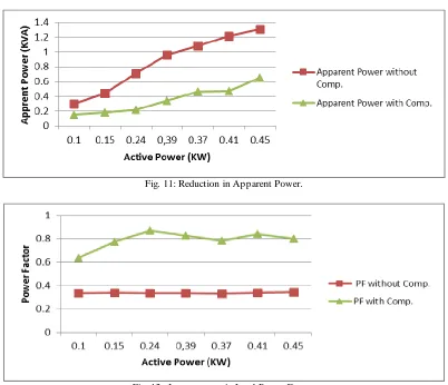
B. Comparison of Experimental Results
Fig. 9: Reduction in Load Current.
Fig. 11: Reduction in Apparent Power.
Fig. 12: Improvement in Load Power Factor.
An experimental setup is considered for the earlier selected six different loading conditions on the distribution transformer s. For the load increasing the actual power factor variation was observed to be 0.3 to 0.4 lagging corresponding to with the apparent power variation. The desired power factor at the point of common coupling has been set in the range. This is the narrow band considered for regulation purpose so as to maintain the resultant power factor nearer to unity always for the entire range of load variation.
VI. CO NC LUSIO N
The performance evaluation of Static Var Compensator consisting of capacitor bank in five binary sequential steps operated in conjunction with a TCR is carried out. A schematic diagram is given with a micro controller for switching and control operations; and a MATLAB program is presented with the sequential steps for the operations to be carried out. All the six cases are considered for performance evaluation and improvements brought out with compensator in receiving voltage. Current flowing through TBSC as well as source is transient free. Harmonic content in source current is negligibly small. By coordinating the control of T BSC, it is possible to obtain fully stepless control of reactive power. Also one can operate the system at any desired power factor. Proposed topology can compensate for rapid variation in reactive power on cycle to cycle basis. An attempt is made through this work t o develop a scheme with thyristors to reduce the cost by avoiding IGBT‘s and IGCT‘s, technically sound with reliable performance during both steady state and transient conditions, suitable for rapidly changing / fluctuating loads such as arc furnaces, tr actions loads, welding equipments etc., and self regulating operations are practically both transient and harmonics free. The scheme developed is most suitable for highly nonlinear, fluctuating and harmonic generating loads. It gives following benefits.
REFERENC ES
[1] “IEEE Recommended Practice for Electric Power Systems in Commercial Buildings”, ANSI/IEEE Std. 241 -1990, Gray Book. pp. 93 [2] R. C. Dugan, M. F. McGranaghan, and H.W. Beaty, “Electrical Power System Quality,” New York: McGraw-Hill, (1996), pp. 313,478.
[3] P. Jintakosonwit, S. Srianthumrong, and P. Jintakosonwit, “Implementation and performance of an anti-resonance hybrid delta-connected capacitor bank for power factor correction,” IEEE T rans. Power Del., Nov 2007, vol. 22, pp. 2543 –2551.
[4] J. Arrillaga and N. R. Watson, “Power System Harmonics”, 2nd ed. Hoboken, NJ: Wiley, 2003. pp. 142-150.
[6] U. Gudaru and D. R. Patil, “An Innovative Transient Free Adaptive SVC in Stepless Mode of Control”, World Academy of Science Engineering and T echnology 77, 2011, pp.200-207.
[7] IEEE Guide for “Application of Shunt Power Capacitors”, IEEE Std. 1036-1992, 1992, pp. 48,10.
[8] Boonseng, C. Chompoo-Inwai, V. Kinnares, K. Makawiwat and P. Apiratikul, “Failure analysis of dielectric of low voltage power capacitors due to re lated harmonic resonance effects,” in Proc. IEEE Power Eng. Soc. Winter Meeting, vol. 3, 2001, pp. 1003–1008.
[9] IEEE Standard for Shunt Power Capacitors, IEEE Std. 18 –2002, 2002.
[10] D. R. Patil, Member IAENG, U. Gudaru, Senior Member IEEE, “A Comprehensive Microcontroller for SVC wit Capacitor Bank in Binary Sequential Step Minimizing TCR Capacity”, 978-1-4244-1762-9/08/$25.00 c2008 IEEE.