This item was downloaded from IRIS Università di Bologna (
https://cris.unibo.it/
)
When citing, please refer to the published version.
This is the final peer-reviewed accepted manuscript of:
Said Hamdioui ; Hoang Anh Du Nguyen ; Mottaqiallah Taouil ; Abu Sebastian ; Manuel
Le Gallo ; Sandeep Pande ; Siebren Schaafsma ; Francky Catthoor ; Shidhartha Das ;
Fernando G. Redondo ; G. Karunaratne ; Abbas Rahimi ; Luca Benini, Applications of
Computation-In-Memory Architectures based on Memristive Devices, in 2019
Design, Automation & Test in Europe Conference & Exhibition (DATE), Proceedings
The final published version is available online at:
https://doi.org/10.23919/DATE.2019.8715020
Rights / License:
© 2019 IEEE. Personal use of this material is permitted. Permission from IEEE must be obtained for
all other uses, in any current or future media, including reprinting/republishing this material for
advertising or promotional purposes, creating new collective works, for resale or redistribution to
servers or lists, or reuse of any copyrighted component of this work in other works
Applications of Computation-In-Memory
Architectures based on Memristive Devices
Said Hamdioui1 Abu Sebastian2 Sandeep Pande3 Shidhartha Das4 G. Karunaratne5
Hoang Anh Du Nguyen1 Manuel Le Gallo2 Siebren Schaafsma3 Fernando G. Redondo4 Abbas Rahimi5
Mottaqiallah Taouil1 Francky Catthoor3∗ Luca Benini5
1
Computer Engineering, TU Delft, Delft, the Netherlands; [email protected]
2IBM Research - Zurich, Switzerland; [email protected]
3
IMEC, Eindhoven, Netherlands,3∗IMEC., Leuven, Belgium; [email protected]
4
ARM Limited, Cambridge, UK; [email protected]
5
Integrated Systems Laboratory, ETH Zurich, Switzerland; [email protected]
Abstract—Today’s computing architectures and device tech-nologies are unable to meet the increasingly stringent demands on energy and performance posed by emerging applications. Therefore, alternative computing architectures are being explored that leverage novel post-CMOS device technologies. One of these is a Computation-in-Memory architecture based on memristive devices. This paper describes the concept of such an architecture and shows different applications that could significantly benefit from it. For each application, the algorithm, the architecture, the primitive operations, and the potential benefits are presented. The applications cover the domains of data analytics, signal processing, and machine learning.
I. INTRODUCTION
Emerging applications are extremely demanding and have surpassed the capabilities of todays computational architec-tures and technologies [1,2]. Hence, in order for computing systems to continue delivering sustainable benefits for the foreseeable future, alternative computing architectures have to be explored. The emerging new device technologies could play a key role in this exploration. Computation-in-Memory (CIM) computing [3,4], brain-inspired neuromorphic computing [5] and quantum computing [6] are some of the most promising computational approaches being pursued, while memristive devices, quantum dots, spin-wave devices are some of the key emerging device technologies [7].
The EC H2020 MNEMOSENE project aims at
demon-strating the Computation-In-Memory (CIM)concept based on
memristive devices; it is based on integrating the processing units and the memory in the same physical location. As a consequence, it significantly reduces the memory accesses and data movements while supporting massive parallelism, resulting in potentially orders of magnitude improvement in terms of energy and computing efficiency. However, to achieve the ultimate objective of fully integrating the processing units and the memory in the same physical location, several tech-nological challenges need to be overcome.
A realistic implementation which is well within the reach of today’s technology is to use the CIM core as an on-chip This research on CIM architecture is supported by EC Horizon 2020 Research and Innovation Program through MNEMOSENE project under Grant 780215.
CPU
CIM
DRAM
External Memory
Program
loop1:
loop2:
loop3:
CIM
Accelerator
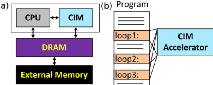
(a) (b)Fig. 1: The CIM-based architecture
accelerator. Figure 1(a) shows the concept; the CIM core may
consist of very dense memristive crossbar array and CMOS peripheral circuitry responsible for the communication and control from/to the crossbar. In a conventional computer, the memory access part of the executed applications is dominating the energy consumption and the performance degradation. If we manage to get this part executed within the CIM core, then significant energy and performance improvement can be realized. Figure 1(b) illustrates a program that could be executed efficiently on this architecture; multiple loops can be executed within the CIM core while the other parts of the program can be executed on the conventional core. It is worth stressing that computations in CIM core takes place
withinthe memory core consisting of amemory arrayand the
peripheral circuits. Therefore, depending onwhere the result
of the computation is produced, CIM core architecture can
be divided intoCIM-Array (CIM-A)[4,8] and CIM-Periphery
(CIM-P) [9,10]. Even though both CIM-A and CIM-P could
impact the design of the memory array, CIM-P entails a lesser impact on the design and hence is particularly attractive for a range of applications
This paper investigates three different application domains that could significantly benefit from the proposed architecture, and is organized as follows. Section II discusses the potential
of accelerating two data analytic application kernels,QUERY
SELECTfor database andXOR encryptionfor security
encryp-tion. Section III and Section IV investigate the speed-up for two signal processing applications (compressed sensing and recovery and advanced image processing) and two machine
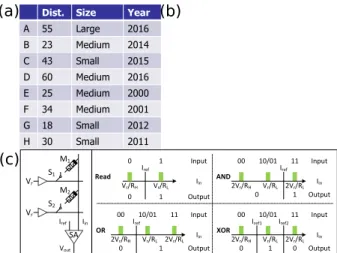
Dist. Size Year A 55 Large 2016 B 23 Medium 2014 C 43 Small 2015 D 60 Medium 2016 E 25 Medium 2000 F 34 Medium 2001 G 18 Small 2012 H 30 Small 2011 SA Vr Vr M1 M2 Iin Vout Vr/RL 2Vr/RL 2Vr/RH Iin 11 10/01 00 Input OR Output 1 0 S1 S2 Iref Iin Input Read Iref Output Vr/RH 0 0 Vr/RL 1 1 Iref Iin AND Iin XOR Iref1 Iref2 Output 0 1 Output 1 0 0 Vr/RL 2Vr/RL 2Vr/RH Vr/RL 2Vr/RL 2Vr/RH 11 10/01 00 Input Iref 11 10/01 00 Input (a) (b) (c)
Fig. 2: The database query problem and scouting logic
learning applications (deep learning inference for IoT sensory applications, and brain-inspired hyper-dimensional comput-ing), respectively. Section V concludes the paper.
II. CIMFOR DATA ANALYTICS
One of the potential applications is big-data analytics with a high percentage of logical operations that perform poorly on conventional architectures due to e.g., high cache miss rates. A. Targeted problem
We consider to speed up kernels (driven by bit-wise op-eration); examples are QUERY SELECT kernel (database applications) [11,12] and XOR encryption kernel (security encryption) [13].
• QUERY SELECT kernel: it performs the query-06 of
the TPC-H benchmark [11], which includes 22 queries written in SQL language. The query-06 performs compare instructions to check if the requested data is available in the database or not.
• XOR encryption kernel:it performs an XOR operation of
a string sequence and a predefined (secret) key. It is used for one-time-pad cryptography [14].
For QUERY SELECT kernel, we use a bitmap index scheme; it uses bitmaps (i.e., a vector of zeros and ones) to represent a database; generally they work well for low-cardinality columns. Figure 2(a) shows an example dataset with 8 entries, representing information of newly discovered stars. Each entry has three characteristics, i.e., distance (dist.), size and the year in which the star was discovered. Figure 2(b) presents the bitmap transposed representation of the same dataset, where the three characteristics (also called bins) are encoded into seven rows of zeros and ones; each column (e.g., A) is an entry while each row is a characteristic or bin. For example, a star with distance larger than 40 is defined as far, and otherwise as near. Typical database queries consist of searching for specific data patterns. These queries are carried out by performing bitwise operations on the bitmaps.
B. Implementation with CIM architecture
The implementation of CIM architecture considered for this application it similar to that shown in Figure 1; it consists of a conventional processor, main DRAM memory, novel data-centric CIM core and an external memory. Both the main memory and the CIM core can fetch data from the external memory. Like the main memory, CIM core is addressable from the processor and uses an extended address space. For simplicity, we assume that the data stored in the CIM core is not duplicated on the main DRAM memory; hence, simplified memory coherency schemes are required. The CIM core is initialized with data from the external memory, e.g., database(s); this initialization needs to be performed only once. The architecture implementation considered here belongs to CIM-P; i.e., computing within CIM takes place within the peripheral circuitry. For the considered application, computing consists mainly of performing bit-wise operations including OR, AND, XOR gates. Hence, the peripheral circuit should be
modified. It is equipped with Scouting Logic [15] illustrated
in Figure 2(c) using two binary valued memristive devices
programmed to resistance values R1 (for M1) and R2 (for
M2), respectively. Instead of reading a single memristive
device at a time, two (or more) inputs are activated
simulta-neously (e.g.,M1 andM2). The sensing current by the sense
amplifier depends on the equivalent input resistance (R1//R2).
By selecting appropriate reference currentsIref, the gates OR,
AND or XOR gates can be realized. C. Analysis of the potential
To evaluate the the potential of considered architecture in terms of (normalized) delay and energy, we developed two analytical models similar to that in [16]; one for conventional architecture and one for CIM architecture. Using an analytical evaluation model makes it faster to perform a design space exploration, although it could be less accurate. It is worth noting that the model for the two bit-wise driven applications considered here (QUERY SELECT kernel and XOR encryp-tion kernel) are similar; it is about the potential impact the CIM core on the overall performance rather than accurately quantifying the impact.
For the conventional architecture, we use the Intel Xeon E5-2680 multicore as a baseline with 4 cores, each with a frequency of 2.5GHz. Each core contains an ALU, and a two level cache (L1 of 32KB and L2 of 256KB). The cores share a main DRAM memory of 4GB. For the CIM architecture, we assume a single host processor with the same characteristics as an individual core in the conventional architecture. It contains an ALU, 32KB L1 cache and 256KB L2 cache, 1GB DRAM, and a CIM unit comprising 1,048,576 parallel memory arrays which has an area equivalent to that of 3GB DRAM. We
assume that a logical instruction takes ∼ 10ns on CIM core
which is equivalent to 20 CPU cycles [15,17].
We investigate the impact of the percentage of logical instructions accelerated by CIM core, as well as the impact of L1 and L2 cache miss rates on the potential improvement.
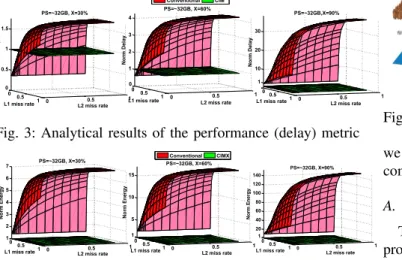
0 0.5 1 0 0.5 1 0 0.5 1 1.5 L2 miss rate PS=~32GB, X=30% L1 miss rate Norm Delay 0 0.5 1 0 0.5 1 0 1 2 3 4 L2 miss rate L1 miss rate Norm Delay CIM Conventional PS=~32GB, X=60% 00.5 1 0 0.5 1 1 10 20 30 L2 miss rate PS=~32GB,X=90% L1 miss rate Norm Delay
Fig. 3: Analytical results of the performance (delay) metric
00.5 1 0 0.5 1 1 2 3 4 5 6 7 L2 miss rate PS=~32GB, X=30% L1 miss rate Norm Energy 00.5 1 0 0.5 1 5 10 15 L2 miss rate L1 miss rate Norm Energy CIMX 1 Conventional PS=~32GB, X=60% 00.5 10 0.5 1 20 40 60 80 100 120 140 L2 miss rate PS=~32GB, X=90% L1 miss rate Norm Energy 1
Fig. 4: Analytical results of the energy metric Figure 3 shows the performance metric (defined by the nor-malized delay in seconds) for the conventional architecture (red planes) with respect to CIM architecture (green planes) for different percentages of accelerated instructions (X) on CIM core (ranging from 30 to 90%), assuming the problem
size of ∼32 gigabyte (GB). It can be seen that the larger the
size of the accelerated part on the CIM core, the higher the performance speed up; the speed up reaches up to 35x for the considered case. This can be clearly observed as the gap between the red and green planes increases. Moreover, the higher the miss rates, the higher the performance speed up of the CIM architecture. For low miss rates, the CIM could be even worse than conventional architecture especially when the percentage of accelerated instruction is low (e.g., 30% as Figure 3 shows).
Hence, the CIM architecture could be very suitable for applications with large data sizes and heavy memory access instruction (and bad data locality) resulting in a relatively high cache miss rate. Note that it has been shown that at least 30% of a database application could be accelerated using computation-in-memory [18].
Figure 4 shows the energy metrics (defined by the normal-ized energy in joule) for both architectures. Overall, similar trends are observed with respect to the percentage of accel-erated instructions. However, the energy consumption of the CIM architecture is always lower, irrespective of the cache miss rates. In case 30% of the instructions are accelerated, the conventional architecture consumes 6x more energy for the same problem size. This grows up to two orders of magnitude in case 90% of the instructions are accelerated. The high energy consumption of the conventional architecture can be partly attributed to the data movement and leakage current.
III. CIM FOR SIGNAL PROCESSING
Next, we will investigate the advantages of a CIM archi-tecture for applications such as advanced image processing and data compression. First, we will motivate an image processing application namely, guided image filter. Thereafter,
Fig. 5: Bilateral Filtering and Guided Filtering Processes [19] we will present a detailed investigation of the application of compressed sensing and recovery.
A. Image and video processing
The next generation of advanced image and video processing kernels often exhibit a mix of regular and irregular (or data-dependent) memory accesses. Moreover, they require data access which goes beyond the immediate
local neighbours. Typically, they need a medium-size
neighbourhood around the current pixel access. Typical
values can be from 7×7 up to 11×11 pixels of 23 bits
(in the case of colour images); and these do not directly fit in the local register-files, so they need to be accessed from SRAM caches or scratchpad memories. This limits the efficient mapping of these kernels on modern GPUs. The guided image filtering application [19] comprises a guidance
image I, a filtering input image p, and an output image q.
Both the guidance imageI and the input imagepact as input
to the application, and as a special case, they can even be identical. Figure 5 illustrates the bilateral and guided filtering process. The guided image filtering problem is ideally suited to be implemented in a CIM-P architecture. The essential idea is store the data in a large non-volatile memristive array and enable irregular memory access by modifying the address decoder of the memory macro.
B. Compressed sensing and recovery
1) Targeted problem: Reconstruction of a sparse
high-dimensional signal from low high-dimensional noisy measure-ments, for example received by sensor arrays, is used in many application fields, including radio interferometry for astronomical investigations, and magnetic resonance imaging, ultrasound imaging, and positron emission tomography for medical applications. Unfortunately, high-performance sparse signal recovery algorithms typically require a significant com-putational effort for the problem sizes occurring in most practical applications. While the computational complexity is not a major issue for applications where off-line processing on CPUs or graphics processing units can be afforded, it becomes extremely challenging for applications requiring real time processing at high throughput or for implementations on power-constrained devices.
In practically all the applications mentioned above, the observation model can be formulated as
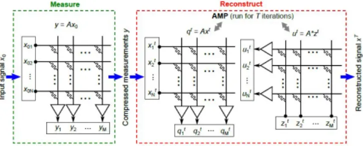
Fig. 6: Proposed CIM implementation of compressed sensing with AMP recovery
where A∈IRM×N is a known measurement matrix,x0∈IRN
is the signal of interest, y ∈ IRM is the measurement data
vector and w ∈IRM represents the measurement noise. The
goal is to recoverx0from y when M<N. A first order
approx-imate message passing (AMP) technique for reconstructingx0
given y [20] may be represented as
zt=y−Axt+ N
Mz t−1
η0t−1(A∗zt−1+xt−1)
xt+1=ηt(A∗zt+xt)
wherext ∈IRN is the current estimate ofx0 at iteration t,
zt ∈ IR M is the current residual,A∗ is the transpose of A,
ηt(·) is a function, η0t(·) its derivative, h·i denotes the mean
andx0= 0. The final value of xt provides the estimate ofx
0.
The AMP algorithm has a relatively simple formulation and requires only multiplications and additions, making it suitable for a memristive CIM architecture.
2) Implementation with CIM architecture: A CIM
archi-tecture comprising CIM-P-type units that can store the
mea-surement matrix A and perform the matrix-vector
multi-plications within the array would significantly increase the
area/time/power efficiency. The elements of A are mapped
as conductance values of memristive devices organized in a crossbar array, as depicted in Figure 6 [21]. One possible method to program the conductance values is by an iterative program-and-verify procedure. The compressed measurements
y are acquired by applying x0 as voltages to the crossbar
rows via digital-to-analog conversion, and obtainingythrough
analog-to-digital conversion of the resulting output currents at columns. The positive and negative elements of A can be coded on separate devices together with a subtraction circuit, whereas negative vector elements can be applied as negative voltages.
Once the matrixAis programmed in the crossbar array and
the measurementsyare obtained, the AMP algorithm is run in
a dedicated processing unit, while the computation ofqt=Axt
and ut=A∗zt is performed using the (same) crossbar array.
The vector qt is computed by applying xt as voltages to the
rows and reading back the resulting currents on the columns,
andutby applyingztas voltages to the columns and reading
back the resulting currents on the rows.
In the AMP algorithm, ignoring theηt(·) andη0t(·) functions,
the main computational cost comes from the matrix-vector
TABLE I: FPGA resource utilization, frequency and estimated dynamic on-chip power consumption
LUT FF BRAM f[MHZ] Pstatic[W] Pdynamic[W]
307908 180368 1024 200 4.04 26.4
[46.4%] [13.6%] [47.4%] (utilization on the xckul 15 FPGA device)
multiplications Axt and A∗zt which both require O(M N)
operations for dense A. The other operations in the AMP
algorithm are vector additions and multiplications which
re-quire O(N) operations. Thus, one could potentially reduce the
complexity of AMP from O(M N) to O(N) by performing
Axt andA∗zt in memristive arrays, assuming that η
t(·) and η0
t(·) involve only O(N) or less operations. The expectation
is that in a memristive crossbar, matrix-vector multiplications
can be performed with constant time complexity O(γ), where
γ is independent of the crossbar size.
3) Analysis of the potential: To quantify the potential
en-ergy gains of the CIM implementation over a conventional de-sign, based on the figures currently achieved with a prototype phase-change memory (PCM) chip [22], we made an FPGA design that operates at the same speed and the same precision at which we expect a PCM-based crossbar to perform. In the AMP algorithm, the matrix-vector multiplications are the most expensive operations, so we compared the memristive crossbar analog multiplier with a 4-bit FPGA multiplier design. We fo-cus in this analysis on the energy drawn by the computational units and disregard the time and power consumption of the data transfers.
The time to compute one dot-product is equal to the vector size divided by 8, plus 5 cycles to complete the pipeline.
For a1024×1024matrix-vector product using the 1024-unit
design, each dot-product unit stores one of the matrix row of 1024 elements encoded with 4-bit per value in the local 32Kbit BlockRAM. To read the row vector from memory and to perform the dot-product operation takes a total of 133 clock cycles. Hence, it takes 665 ns to complete one matrix-vector multiplication at a clock frequency of 200 MHz. Considering a dynamic power consumption of 26.6W, one matrix-vector
multiplication consumes 17.7µJ on the FPGA.
In a memristive crossbar of size1024×1024based on PCM
devices, the dynamic power dissipation in the devices for one READ operation is expected to be on the order of 0.21W,
assuming an average READ current of 1µA per device and
average voltage of 0.2V. In order to operate this crossbar at 1µs
cycle time, 8 analog-to-digital converters (ADCs) operating at 125MSps are needed to read the currents from all 1024
columns in approximately 1µs. The power consumption of
8-bit ADCs in 90nm technology is estimated to be around 12 mW/GSps, thus 12.3mW for 1024 reads per microsecond. Therefore, the total power consumption of the crossbar and ADCs is estimated to be around 222mW, which is 120 times lower than the 4-bit FPGA design. The energy per READ is 222nJ, which is 80 times lower than the FPGA. Assuming
90nm technology and 25F2 1T1R PCM cells (F = 90nm), the
area occupied by a 1024x1024 crossbar and 8 ADCs (each of
Always ON NN Network of Sensors Normally OFF High-end CPU W ak es Battery or harvested Standard power domain 1.E-11 1.E-10 1.E-09 1.E-08 1.E-07 1.E-06 1.E-05 1.E-04 1.E-03 32 64 128 256 512 Tot al Ener gy (J)
Fully-Connected Network Dimensions (N^2)
4-bit ADC
Sub-Vth CM0 10pJ/cycle
VnomCM0 (100pJ/Cycle)
(a) (b)
Fig. 7: Inference on IoT sensory devices IV. CIM FOR MACHINE LEARNING
In this section, we will investigate the application domain of machine learning in particular applications where the training or inference has to be performed in highly energy/area con-strained environments. First, we will present the application domain of deep learning for internet-of-things (IoT) and subsequently, we will present the emerging machine learning paradigm of hyperdimensional computing.
A. Deep learning inference for IoT sensory applications
1) Targeted problem: Computing systems with CIM
archi-tectures could play a key role in the Internet of things (IoT) sensory domain. When deployed in edge-devices, always ON deep learning inference applications require minimum power consumption, and therefore, CIM architectures particularly suit these hard requirements. Examples include Human Activity Recognition (HAR), Key Word Spotting (KWS) and online Electro-cardiograph (ECG) event detection and classification. As shown in Figure 7(a), the always ON CIM architectures can process the data coming from a network of sensors in an efficient manner, and either work as the main computing element on the IoT device, or on the other hand, sparsely wake up a higher-end CPU should a specific condition be met.
2) Implementation with CIM architecture: Similar to the
compressed sensing application, the computational primitive is matrix-vector multiplication using a memristive crossbar array. Deep neural networks are just a cascade of matrix-vector multiply units and activation functions. The multiple layers of a standard fully connected neural network (FCNN) or convolutional neural network (CNN) can be mapped to CIM cores comprising memristive crossbar arrays. Even though the matrix-vector multiplications are performed in the analog domain using Ohms law and Kirchhoffs current summation law, DACs are used to input the data to each crossbar array and ADCs are used to digitize the resulting current. A key challenge is the lack of precision associated with the analog multiplication as well as the quantization of the input and activations as dictated by the DAC/ADC resolution. However, it has recently been demonstrated that it is possible to perform deep learning inference with limited precision. It is shown that one can achieve comparable classification accuracy as networks operating with floating point precision [23].
3) Analysis of the potential: Preliminary comparative study
of implementations of the DL algorithms was conducted. First, we analyzed the effects that low precision layers have on the overall NN accuracy, determining the quantization char-acteristics of the different layers. Second, the CIM approach
HD Mapping: Item memory HD Encoding: MAP operations Associative memory Letter d-bit
Labels: languages with 21 classes
d-bit Training or classification d-bit Preprocessing Channel 1 HD Mapping: Item memory
HD Encoding: MAP Operations
Associative Memory d-bit
Labels: hand gestures with 5 classes
Training or classification … … … d-bit Preprocessing Channel 4 HD Mapping: Item memory
(a)
(b)
Fig. 8: General and scalable HD computing for various learn-ing and classification tasks
was compared with implementations using low-power near threshold Cortex-M processors [24]. The study shows the significant potential for energy gains with the use of a low precision CIM architecture (see Figure 7(b)).
B. Brain-inspired hyper-dimensional computing
1) Targeted problem: We present another application space
for CIM namely hyperdimensional (HD) computing suitable for various learning and classification tasks using memristive devices [25]. HD computing is a brain-inspired computing paradigm where information is represented in hypervectors:
d-dimensional holographic (pseudo)random vectors with
inde-pendent and identically distributed (i.i.d.) components. When
the dimensionality is in the thousands, e.g. d >1000, there
exist a very large number of quasiorthogonal hypervectors. This lets HD computing combine such hypervectors into a new hypervector using well-defined vector space operations. These mathematical operations are bitwise and ensure that the resulting hypervector has the same dimensionality—i.e., fixed-width. The resulting hypervectors can then be directly used to not only classify but also to bind, associate, and perform other types of “cognitive” operations in a straightforward manner.
HD computing uses three operations to combine binary hy-pervectors: addition (which can be weighted), multiplication, and permutation (more generally, multiplication by a matrix) that are collectively called as MAP operations. “Addition” and “multiplication” are meant in the abstract algebra sense where
the sum of binary hypervectors[A+B+. . .]is defined as the
componentwise majority function with ties broken at random, the product is defined as the componentwise XOR (addition
modulo 2, ⊕), and permutation (ρ) shuffles the components.
All these MAP operations produce a d-bit hypervector.
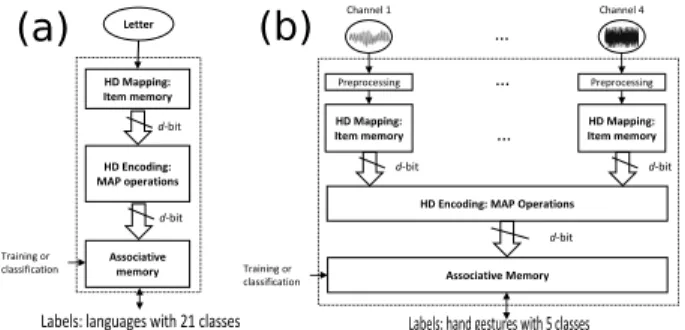
HD computing has been used in various applications such as language recognition [26] (Figure 8(a)) and biosignal pro-cessing (Figure 8(b)) including electromyography (EMG) [27], electroencephalography (EEG) [28], and electrocorticography (ECoG) [29] with up to 100 electrodes. These learning and classification tasks are based on the same hardware construct: 1) mapping to the HD space, 2) encoding with the MAP operations, and 3) associative memory (see Figure 8). During training, the associative memory updates the learned patterns with new hypervectors, while during classification it computes distances between a query hypervector and learned patterns.
Hence, it is possible to build a CIM engine based on these operations to cover a variety of tasks.
2) Implementation with CIM architecture: The CIM
prim-itives used for HD computing implementation are dot-product and bitwise operations. The dot-product is performed using binary input values, binary memristor states, and analog output. The bitwise operations are performed using binary input values, binary memristor states, and binary output. The memristor values are written only once before the execution of the HD algorithm and are never modified again. Additional digital computations and memory buffers are needed in order to implement the entire HD algorithm.
3) Analysis of the potential: Simulation studies were
con-ducted using a CIM unit based on realistic models of phase-change memory devices. It was shown the CIM architec-ture can deliver comparable accuracies to the ideal software simulations for the task of language recognition. Preliminary results were also obtained comparing the energy efficiency of a potential CIM-based implementation over 65nm digital CMOS implementation. A cycle-accurate RTL model that has equivalent throughput to that of the proposed CIM HD proces-sor was developed. The RTL model was synthesized in UMC
65nm technology node using Synopsys Design Compiler.
Energy estimation was carried out in Synopsys PrimeTime
by providing the netlist and the activity file as the inputs.
A best area improvement of 9×and an energy improvement
of 5× is expected with the CIM HD processor architecture
compared to CMOS counterpart. By utilizing more efficient ADCs the performance numbers could be improved further. Nevertheless if only the replaceable module in the architecture are considered vast improvements can be expected which are eclipsed by the current energy budget of the non-replaceable modules. When only replaceable modules are considered, energy efficiency can be two to three orders of magnitude higher in the case of a CIM architecture.
V. CONCLUSION
Computation-in-memory using memristive devices is an emerging computing paradigm that tries to address the chal-lenge of memory wall posed by the conventional von Neu-mann architecture. Although the extent of improvement in terms of energy/time efficiency is application and problem-size dependent, the CIM architecture clearly has the potential to outperform the traditional von Neumann architecture due to many reasons. For instance, it uses non-volatile memristive technology which reduces the static power. In addition, it performs computation within the memory core, meaning that data movement is significantly reduced; this results both in energy saving and performance improvement. Moreover, given the nature of the CIM core, the time complexity of some primitive function such as matrix-vector multiplication could
be reduced from O(N2) to O(1), resulting in further
per-formance improvement. In this paper, we presented concrete examples from the domains of data analytics, signal processing and machine learning that could significantly benefit from this new architecture. We presented how a CIM architecture
could tackle these problems and in many instances presented a detailed study on the potential area/energy/time benefits.
REFERENCES
[1] Patterson, “Future of computer architecture,” inBerkeley EECS Annual
Research Symposium (BEARS), US, 2006.
[2] Jones, “Whitepaper: semiconductor industry from 2015 to 2025,”
Inter-national Business Strategies, 2015.
[3] Hamdiouiet al., “Memristor based computation-in-memory architecture
for data-intensive applications,” inDATE’15, 2015, pp. 1718–1725.
[4] Sebastian et al., “Temporal correlation detection using computational
phase-change memory,”Nature Communications, vol. 8, p. 1115, 2017.
[5] Sebastianet al., “Tutorial: Brain-inspired computing using phase-change
memory devices,”Journal of Applied Physics, vol. 124, p. 111101, 2018.
[6] “https://www.research.ibm.com/ibm-q/.”
[7] ITRS, “Beyond cmos white paper,” ITRS, Tech. Rep., 2014.
[8] Hosseini et al., “Accumulation-based computing using phase-change
memories with fet access devices,” IEEE Electron Device Letters,
vol. 36, pp. 975–977, 2015.
[9] Du Nguyenet al., “Memristive devices for computing: Beyond cmos
and beyond von neumann,” inVLSI-SoC’17. IEEE, 2017.
[10] Li et al., “Pinatubo: A processing-in-memory architecture for bulk
bitwise operations in emerging non-volatile memories,” in DAC’16.
IEEE, 2016.
[11] Council, “Tpc-h, a decision support benchmark,” 2015.
[12] Wu et al., “Using bitmap index for interactive exploration of large
datasets,” inSSDBM’03. IEEE, 2003, pp. 65–74.
[13] Yang et al., “Improving memory encryption performance in secure
processors,”IEEE Trans. on Comp., vol. 54, pp. 630–640, 2005.
[14] Yanget al., “Memristive devices for computing,”Nature
nanotechnol-ogy, vol. 8, pp. 13–24, 2013.
[15] Xieet al., “Scouting logic: A novel memristor-based logic design for
resistive computing,” inISVLSI’17. IEEE, 2017, pp. 176–181.
[16] Du Nguyenet al., “On the implementation of computation-in-memory
parallel adder,”IEEE TVLSI, 2017.
[17] PS.Yu, “merging memory technologies,”SPRING 2016 Solid-sate
cir-cuits magazine, vol. 8, pp. 43–56, 2016.
[18] Seshadriet al., “Fast bulk bitwise and and or in dram,”IEEE Computer
Architecture Letters, vol. 14, pp. 127–131, 2015.
[19] He et al., “Guided image filtering,” IEEE transactions on pattern
analysis & machine intelligence, pp. 1397–1409, 2013.
[20] Donohoet al., “Message-passing algorithms for compressed sensing,”
Proceedings of the National Academy of Sciences, vol. 106, pp. 18 914– 18 919, 2009.
[21] Le Galloet al., “Compressed sensing with approximate message passing
using in-memory computing,”IEEE Transactions on Electron Devices,
vol. 65, pp. 4304–4312, 2018.
[22] Le Galloet al., “Mixed-precision in-memory computing,”Nature
Elec-tronics, vol. 1, p. 246, 2018.
[23] Zhou et al., “Incremental Network Quantization: Towards Lossless
CNNs with Low-Precision Weights,” pp. 1–14, Feb 2017. [Online]. Available: http://arxiv.org/abs/1702.03044
[24] Myerset al., “A 12.4pJ/cycle sub-threshold, 16pJ/cycle near-threshold
ARM Cortex-M0+ MCU with autonomous SRPG/DVFS and
tempera-ture tracking clocks,” inSymposium on VLSI Circuits. IEEE, jun 2017,
pp. C332–C333.
[25] Rahimi et al., “High-dimensional computing as a nanoscalable
paradigm,”IEEE TCAS I, vol. 64, pp. 2508–2521, Sept 2017.
[26] Rahimi et al., “A robust and energy efficient classifier using
brain-inspired hyperdimensional computing,” in Symposium on Low Power
Electronics and Design, August 2016.
[27] Rahimiet al., “Hyperdimensional biosignal processing: A case study
for EMG-based hand gesture recognition,” inIEEE International
Con-ference on Rebooting Computing, October 2016.
[28] Rahimi et al., “Hyperdimensional computing for noninvasive brain–
computer interfaces: Blind and one-shot classification of EEG
error-related potentials,”BICT’17, 2017.
[29] Burrelloet al., “One-shot learning for iEEG seizure detection using
end-to-end binary operations: Local binary patterns with hyperdimensional