DESIGN OF LARGE TIME-CONSTANT SWITCHED-CAPACITOR
FILTERS FOR BIOMEDICAL APPLICATIONS
A Thesis by
SANJAY TUMATI
Submitted to the Office of Graduate Studies of Texas A&M University
in partial fulfillment of the requirements for the degree of MASTER OF SCIENCE
December 2004
DESIGN OF LARGE TIME-CONSTANT SWITCHED-CAPACITOR
FILTERS FOR BIOMEDICAL APPLICATIONS
A Thesis by
SANJAY TUMATI
Submitted to Texas A&M University in partial fulfillment of the requirements
for the degree of MASTER OF SCIENCE Approved as to style and content by:
Jose Silva-Martinez
(Chair of Committee) Ugur (Member) Cilingiroglu
Prasad Enjeti
(Member) Jay R. Porter (Member)
Chanan Singh (Head of Department)
December 2004
ABSTRACT
Design of Large Time-Constant Switched-Capacitor Filters for Biomedical Applications.
(December 2004)
Sanjay Tumati, B.Tech., Indian Institute of Technology, Mumbai, India Chair of Advisory Committee: Dr. Jose Silva-Martinez
This thesis investigates the various techniques to achieve large time constants and the ultimate limitations therein. A novel circuit technique for the realization of large time constants for high pass corners in switched-capacitor filters is also proposed and compared with existing techniques. The switched-capacitor technique is insensitive to parasitic capacitances and is area efficient and it requires only two clock phases. The circuit is used to build a typical switched-capacitor front end with a gain of 10. The low pass corner is fixed at 200 Hz. The high pass corner is varied from 0.159Hz to 4 Hz and various performance parameters, such as power consumption, silicon area etc., are compared with conventional techniques and the advantages and disadvantages of each technique are demonstrated. The front-ends are fully differential and are chopper stabilized to protect against DC offsets and 1/f noise. The front-end is implemented in AMI0.6um technology with a supply voltage of 1.6V and all transistors operate in weak inversion with currents in the range of tens of nano-amperes.
DEDICATION
ACKNOWLEDGEMENTS
I gratefully acknowledge my advisor Dr. Jose Silva-Martinez for giving me great freedom in choosing a thesis topic and then patiently answering my queries and keeping me on the right track. Dr. Silva has this amazing ability to quickly penetrate the core of any circuit which would elude me for weeks. This ability of his used to be a great source of embarrassment to me (and as I later found out, to almost everyone who had technical discussions with him). However, it was possibly the best training I could get in analyzing circuits in an intuitive non-mathematical way. I am also thankful to Dr. Jay R. Porter who has been my employer, an excellent one at that, for almost my entire stay at A&M. I would like to thank David Genzer, Dr. Ashok Nedungadi and Dr. Lee Hudson of Biotronik GmBh for giving me an opportunity to intern with them. They effectively suggested my thesis topic and addressed many practical issues and concerns that I have had. I would like to thank Dr. Cilingiroglu for his excellent course on device physics. Thanks to him, I am no longer afraid of device physics. His friendly manner and his humility in spite of his apparent genius for device physics have made a deep impression on me. Finally, I would like to thank my father for keeping me calm when things threatened to overwhelm me and my mother for constantly calling me and asking me if I was done with my thesis already. Without this kind of outside support, this thesis would never have been completed.
TABLE OF CONTENTS
Page
ABSTRACT ... iii
DEDICATION ...iv
ACKNOWLEDGEMENTS ...v
TABLE OF CONTENTS ...vi
LIST OF FIGURES...ix
LIST OF TABLES ... xiii
CHAPTER I INTRODUCTION...1
1.1 Motivation ...1
1.2 On-chip Implementation……….4
1.3 The Switched-Capacitor Circuitry………..6
II OTA DESIGN……….9
2.1 Operation in Weak Inversion………..9
2.2 The Folded-Cascode OTA………....11
2.3 The Single-Stage OTA……….15
2.4 Mismatches in OTA Transistors………...16
2.5 Conclusions………...19
CHAPTER Page
3.1 Conventional Integrator………20
3.2 Fleischer-Laker (FL) Biquad……….22
3.3 The T-Cell Method………30
3.4 The Split-Integrating Capacitor Technique………...32
3.5 The Nagaraj Technique……….39
3.6 Combining the FL Biquad with the Nagaraj Integrator………....46
3.7 Conclusions………...51
IV LARGE TIME CONSTANTS IN SC HIGH PASS FILTERS………….52
4.1 Realizing a Differentiator ……….53
4.2 Basic High Pass Filter………...54
4.3 Partial Positive Feedback………..57
4.4 Attenuated Feedback HPF………....61 4.5 Differentiators………...71 4.6 Noise Analysis……….….73 4.7 Comparisons……….…79 4.8 Conclusions………...84 V PRE-AMP DESIGN...85
5.1 Introduction and Specifications………....85
5.2 Pre-amp Using the Proposed HPF………86
CHAPTER Page
5.4 The Nagaraj Low Pass Filter...98
5.5 Charge Injection and Leakage...101
5.6 Clock Feed-Through ...102 5.7 Comparisons...106 5.8 Layout...108 5.9 Simulation Results...109 VI CONCLUSIONS…...……….121 REFERENCES...123 VITA ...125
LIST OF FIGURES
Page
Fig. 1-1. Experimental pacemaker...2
Fig. 1-2. High level block diagram of pacemaker pre-amp...5
Fig. 2-1. Conventional fully differential folded-cascode OTA ...12
Fig. 2-2. Switched-capacitor CMFB circuit ...13
Fig. 2-3. Conventional fully differential single-stage OTA ...15
Fig. 2-4. Chopper stabilization to chop the OTA offsets to higher frequencies...17
Fig. 2-5. The effect of chopper stabilization on an ideally stationary output...18
Fig. 3-1. Conventional SC lossless integrator ...20
Fig. 3-2. Conventional Fleischer-Laker biquad for low Q applications ...22
Fig. 3-3a. Loading configuration for OTA 2 of Fig. 3-2 during phase 2 ...28
Fig. 3-3b. Circuit of Fig. 3-3a with feedback loop opened...28
Fig. 3-4. Conceptual implementation of large integrator time constants ...30
Fig. 3-5. Large TC integrator using the T-Cell technique ...31
Fig. 3-6. Conceptual diagram of the split-integrating capacitor technique ...32
Fig. 3-7. SC implementation of the concept shown in Fig. 3-6...34
Fig. 3-8. Conceptual implementation of large TC LPF ...35
Fig. 3-9. A large time constant integrator in the FL biquad ...36
Fig. 3-10. The Nagaraj integrator ...39
Page
Fig. 3-12. Illustrating the voltage waveforms in the Nagaraj integrator ...41
Fig. 3-13. The Nagaraj low pass filter ...42
Fig. 3-14. FL biquad using the Nagaraj integrator ...47
Fig. 4-1. Conventional SC differentiator ...53
Fig. 4-2. Conventional continuous time high pass filter...54
Fig. 4-3. Conventional SC high pass filter ...55
Fig. 4-4. Illustrating loading by breaking the feedback loop in Fig. 4-3…………...56
Fig. 4-5. Conceptual partial positive feedback ...57
Fig. 4-6. Simple SC implementation of partial positive feedback...58
Fig. 4-7. A sophisticated implementation of partial positive feedback ...59
Fig. 4-8. Conceptual attenuated feedback...61
Fig. 4-9. Conceptual SC implementation of attenuated feedback ...62
Fig. 4-10. The T-Cell technique adapted to high pass filters...63
Fig. 4-11. Attenuated feedback in SC HPFs using two OTAs ...64
Fig. 4-12. Fully differential LTC SC HPF using only one OTA...65
Fig. 4-13a HPF of Fig. 4-12 in phase 2 performing attenuation ...66
Fig. 4-13b HPF of Fig. 4-12 in phase 1 performing high pass filtering ...66
Fig. 4-14. Loading on OTA of Fig. 4-12 during phase 1...69
Fig. 4-15. Transient waveforms for the structure of Fig. 4-12 ...70
Fig. 4-16. Large time constant SC differentiator...72
Page
Fig. 4-17b. The CT LPF ...75
Fig. 4-17c. HPF implementation using buffers and an LPF...76
Fig. 4-17d. CT FL biquad ...77
Fig. 4-18. Power comparison plots ...81
Fig. 4-19. Capacitor area comparisons ...82
Fig. 4-20. Noise comparison plots...83
Fig. 5-1. Block diagram of pacemaker pre-amp ...86
Fig. 5-2. Pre-amp using proposed fully differential HPF ...87
Fig. 5-3. Pre-amp using attenuated feedback HPF and OTA reuse ...88
Fig. 5-4. Pre-amp using FL biquad and Nagaraj integrator ...94
Fig. 5-5. Pre-amp implementation using Nagaraj LPF and OTA reuse………..…...98
Fig. 5-6a. The Nagaraj LPF………104
Fig. 5-6b. Nagaraj integrator………..105
Fig. 5-6c. Proposed HPF………105
Fig. 5-7. Power consumption of the three pre-amps, INAGARAJ=IFL-NAGARAJ……….106
Fig. 5-8. Capacitor area of the three pre-amps………...………….………..107
Fig. 5-9. HPF based pre-amp layout……….……….108
Fig. 5-10a. PSS response showing high pass corner………..……….……….110
Fig. 5-10b. PSS response showing low pass corner……..….……….……….110
Fig. 5-10c. Complete PSS response for the proposed pre-amp….…..……….…111
Page
Fig. 5-11b. Complete PSS response of FL biquad showing the low pass corner…...112
Fig. 5-12a. PSS response showing high pass corner………...113
Fig. 5-12b. PSS response showing low pass corner….……….…..114
Fig. 5-13a. CMRR in presence of 5% path loading mismatch………116
Fig. 5-13b. CMRR in presence of 1% ratio mismatch………....116
Fig. 5-13c. PSRR in presence of 5% ratio mismatch………..117
Fig. 5-13d. PSRR in presence of 1% ratio mismatch……….…….117
Fig. 5-14a. Demonstrating output swing in the OTA………...…..…….118
Fig. 5-14b. Demonstrating linearity via FFT. THD > 40dB……….…...119
LIST OF TABLES
Page
Table 3-1. Capacitor values for FL biquad of Fig. 3-2...25
Table 3-2. Capacitor values for Fig. 3-9, DNM stands for does not matter ...37
Table 3-3. Capacitor values for Fig. 3-13 optimizing spread ...43
Table 3-4. Capacitor values for Fig. 3-13 optimizing area...44
Table 3-5. Capacitor values for Fig. 3-14 optimizing spread ...49
Table 3-6. Capacitor values for Fig. 3-14 optimizing loading on opa-2 ...49
Table 4-1. Capacitor values for Fig. 4-12.………….………...……….67
Table 4-2. Table of comparisons for various structures for a 4Hz 3-dB corner..…..79
Table 4-3. Comparison table for various structures for a 0.159 Hz 3 dB corner……80
Table 5-1. Capacitor values for Fig. 5-3 for a 4 Hz high pass corner..………..90
Table 5-2. Capacitor values for Fig. 5-3 for a 0.159 Hz high pass corner ….……...91
Table 5-3. Capacitor values for Fig. 5-4 for a 4 Hz high pass corner ….…………..96
Table 5-4. Capacitor values for Fig. 5-4 for a 0.159 Hz high pass corner ………....97
Table 5-5. Capacitor values for Fig. 5-5 for a 4 Hz high pass corner ……...……..100
CHAPTER I
INTRODUCTION
1. INTRODUCTION1.1 Motivation
The realization of large time constants on-chip is of considerable interest in biomedical and electrochemical applications, which require real time processing of analog voltages [1]. One example is a pre-amp used in a pacemaker circuit. Other examples include some biomedical applications in which stand alone differentiators and high pass filters are required [2,3]. In this thesis, we explore the problem of large time constants and present some novel differentiators and high pass structures, which realize large time constants. The novel structures will be used in a biomedical switched-capacitor pre-amplifier, which is used in pacemaker circuits.
In pacemaker circuits, whenever the heart is given a pacing pulse, the heart responds through a set of signals. The response of the heart to a pacing pulse is referred to as the evoked response. This response is first captured by the analog front-end, amplified, filtered and fed to the DSP core. The DSP core performs signal processing on this amplified and filtered version of the response and the decision circuit uses the results of this processing. A block level schematic of a pacemaker [4] is given in Fig. 1-1. To make an intelligent decision, the pacemaker front end needs to capture as much information as possible in the evoked response.
_____________
Sw it ch M a tr ix To
Fig. 1-1: Experimental pacemaker
The front end is basically a filter, which provides amplification to the evoked response. The input to the front end comes from the leads that are connected to the various chambers of the heart (left/right atrium/ventricle). The wideband analog front-End consists of all circuits up to the Narrow-Band Band-pass filter and the ADC.
The front end includes the following:
1. High input impedance buffers so as not to load the heart chambers.
2. A switch matrix to multiplex the inputs from the leads. There are a total of 8 input leads. Only two have been shown in Fig. 1.1.
3. The first HPF, which consists of a differential amplifier providing a gain of 10 and passive RC components.
4. The first LPF, which consists of a buffer and passive RC components. 5. A second HPF incorporating a gain of 5.
Le a d s Pacing Circuits Narrowband Bandpass Filter Threshold Detector A/D Converter processor and Control Logic Buffers HPF LPF HPF LPF
6. A second LPF incorporating a gain of 2.
7. A buffer at the end to interface with the narrow band filter and the rest of the digital circuitry.
8. One must have also observed a large number of switches in what appears to be continuous time circuitry. The reason for the switches is that the Front end must be switched on gradually. First the high pass switches on and is given some time to settle down to its steady state. Once the high pass settles, the low pass filter switches ON and so on and so forth. The reason for switching on the front-end gradually is that if a large device with such high open loop gain is switched on all at once, there will be a considerable amount of ringing. And this ringing might bury the evoked response.
It must be mentioned here that Fig. 1-1 is only a conceptual discrete implementation. The actual on-chip implementation will be considerably different as will be discussed later in this chapter.
The evoked response contains useful information in frequencies less than 1Hz. The information can be processed by the DSP in the pacemaker to decide on whether a pacing pulse must be given to the heart. More sophisticated pacemakers are expected to decide on even the amplitude and duration of the pacing pulse. Since the pulse generator in the pacing circuit consumes so much power, it is not desirable to give the heart a pacing pulse when it is not needed. Thus the front-end needs to capture the evoked response with a fair amount of accuracy, i.e. low distortion, high SNR and accurate filter corners. Currently the biomedical industry uses front-ends with a high pass corner of 4
Hz and a low pass corner of 200 Hz with a clock frequency of 2.5KHz. The main aim is to push the high pass corner to sub-hertz frequencies.
1.2 On-chip Implementation
The block diagram in Fig. 1-1 shows the discrete realization of the pacemaker front-end. However, an on-chip realization is required. The problem with on-chip implementations is that precise resistors and capacitors are not available on-chip in most CMOS processes. Typically the RC time-constant varies by 20%. Thus, either Laser trimming is required for on-chip passive components or else they have to go off-chip. Both options are expensive.
Switched-capacitor implementations can offer very accurate time constants and are thus ideal for low frequency applications such as pacemaker circuitry. Another advantage is that switched-capacitor circuits are very linear. Continuous time circuits based on transconductances inherit their non-linearity from the MOS transistor. Switched-capacitor circuits are much less dependent on the non-linearity of the MOS transistor.
However, we cannot completely eliminate the continuous time circuitry. The reason is that switched-capacitor circuits cause aliasing (down-conversion) of high frequency noise to low frequencies and degrade the SNR. Thus a continuous time anti-aliasing low pass filter will always be required to attenuate the high frequency noise before it is aliased by the switched-capacitor circuitry. Fig. 1-2 shows a high level block diagram of an on-chip pacemaker pre-amp.
Continuous-Time
Circuitry
Switched
Capacitor
Circuitry
Heart Signal, V1 Heart Signal, V2 Vx VoutFig. 1-2: High level block diagram of pacemaker pre-amp
The continuous time circuitry consists of:
1. A low noise gain stage of 10. This ensures that the noise of succeeding stages is less important. This is similar to the use of Low Noise amplifiers in RF front-ends.
2. A high pass filter to remove the offsets, which are residues from the pacing pulse. 3. A low pass anti-aliasing filter.
The switched-capacitor circuitry consists of a high pass filter, a low pass filter and an amplifier with a gain of 10. Thus the complete front end has a second order roll off for both the high pass and low pass corners and a combined gain of 100.
1.3 The Switched-Capacitor Circuitry
Our focus here is the switched-capacitor circuitry and the problem of realizing large time constants therein. The switched-capacitor circuitry has a gain of 10, a low pass corner of 4Hz and a high pass corner of 200 Hz. In addition, the continuous time circuitry is followed immediately by a switched-capacitor S/H hold stage to isolate the continuous
time circuitry from the switched-capacitor circuitry. A S/H stage is used as a buffer between the blocks to prevent loading on the continuous circuitry and the switched-capacitor circuitry.
The realization of large time constants is the main bottleneck in the design of the front-end. The clock frequency is 3-4 orders of magnitude larger than the high pass corner. Two factors are involved in the selection of 2.5 KHz as the clock frequency. One is the low pass corner (quite high at 200 Hz) and the other is the need to maintain compatibility with the rest of the system. If conventional switched-capacitor structures are used in the above applications, the capacitor ratios tend to be large enough to discourage their implementation in integrated circuits.
Many techniques have been proposed to implement large time constants [5-9]. These techniques will be discussed in subsequent chapters. All of the techniques are for use in integrators or in first order low pass sections. To the author’s knowledge, there is no technique yet to achieve large time constants in first order high pass sections or differentiators. Switched-capacitor differentiators are used in audio codecs and in some biomedical applications [2,3]. It is quite intuitive that the best way to achieve a high pass corner is through the use of high pass sections rather than by combining low pass sections and amplifiers. We will see that this intuition holds in some cases, but not in others.
Conventionally, there are two methods to achieve a high pass corner in switched-capacitor circuits.
1. Band-pass biquads: Biquads are usually used in narrow band filtering applications where complex poles are required. In pacemaker applications, the front-end is a wideband filter and hence it is hard to justify using a biquad. One reason is that wideband transfer functions realized using Bi-quads have a greater passband ripple than by using first order sections. The other reason is that in wideband applications, biquads introduce greater errors than first order sections. Biquads, in general, also have lower dynamic range than first order sections. Further, in any implementations of band pass functions using ideal biquads, the zero of the transfer function is at DC. However, in real biquads, due to finite DC gain of the op-amps, the zero of the transfer function is not at DC. Rather, it is at a low frequency. This low frequency zero introduces an error in the 3-dB high pass corner, especially if that 3-dB corner is at a very low frequency. This statement will be proved further in Chapter II when we discuss biquad implementations of large time constants. Thus the error (in the corner) would be greater in a bi-quad. Nevertheless, the Fleischer-Laker biquad can achieve wide band operation. Indeed, the Fleischer-Laker biquad is widely used in single ended applications where DC offset is a problem. In differential ended applications, these offsets are largely eliminated by the common mode feedback circuitry.
2. First order sections: A high pass corner can be achieved, by designing a low pass filter with the same low pass corner as the desired high pass corner and then subtracting from a buffer or a gain stage as illustrated in the equations below
. ) ( 1 ) ( 1 1 ) ( ρ ρ + = − = + = s s s H s H s s H LPF HPF LPF (1.1)
If by some way, we could build a first order high pass section, we could eliminate the buffer or the gain stage and thus save power. This provides our motivation for coming up with a new scheme to realize large time constants in high pass sections.
CHAPTER II
OTA DESIGN
8 CONCLUSIONS2.1 Operation in Weak Inversion
Biomedical applications are very low frequency applications. Thus the operational transconductor amplifiers (OTAs) used in switched-capacitor circuits for such applications have a much greater amount of time for settling. For this reason, the transistors in biomedical applications operate in weak inversion and carry currents in the nano-ampere range. Usually, the OTA power requirements in switched-capacitor applications are set by the required DC gain as well as the unity gain frequency. However, for biomedical applications, one further consideration comes into play. Transistors operating in weak inversion for biomedical applications must carry a minimum current regardless of the DC gain or settling time requirements. The reason for this is mentioned below.
Transistor currents are quite hard to control as they get smaller and smaller. The reason for this is that a large biasing resistor is required to set the biasing currents. Large resistors inject greater noise and also have lower tolerances. Thus, the biasing resistor cannot be allowed to get arbitrarily large.
The other consideration comes from the digital circuitry. Most pacemakers have analog and digital circuitry on the same chip (true mixed signal product). This makes the analog circuitry quite susceptible to substrate coupling from the digital circuitry. This coupling could momentarily cause spikes in the current flowing in the transistors in the
OTA. If the current is small enough, it could even momentarily disappear and heavily impact settling of the OTAs. Thus, a large enough bias current provides a good degree of protection from such coupling.
Finally, the matching between transistors also deteriorates with decreasing current flowing through them.
For all these reasons, the biomedical industry requires that at least 10nA of bias current flows through all transistors. More current might be required depending on settling requirements, or DC gain or noise. But 10nA is the minimum bias current that must flow in any transistor for such applications.
In weak inversion operation, the I-V characteristics of the MOS transistor are given by equation (2.1) [1]. . 3 2 ] )[ ( ( )/ / / 0 T DS T TH GS V V V V V V V D D V V V V V e e e L W I I G TH T S T D T > + < − = − − − η η (2.1)
Assuming Vs=0 and VD >> ηVT, the equation above can be simplified as
. 2 3 / ) ( 0 T TH GS T DS V V V D D V V V V V e L W I I GS TH T η η + < > ⎟ ⎠ ⎞ ⎜ ⎝ ⎛ = − (2.2)
From the equation above the trans conductance can be derived as
. T D m V I g η = (2.3)
Characterization of long channel as well as short channel transistors gives us a value of around 25-45 mV for ηVT. The equations (2.1)-(2.3) above do not model the output resistance of the transistor. The output resistance due to channel length modulation by the drain-source voltage may be expressed in terms of an extrapolated voltage by . D A O I V r = (2.4)
VA can be referred to as the early voltage.
While the above equations are highly simplified, they greatly aid in design analysis. One can also expect a 20% variation in gm and a greater variation in the output resistance from the above equations.
2.2. The Folded-Cascode OTA
Folded-cascode OTAs [11] are popular in switched-capacitor circuits because of their large DC gain and the fast settling time. One such structure is shown in Fig. 2-1. The large DC gain comes from the output stage that is a stack of a common source transistor (M5) and a common gate transistor (M4). Folded-cascode OTAs have a dominant pole at the output and have very good phase margin that allow them to be analyzed as single-pole systems. The good phase margin and absence of any single-pole-zero pair means that its transient step response has remarkably low ringing. The OTA has a p-channel input pair, which is preferred to an n-channel input pair because of the lower flicker noise of p-channel devices and also the absence of the bulk-effect.
M1 M2 M3 M4 M5 VIN+ VIN-VOUT- VOUT+ CMFB VB1 VB2 VB3 IB CL+
Fig. 2-1: Conventional fully differential folded-cascode OTA
The various parameters of the Folded-cascode OTA are given by equation (2.5).
. 4 1 2 ) || ( , 1 2 1 5 1 2 _ , 1 2 3 3 5 4 4 1 L B SAT DS SS DD m m m m m thermal in n L m o o m o o m m C I slew V V V swing g g g g g kT v C g GBW r r g r r g g A = − − ≤ ⎟⎟ ⎠ ⎞ ⎜⎜ ⎝ ⎛ + + = = = γ (2.5)
The OTA may consume a minimum of 40nA of current (not counting the biasing circuitry). For this minimum power, and a supply of 1.6V, a gm of 0.25uA/V and a DC gain of 74 dB are obtained quite easily. As will be seen later, these parameters are enough for almost all of our applications. For instance, a DC gain of 74dB results in less than 1% steady state error for capacitor ratios up to 50. A gm of 0.25uA/V can tolerate capacitor loads of up to 10pF for less than 1% settling error for the given clock frequency. M4 M6 C1 C2 C2 1 2 1 2 1 1 2 2 CMFB I6 VOU T + VOU T
-Fig. 2-2: Switched-capacitor CMFB Circuit
The structure in Fig. 2-1 is fully differential. Therefore a common mode feedback circuit is required. The switched-capacitor common-mode feedback circuit used is shown in Fig. 2-2 [10].
The output of the circuit is the node labeled CMFB. This voltage is applied to the gates to transistors M5 in Fig. 2-1. M6 (of Fig. 2-2) is similar in geometry to M5 (of Fig. 2-1) by matching. M6 generates the nominal CMFB voltage. The relation between M5 and M6 is given by
( )
( )
. 6 , 5 6 5 I I L W L W nom = (2.6)Finally, note that the CMFB circuit is a discrete time circuit. Its z-domain transfer function is given by equation (2.7) below
. 2 1 1 ) ( ) ( , 1 2 1 1 2 , − + − + = + − = OUT OUT CM O CM O CMFB V V V C C z C C z V z V (2.7)
VO,CM is the output common mode voltage of the OTA. To analyze the complete CMFB loop, we need to convert the z-domain representation to an s-domain representation. Note that such an approximation will always be crude owing to the fact the CMFB circuit is expected to settle at a speed that is comparable to the clock frequency. However, such an approximation provides us with some insight into the issues involved in designing the CMFB network. The approximate s-domain representation is given by equation (2.8) . 1 1 ) ( ) ( 2 1 , C C f s s V s V clk CM O CMFB + = (2.8)
(
)
1 . 1 _ 2 1 3 2 3 4 5 4 2 1 5 C f sC g g g g g g C C C s g gain loop clk m o o m o o L m + × ⎟⎟ ⎠ ⎞ ⎜⎜ ⎝ ⎛ + + + + = (2.9)To improve stability, one could increase CL, or C2. Increasing CL will push the dominant pole to a lower frequency, while increasing C2 would push the dominant pole to a lower frequency and the non-dominant pole to a higher frequency. To increase speed, one could increase gm5.
2.3 The Single-Stage OTA
Vin+ Vin-M1 M1 Ibias VSS VDD CMFB M2 M2 Vout- Vout+
Folded cascode OTAs provide very high gain, but for some applications like buffering, such high gains are not required. In such cases, a single stage OTA is good enough. The schematic such an OTA is shown in Fig. 2-3.
The minimum power consumption of such an OTA may be as low as 20nA following the rule that each transistor must carry at least 10nA of current. The various parameters of this OTA are:
. 1 4 2 2 , 1 , 1 2 1 2 , 1 2 1 1 sat DS TH DD SWING OUT m m m in n L BIAS L m o o m V V V V g g g kT v C I slew C g GBW g g g A − + = ⎟⎟ ⎠ ⎞ ⎜⎜ ⎝ ⎛ + × = = = + = γ (2.10)
For a 40nA current and at the supply of 1.6V, this OTA gives us 40 dB of DC gain and gm of 0.25uA/V. This OTA has lower power than a folded-cascode OTA and since buffering does not require a very high DC gain, this OTA is most suitable for buffering.
2.4 Mismatches in OTA Transistors
In differential ended structures like in Fig. 2-1 to Fig. 2-3, we do not need to worry about systematic offsets (biasing). However, random offsets could be a problem. We assume that each pair of transistors labeled M1 –M5 are perfectly matched. Under such conditions, there are no differential offsets. However, in real OTAs, offsets are always a
problem. All random offsets are a result of such mismatches between transistors or capacitors that are ideally perfectly matched. Such mismatches lead to differential offsets that could become very critical, as the time constants get larger. This will be demonstrated in succeeding chapters. The offset can be solved by a technique known as chopper stabilization [10] that basically just swaps the asymmetrical signal paths. Chopper stabilization is illustrated in Fig. 2-4 below.
1 1 2 1 1 2 VIN+ VIN-VOUT+
VOUT-Fig. 2-4: Chopper stabilization to chop the OTA offsets to higher frequencies
The switches are controlled by a chopper clock, whose frequency (chopping frequency) is typically an even multiple of the switched-capacitor clock frequency. The chopping action is very much like the action of a mixer in RF circuits. The offsets as well as 1/f noise is up converted to the chopping frequency. Assume that we have 1/f noise in the bandwidth from 1 Hz to 10Hz. If the chopping clock runs at 1KHz, then the noise is up converted to a frequency bandwidth between 1001 Hz and 1010 Hz. Thus offsets can be taken care of by a chopper clock.
However, chopper stabilization leads to increased swing at both the output nodes of the OTA. This leads to greater settling time and hence greater power consumption. Fig. 2-5 illustrates chopping action for a DC output.
Fig 2-4
Fig. 2-5: The effect of chopper stabilization on an ideally stationary output
There is another non-ideality introduced by mismatches in the CMFB circuit. Refer back to Fig. 2-2. Lets consider what happens if the capacitors labeled C1 are not equal. Let us also assume that the capacitors labeled C2 are also not equal. Let us further assume that the ratio C2/C1 is matched. In this case the total load capacitance at the two differential outputs of the OTA is mismatched causing a mismatch in the dominant pole frequency. This causes a pole-zero doublet, which could introduce common mode
ringing. This effect can be minimized by careful matching and cannot be removed by chopper stabilization.
2.5 Conclusions
The minimum power consumption in the OTA is set by requirements such as controllability of bias currents, substrate coupling and matching. Thus, a minimum of 10nA of bias current must flow through each transistor. Thus, a folded-cascode OTA may have power consumption not lower than 40nA. This current, though small provides an OTA with enough gm and DC gain so that up to certain values of the capacitor size, the power consumption of the OTA is independent of the loading effect on the OTA. Therefore, even though high pass filters load the OTA more than low pass filters, they do not increase the power consumption up to a certain value of time constants.
CHAPTER III
LARGE TIME CONSTANTS IN SC CIRCUITS
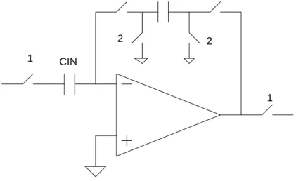
2 CONCLUSIONS3.1 Conventional Integrator
If conventional switched-capacitor (SC) structures are used to implement large time constants, the required capacitor ratios tend to be huge enough to occupy a large area thus preventing on-chip implementation. To illustrate this consider the conventional lossless integrator shown in Fig. 3-1 below [9].
CLUSIONS 1 1 2 2 VIN CIN CF VOUT
Fig. 3-1: Conventional SC lossless integrator
When the output of the integrator is taken in phase 1, the z-domain transfer function is given by . 1 1 ) ( ) ( 1 − − − = z C C z V z V F IN IN OUT (3.1)
The relationship between the time constant and clock frequency for such an integrator can be approximately given by equation (3.2).
. in CLK f C f C = τ (3.2)
If large time constants are desired, two options are available, decreasing the clock frequency or increasing the CF/CIN ratio. Decreasing the clock frequency is not really an option because we want to realize a wideband band pass function with a low pass corner at 200Hz. To prevent pre-warping errors, the clock frequency should be at least one order of magnitude larger than the low pass corner. Thus, the clock frequency is limited by the low pass corner we want to achieve. This leaves us with the option of increasing the CF/CIN ratio. The required capacitor spread can easily run into a several hundreds or even a few thousands in practice. For instance, a 1Hz high pass corner working from a 2.5 KHz clock would require a capacitor spread of around 400.
Several approaches have been investigated for realizing very large time constants in an area efficient manner. Most of these approaches achieve the required capacitor ratio as a product of two smaller capacitor ratios. For instance, if a capacitor spread of 400 can be realized as a product of two capacitor ratios of 20 each. Thus the total area has been reduced by a factor of 10 in the above case. In subsequent sections, we will discuss the various techniques by which this is achieved. For each of the techniques, we will demonstrate capacitor spread, capacitor area, the effects of op-amp DC gain and GBW, the sensitivity to capacitor mismatch, sensitivity to op-amp mismatches (differential mode offsets). We will do this for the extremes of the corner frequency, viz. 4Hz and 0.159 Hz.
3.2 Fleischer-Laker (FL) Biquad
The Fleischer-Laker biquad [8] is a wideband low-Q biquad. It consists of a two integrator loop, one lossy and one lossless. The switched-capacitor implementation is shown in Fig. 3-2 below.
1 2 1 2 2 2 1 1 2 1 C3 C4 CF1 CF2 C1 C2 OTA1 OTA2 VIN VOUT 2
Fig. 3-2: Conventional Fleischer-Laker biquad for low Q applications
The output of OTA 1 is a low pass function and the output of OTA 2 is the required wideband band pass function. The z-domain transfer function is given by
. ) 1 ( ) 1 ( 1 ) ( ) ( 1 2 1 3 2 1 2 4 2 1 1 2 1 − − − − + − + − − − = z C C C C z C C z z C C z V z V F F F F IN OUT (3.3)
To analyze approximately for the corners, the z-domain representation must be converted to an s-domain representation. This is not necessary, but since we are more
used to dealing in the continuous-time, it is more convenient. The universal transformation is given by (3.4) . 1 e sTclk z− ↔ −
TCLK is the sampling clock frequency. This is a nonlinear transformation and can lead to cumbersome expressions sometimes. If the clock frequency is sufficiently higher than the operating frequency of the SC filter, then a bi-linear transformation can be used. The transformation can be approximated by
. 5 . 0 1 1 5 . 0 1 1 5 . 0 1 5 . 0 1 2 2 2 / 1 1 CLK CLK CLK CLK CLK sT sT T s z sT sT z + ≈ + − = + − = − − (3.5)
A few more approximations are in order to derive a less cluttered expression and develop insight. . 2 4 2 1 3 2 F F F C C C C C C << (3.6)
This transformation will give us an accurate result for the high pass corner, which is low frequency, but it will give some error for the low pass corner (a large value). Using the above transformation, we obtain
(
1 0.5)
. ) 2 1 ( ) 5 . 0 1 ( ) ( ) ( 2 1 3 2 2 4 2 4 2 2 2 1 CLK F F CLK F F CLK CLK CLK F IN OUT sT C C C C T C C s C C T s sT sT C C s V s V + + + + + − = (3.7)For obtaining the high pass corner, which is at low frequency, we can make one further approximation, i.e. 1+0.5sTCLK ≈1. This will give us
. ) 2 ( 2 2 2 2 2 ) ( ) ( 2 2 4 1 3 2 2 4 4 2 4 2 1 clk F F clk F clk F in out f C C C C C f C C C s s f C C C s s V s V + + + + + − = (3.8)
In the above transfer function, the roots of the denominator (or the poles of the transfer function) will give us the approximate high pass and low pass corners. The corners can be derived as
. ) ( 2 2 ) 2 ( 2 4 1 4 4 2 2 4 4 3 2 1 4 1 4 3 2 C C passband G C f C C C C C f f C C C C C C C C f clk F LPF F clk LPF clk F HPF F clk HPF = + = ⇒ + = = ⇒ = τ ρ τ ρ (3.9)
The derived high pass corner is much more accurate than the derived low pass corner. For greater accuracy in deriving the low pass corner, we need to pre warp the low pass corner. We can thus obtain the more accurate low pass corner as in [8]
. 2 2 2 2 2 2 2 2 4 2 4 4 2 4 4 2 4 4 2 4 ⎟⎟ ⎠ ⎞ ⎜⎜ ⎝ ⎛ + = + ⎟⎟ ⎠ ⎞ ⎜⎜ ⎝ ⎛ + + = C C C Sin f C C C C C C Sin C C C f F clk F F F clk LPF ρ (3.10)
Thus, the problem of realizing the large time constant has been solved by now involving four capacitors rather than just two in conventional switched-capacitor structures. From the above equations a few facts are clear:
1. C4 < CF2 because the clock is one order higher than the low pass corner 2. C4 and CF1 are much larger than C2, C3 for large time constants
3. C1 is as large as C4 if a gain of 1 is desired and larger for larger gains
3.2.1 Capacitors, matching and sensitivity
C4, C2, C1 and CF2 must be mutually matched, as must C3 and CF1. Since C2 and C3 are the only small capacitors in their respective cluster, both can be unit capacitors for common centroid matching to be possible. The capacitor values are given in Table 3-1. The low pass corner is always fixed at 200Hz. The values have been optimized for spread. They can also be optimized for GBW as will become clear in the discussion in section 3.2.3.
Table 3-1: Capacitor values for FL biquad of Fig. 3-2
fHPF C1 C2 C3 C4 CF1 CF2
0.159 Hz 36 1 1 36 70 70
4 Hz 8 1 1 8 14 14
The capacitor spreads depend on both the high pass and the low pass corner. While having a small high pass corner causes a large capacitor spread, the presence of a low pass corner pushes the spreads to even higher values. This is one disadvantage of this biquad.
The sensitivities with respect to all capacitor mismatches have a magnitude of 1. As an example for calculation, let us calculate the sensitivity of the high pass corner with respect of CF1. . 1 1 1 1 ⎟⎟÷ =− ⎠ ⎞ ⎜⎜ ⎝ ⎛ ∂ ∂ = F HPF F HPF C C C S HPF F ρ ρ ρ (3.11)
Similarly it can be shown that the sensitivity with respect to C2 and C3 is 1 while the sensitivity of the high pass corner with respect to C4 is -1. Thus the absolute value of sensitivity with respect to all capacitors is 1. The absolute sensitivity is given by
. 4 4 3 2 ! 1 + + + = = HPF hpf HPF HPF F C C C C S S S S S ρ ρ ρ ρ (3.12)
3.2.2 Effects of finite DC gain
The ideal transfer function in a Fleischer-Laker biquad has a zero at the origin and two left half poles in the s-plane for a continuous time implementation. For a discrete time implementation, the zero ideally lies on the unit circle and the poles lie within the unit circle of the z-plane. This is true if the op-amps are ideal. However, if the op-amp is not ideal, then the transfer function contains a zero inside the unit circle (analogous to a left half zero). This causes not only a phase error, but also an error in the 3-dB high pass corner. The main reason for this zero is that a lossless integrator if implemented by a non-ideal op-amp is actually lossy. The larger the gain of the op-amp, the smaller the loss. The transfer function considering finite DC gain is given by
(
)
(
)
(
)
(
)(
)
. 1 1 ) 1 ( 1 1 1 ) 1 ( 1 ) 1 ( ) ( 1 2 1 1 2 1 3 2 2 1 1 3 2 2 1 2 4 1 2 / 1 2 1 1 2 1 1 1 3 1 1 2 2 1 − − − − − − − + + = + + + + = + − + − + + − + + − = A A C C C C G A C C A C C C C G z G z G z C A C z A C C z H F F F F F F F (3.13)The frequency of the zero is given by
. 1 1 3 F clk Z C A C f = ρ (3.14)
For small DC gains, this zero can be uncomfortably close to the required high pass corner. For instance, in the biquad above, if OTA 1 has a DC gain of 40 dB (normal for a current mirror OTA), then the zero frequency is only three times lower than the frequency of the required pole. By increasing the spread, the zero can be pushed to lower frequencies, but the spreads are already too high. Thus, OTA 1 must have a large DC gain. A typical folded-cascode (gain = 74 dB) can push the zero to reasonably lower frequencies, so that it does not affect the response too much.
Another error is due to the apparent change in the values of CF1, CF2 and C4. This change is entirely due to the DC gain. The apparent values become
(3.15) ). 1 ( ) 1 ( ) 1 ( 1 2 4 4 1 2 2 2 1 1 1 1 − − − + → + → + → A C C A C C A C C F F F F
These errors are quite obvious from inspection. These errors are quite small however. The point that we are trying to make here is that one has to use large DC gain
to realize the required transfer function with a reasonable accuracy. These conclusions can be verified via simulations.
3.2.3 Op-amp GBW
OTA 1 is effectively loaded by capacitor C3 during phase 1 and C2 during phase 2. Both of these are small capacitors and hence OTA 1 has minimal GBW requirements. OTA 2 however is loaded by a parallel combination of C1, C2 and C3 during phase 2. The loading diagrams for OTA 2 are shown below in Fig. 3-3a and Fig. 3-3b.
C3
C2 C1
CF2 C4
CL
Fig. 3-3a: Loading configuration for OTA 2 of Fig. 3-2 during phase 2
C1+C2 VIN
VOUT
CL+C3 CF2+C4
The loop GBW is given by . 1 ) ( _ 4 2 2 1 3 2 1 ⎟⎟ ⎠ ⎞ ⎜⎜ ⎝ ⎛ + + + + + + = C C C C C C C C g GBW loop F L m (3.16)
C1 is a big capacitor and loads the OTA, impacting settling time. Thus, as the time constants increase and push up the spread, C1 increases and thus OTA 2 requires greater power consumption (gm) for proper settling.
3.2.4 Op-amp offsets
One advantage of the Fleischer-Laker biquad is that it is robust with respect to op-amp offsets. This is why, in single ended implementations of large time constants, the FL biquad is preferred over other methods. For differential ended structures, this advantage vanishes because of the very nature of differential ended circuitry. In differential ended circuits, the biasing offsets (systematic offsets) appear as a common mode voltage, which is eliminated by the common mode feedback circuitry. Mismatch offsets (random offsets) can be eliminated by chopper stabilization. The output offset of the FL biquad is approximately equal to (but of opposite sign) the input referred offset of the OTA 1. This can be intuitively seen by understanding that in steady state, no charge flows through either integrating capacitor CF1 or CF2. Thus,
(3.17)
.
1 , , ,off inoff OTA
out V
3.3 The T-Cell Method [4]
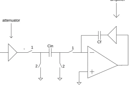
To understand the T-Cell method, consider the discrete time integrator in Fig. 3-4. To achieve a large time constant CIN needs to be as small as possible and CF should be as large as possible. Conceptually, this can be achieved by placing an attenuator between the input and CIN and/or an amplifier between the output and CF. The conceptual schematic is shown below in Fig. 3-4.
Vin Vout 1 1 2 2 Cin Cf ˜ attenuator amplifier
Fig. 3-4: Conceptual implementation of large integrator time constants
Thus the input signal is reduced by an attenuating factor (>1) and the feedback signal is increased by the amplification factor (>1). Thus, the time constant of the integrator increases by the product of the attenuation and amplification factors. The effect is equivalent to reducing the input capacitor, Cin (increasing the resistor) and increasing the feedback capacitor CF (the integrating capacitor). Amplification can be implemented only by adding an extra OTA. This increases power consumption.
Attenuation does not need active elements. Passive voltage division can implement it. This is the theory behind the T-Cell implementation. The T-Cell method implements a small input capacitor by means of capacitive (switched capacitive) voltage division. The switched-capacitor implementation of the T-Cell integrator is shown in Fig. 3-5.
C1 C2 1 2 2 1 2 CIN CF VIN VOUT
Fig. 3-5: Large TC integrator using the T-Cell technique
C1 and C2 make sure that only a small fraction of the input charge is actually integrated by passage through CF. The z-domain transfer function, when the output is sampled in phase 1 is given by
. 1 1 ) ( ) ( 1 2 1 1 − − + + − = z C C C C C C z V z V F IN IN in O (3.18)
To implement a lossy integrator using the T-Cell, one will have to use it in the Fleischer-Laker biquad. This structure is not parasitic-insensitive. When using poly
capacitors, the bottom plate parasitic capacitor could be as large as 20% of the main capacitor. Metal-Metal capacitors have smaller parasitic effects, but they occupy a huge amount of chip area compared to poly capacitors. Therefore, we will not be using this structure or discussing it further.
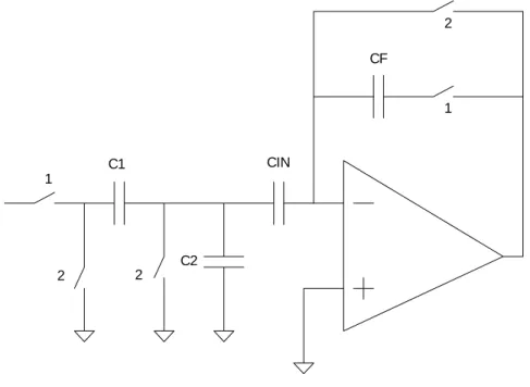
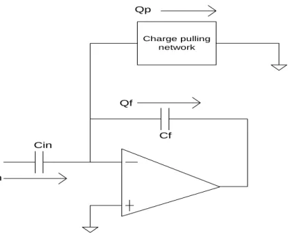
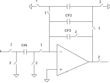
3.4 The Split-Integrating Capacitor Technique [3]
Consider the lossless integrator again. The T-Cell technique was concerned with making the input capacitor look small. The split-integrator technique uses the same principle, but the implementation is parasitic-insensitive. The way it does this is by throwing away a big fraction of the input charge and only passing a small fraction of it through the feedback integrating capacitor. The conceptual diagram is shown in Fig. 3-6.
Qin Qf Cin Cf Charge pulling network Qp
In the conventional integrator, the whole of the input charge passes through the integrating feedback capacitor. In the split-integrating technique, a considerable fraction of the input charge is sucked in by the charge pulling network and only a small fraction of the input charge passes through the integrating feedback capacitor. This operation makes the feedback capacitor look much larger than it actually is or conversely, we can say that it makes the input capacitor look small.
Fig. 3-7 demonstrates the discrete time implementation of the technique. The feedback capacitor CF is split into three capacitors, CF1, CF2 and CF3. The circuit exploits an extra op-amp phase. In the conventional integrator, the integration and sampling are performed only in phase 1. In phase 2, the op-amp is idle and the output is a don’t care. In the split-integrator technique, both phases are used. In phase 1, the input charge (Qin = CinVin) is divided between CF1 and CF2. In phase 2, the bigger capacitor, CF1 discharges to ground, and a significant portion of the input charge is lost. The smaller capacitor, CF2, which holds only a small portion of the input charge, discharges through the integrating capacitor. Thus only a small portion of the input charge is integrated, making the integrating capacitor look really very big.
1 1 2 2 2 1 1 2 2 2 CF1 CF2 CF3 VIN CIN VOUT
Fig. 3-7: SC implementation of the concept shown in Fig. 3-6
The z-domain transfer function can be written as
. 1 ) ( ) ( 1 2 / 1 1 2 3 2 − − − + − = z z C C C C C z V z V CF F IN F F in out (3.19)
The relationship between the time constant and the clock frequency is given by
. 1 2 1 2 3 clk F F F IN F f C C C C C + = τ (3.20)
Thus for a large time constant, CF3 and CF1must be large while CIN and CF2 must be small. Also CIN, CF2, CF1, CF3 must all be mutually matched.
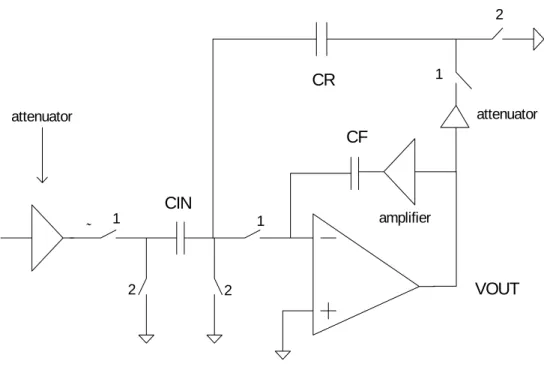
Now, we must, at this point, begin to wonder whether a lossy integrator can be synthesized using this technique. It may be impossible to do this using only one op-amp. To implement a lossy integrator, let us go back to the conceptual diagram as given below.
1 1 2 2 ˜ attenuator amplifier 1 2 attenuator VIN CIN CR CF VOUT
Fig. 3-8: Conceptual implementation of large TC LPF
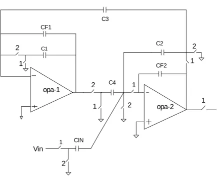
The technique makes the input capacitor CIN look small (using the attenuator). To maintain gain and also a large time constant, it must also make CR look small. To do this, it must attenuate the output VOUT(n). Both clock phases are already utilized (one is utilized in attenuating the input signal and the other in the integration). So we would need an extra clock to make CR look small. Thus, we cannot implement a lossy integrator, using just this one op-amp and only two clock phases. To implement a lossy integrator using this technique and only two clock phases, we will need to use this integrator in an FL biquad. The discrete-time implementation is shown in Fig. 3-9. The loop implements a high pass function. Technically, we don’t need CF2. I have just included it for completeness. We can allow the value of CF2 to be any value of our choosing, i.e. any arbitrarily small value.
OTA1 OTA2 C1 CF2 C2 C5 C4 C3 CF1 1 2 1 2 1 2 1 2 1 2 1 1 2 2 VIN CIN VOUT
Fig. 3-9: A large time constant integrator in the FL biquad
The transfer function is given by
(
) (
)
. ) ( 1 1 1 ) ( 1 4 3 2 1 5 3 1 2 2 1 2 1 1 2 − − − − + + − + − − − = z C C C C C C C C C z z z C C z H F F F F IN (3.21)The high pass corner is then given by
(
3 4)
. 2 1 5 3 1 C C C C C C C f F clk HPF + = ρ (3.22)If C1=C3=C5 = C, and CF1 = C2 = Cβ, and C4 = (β-1) C, then the corner is given by equation (3.23). . 3 β ρ clk HPF f = (3.23)
3.4.2 Capacitors, matching and sensitivity
C5, C3, C4, CF1 form one cluster. C1, Cin, Cf2 and C2 form another cluster. The various capacitor sizes are given in Table 3-2.
Table 3-2: Capacitor values for Fig. 3-9, DNM stands for does not matter
Corner C1 C2 C3 C4 C5 CIN CF1 CF2
4 Hz 1 4 2 8 2 4 5 DNM
0.159 1 14 2 26 2 14 26 DNM
The magnitude of sensitivity of the high pass corner with respect to all capacitor ratios is 1. Sensitivity is defined the same way as in section 3.2.1. However, the structure is more sensitive that first order sections or even the conventional FL biquad, because there are more ratios (3 rather than 2) involved in determining the time constant. The value of total sensitivity (as defined in B1) is 6.
3.4.3 Op-amp DC gain
If the finite DC gain of the op-amp is considered, the transfer function is given by equation 3.24 below.
(
) (
)
. ) ( ) 1 ( 1 1 ) 1 ( 1 ) ( 4 3 2 1 5 3 1 1 2 2 2 2 1 1 3 1 2 1 1 1 3 1 2 C C C C C C C G Gz C A C C C A C C z z A C C z C C z H F F F IN F F F F IN + = + ⎟⎟ ⎠ ⎞ ⎜⎜ ⎝ ⎛ + + + − + − + + − − = − − − − (3.24)Just like in the conventional FL biquad, the finite DC gain of OTA moves a zero within the unit circle. The frequency of this zero is given by
. ) 1 ( 1 3 + = A C C F z ρ (3.25)
For small gains of OTA 1, the zero is too close to the high pass corner.
3.4.4 Op-amp GBW
OTA 1 is loaded by the parallel combination of C5 and C1 while OTA 2 is loaded by the parallel combination of Cin, C1 and C3. All of these are small capacitors and hence there will not be much of a problem with respect to settling even for minimum power consumption.
3.4.5 Op-amp offsets
The output offset of this biquad can be shown to be equal in magnitude to the input referred offset of OTA 1. So offsets are not a problem in this biquad.
3.5 The Nagaraj Technique [5]
The Nagaraj technique is by far the most area efficient method of implementing large time constants yet. A circuit schematic of the Nagaraj integrator is shown in Fig. 3-10.
VIN 1 2 CIN CF 2 1 CR 2 VOUT 2
Fig. 3-10: The Nagaraj integrator
In each of the schemes discussed earlier, the basic trick has been the same. The charge passing through the integrating capacitor must be limited to as small a fraction of the input charge as possible. The Nagaraj technique is no different in this respect. However, in the techniques discussed above, attenuation and integration were performed by different capacitors. In the Nagaraj technique, the same capacitor is used to perform the integration as well as the attenuation function resulting an almost 50% saving in total capacitance. In the above circuit schematic, capacitor C2 is used for attenuation as well as for integration. This is illustrated by Fig. 3-11.
The circuit on the left illustrates the charge transfer in phase 1 while that on the right illustrates the charge transfer in phase 2. In phase 1, the entire input charge (QIN = QF) flows through CF, which is the big integrating capacitor. In phase 2, almost the entire
CIN CF CR QIN QF-QR QR CIN CF QIN QF
Fig. 3-11: Illustrating the integrating principle in the Nagaraj integrator
input charge (QIN-QR) flows through the integrating capacitor, but in the reverse direction. Thus, in effect, only a small portion of the input charge (QR) is integrated by the large capacitor CF. Voltage waveforms are shown in Fig. 3-12.
During phase 1, the output voltage takes a step of a certain size in the negative direction. This is when the input charge flows through CF. During phase 2, when a large fraction of the input charge is returned by CF, the voltage waveform takes a step in the positive direction. The step in the positive direction is a little less than the one in the negative direction. PHASE 2 VOUT(n-1) PHASE 2 VOUT(n) PHASE 1 VOUT(n-1/2)
Fig. 3-12: Illustrating the voltage waveforms in the Nagaraj integrator
The z-domain transfer function of the integrator is
. 1 1 1 ) ( 1 2 / 1 2 2 − − − + − = z z C C C C C C z H F IN F F (3.25)
The time constant of the integrator is given by
. 1 1 2 2 clk F IN F F C f C C C C C ⎥ ⎦ ⎤ ⎢ ⎣ ⎡ + = τ (3.26)
Thus CF is a large capacitor and CIN, C2 are small capacitors. Rather large time constants can be implemented with reasonable capacitor ratios.
The idea above can be extended to realize lossy integrators as shown in Fig. 3-13. The transfer function of the integrator can be shown to be
. 1 1 1 1 1 1 1 ) ( 1 2 2 1 2 1 1 2 / 1 2 1 2 ⎥ ⎥ ⎥ ⎥ ⎥ ⎥ ⎥ ⎦ ⎤ ⎢ ⎢ ⎢ ⎢ ⎢ ⎢ ⎢ ⎣ ⎡ ⎟⎟ ⎠ ⎞ ⎜⎜ ⎝ ⎛ + ⎟⎟ ⎠ ⎞ ⎜⎜ ⎝ ⎛ + + − ⎟⎟ ⎠ ⎞ ⎜⎜ ⎝ ⎛ + ⎟⎟ ⎠ ⎞ ⎜⎜ ⎝ ⎛ + − = − − − z C C C C C C C z z C C C C C C C C z H F F F F F IN F F (3.27)
The DC gain of this lossy integrator (LPF) is equal to CIN/C1.
VIN VOUT CIN CF C2 C1 1 2 1 2 1 2 2
The corner frequency is given by . 1 1 1 2 1 2 2 1 ⎟⎟ ⎠ ⎞ ⎜⎜ ⎝ ⎛ + ⎟⎟ ⎠ ⎞ ⎜⎜ ⎝ ⎛ + = F F clk F C C C C f C C C ρ
(3.28)
Large time constants are obtained by keeping CF large and C1, C2, CIN small. Let us now analyze the Nagaraj low pass filter for various parameters.
3.5.2 Capacitors, matching and sensitivity
Capacitors C1, C2, Cin and CF belong to the same cluster and hence must be mutually matched. Since C1,2,in are all small capacitors, all three of them cannot be mutually matched and be unit capacitors at the same time. Here, we come across a tradeoff between capacitor spread and capacitor area. Given in Table 3-3 is the list of capacitor values optimizing spread. Table 3-4 optimizes area.
Table 3-3: Capacitor values for Fig. 3-13 optimizing spread
Corner CIN C1 C2 CF
0.159 2 2 2 98
Table 3-4: Capacitor values for Fig. 3-13 optimizing area
Corner CIN C1 C2 CF
0.159 2 2 1 70
4 2 2 1 13
The sensitivities are given by
(3.29) . 4 1 1 2 2 1 = = = − = S S S S HPF HPF HPF F C C C ρ ρ ρ
The Nagaraj structure is about as sensitive as the conventional Fleischer-Laker biquad.
3.5.3 Op-amp DC gain
If op-amp DC gain is taken into account, the transfer function for the low-pass filter can be derived to equal the expression in equation (3.30).
. 1 1 1 1 1 1 1 1 ) ( 1 1 1 2 2 2 1 1 2 2 2 ⎟ ⎟ ⎟ ⎟ ⎟ ⎟ ⎟ ⎟ ⎟ ⎟ ⎟ ⎟ ⎠ ⎞ ⎜ ⎜ ⎜ ⎜ ⎜ ⎜ ⎜ ⎜ ⎜ ⎜ ⎜ ⎜ ⎝ ⎛ − ⎟ ⎟ ⎟ ⎟ ⎟ ⎠ ⎞ ⎜ ⎜ ⎜ ⎜ ⎜ ⎝ ⎛ ⎟ ⎟ ⎟ ⎟ ⎟ ⎠ ⎞ ⎜ ⎜ ⎜ ⎜ ⎜ ⎝ ⎛ + ⎟⎟ ⎠ ⎞ ⎜⎜ ⎝ ⎛ + ⎟⎟ ⎠ ⎞ ⎜⎜ ⎝ ⎛ + − ⎟⎟ ⎠ ⎞ ⎜⎜ ⎝ ⎛ + ⎟⎟ ⎠ ⎞ ⎜⎜ ⎝ ⎛ + − = − z AC C C C C C C C C C C C C C C C z H F F F F F F F IN (3.30) The new corner frequency is given by
. 1 1 1 1 2 1 2 2 1 ⎟ ⎟ ⎟ ⎟ ⎟ ⎠ ⎞ ⎜ ⎜ ⎜ ⎜ ⎜ ⎝ ⎛ + ⎟⎟ ⎠ ⎞ ⎜⎜ ⎝ ⎛ + ⎟⎟ ⎠ ⎞ ⎜⎜ ⎝ ⎛ + = F F F F clk AC C C C C C C C C f ρ (3.31)
The error in the time constant is thus given by
. 2 1 1 A C C C C F = ε (3.32)
If CIN = C1 = C2 = C and CF = βC, then the error is given by
. A β
ε = (3.33)
Thus for a time constant of 1s (cutoff of 0.159 Hz) and a clock of 2.5 KHz, the Spread required is 50 and the DC gain required for 1% error would be 5000 or 74dB.
3.5.4 Op-amp GBW
There is not much stress on the GBW of the OTA because the AC loading capacitor in both phases is CIN, which is a small capacitor. The GBW requirement can be met easily by the minimum power OTA (40nA).
3.5.5 Op-amp offsets
The effects of the op-amp offsets can be derived in straightforward manner. The way to do this, is to set the input to zero, assume infinite DC gain and assign an input referred offset of VIN,off,OTA to the OTA. The output offset can be derived to be
. 2 , ,
,off inoffOTA
out V
V = β (3.34)
Since we are using fully differential configurations, we do not worry about biasing offsets. Mismatch offsets can be removed by chopper stabilization [10].
3.6. Combining the FL Biquad with the Nagaraj Integrator
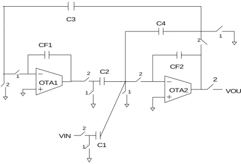
We might recall that the FL biquad contained a two integrator loop of which one integrator was lossy and the other, lossless. Two of the problems, viz. large capacitor spread and area, and loading effect can be greatly alleviated, by replacing the conventional integrator with the Nagaraj integrator. Doing so reduces the area as well as the spread as compared with the first order Nagaraj lossy integrator. The switched-capacitor implementation of the improved FL biquad is shown in Fig. 3-14.
opa-1 opa-2 C1 C3 C4 Vin Vout 1 2 2 1 2 1 1 2 2 1 1 C2 CIN CF2 CF1
Fig. 3-14: FL biquad using the Nagaraj integrator
Opa-1 implements the lossless Nagaraj integrator while opa-2 implements the conventional lossy integrator. Recall that in the conventional FL biquad, CIN, Cf2 and C2 would be large capacitors increasing the area as well as the loading on opa-2. In this improved biquad, the sizes of CIN, C2 and Cf2 can be drastically reduced because the large time constant is chiefly being realized by the capacitors C1, C3 and Cf1. This is well illustrated by the transfer function that is written below as
(
) (
)
. 1 1 1 1 ) ( 1 1 1 2 2 1 4 3 1 2 2 1 2 1 1 2 − − − − ⎟⎟ ⎠ ⎞ ⎜⎜ ⎝ ⎛ + + − + − − − = z C C C C C C C C C z z z C C z H F F F F F IN (3.35). 1 ) ( 1 2 1 2 4 3 1 2 2 2 2 2 ⎟⎟ ⎠ ⎞ ⎜⎜ ⎝ ⎛ + + + ⎟⎟ ⎠ ⎞ ⎜⎜ ⎝ ⎛ − = F F F clk F clk F in clk C C C C C C C f C C f s s C C f s s H (3.36)
The roots of the denominator will give us the respective corner. Our concern is with the high pass corner. The high pass corner is given by
. 1 1 1 2 1 2 4 3 1 ⎟⎟ ⎠ ⎞ ⎜⎜ ⎝ ⎛ + = F F clk HPF C C C C C C C f ρ (3.37)
And the corresponding time constant is given by
. 1 1 1 4 3 1 2 1 2 ⎟⎟ ⎠ ⎞ ⎜⎜ ⎝ ⎛ + = F F C C C C C C C τ (3.38)
Thus the time constant here is a ratio of three transistors. Thus the loading effect on OTA 2 can be reduced in comparison with the conventional Fleischer-Laker structure. Further, lower spreads can be achieved because now three ratios are involved. The low pass corner is given by
. 2 2 F clk LPF C C f = ρ (3.39)
Both C2 and CF2 can be small capacitors.
3.6.2 Capacitors, matching and sensitivity
If we optimize for spread, Table 3-5 gives the values of the capacitors in numbers of unit capacitors.
Table 3-5: Capacitor values for Fig. 3-14 optimizing spread
Corner C1 C2 C3 C4 CIN CF1 CF2
.159 Hz 2 12 2 1 12 28 18
4 Hz 2 4 2 1 4 10 6
Thus, this structure does a better job of reducing spread and area than the Nagaraj integrators. However, for large time constants, OTA 2 might be loaded by CIN. Thus, we can optimize loading for 0.159 Hz using the values of capacitors as given in Table 3-6.
Table 3-6: Capacitor values for Fig. 3-14 optimizing loading on opa-2
Corner C1 C2 C3 C4 CIN CF1 CF2
0.159 Hz 2 2 2 2 2 100 3
Note that if we eliminate Cf2, we get a one-integrator loop with two OTAs. The structure will be a pure high pass. This is not a problem if a stand-alone high pass is required or if the succeeding stage is available to implement a low pass. Thus, we may be able to reduce the area by eliminating CF2. If we eliminate CF2, the low pass corner is not defined. It is set by the OTA bandwidth. However, to define the low pass corner, we can have another low pass block following this stage.