Abstract
The actual idea of a telephony structure shows a Private Automatic Branch Exchange (PABX) directly controlling a whole
communication system. Ringing and caller identification signals,
voltage setting for the phone sets among other important parameters all are transmitted using twisted pair cables that have to be installed and distributed along the building. The use of existing indoor power lines as the communication channel
benefits the installation of the telephony system because the network infrastructure is already mounted. However,
power lines behave noisy and aggressive when transmitting high frequency signals and in order to establish effective
communication, modern modulation and transmissions schemes have to be implemented. With this new conception,
the transmission scenario changes completely and so does the system. This paper presents the idea for the design of an analog modular electronic interface that is intended to create a sort of correlation between the current standards for conventional
communication schemes and this system, which uses power
lines to communicate between its peers.
Key Words
Power Line Communications, Multi-Carrier Code Division Multiple Access, Private Automatic Branch Exchange.
I. Introduction
With the explosion of power lines communication that has been taking place recently people around the world research unsparingly to take advantage of this technology. The telephony system that is being implemented here uses existing power lines of an indoor establishment to communicate between its users as a way to decrement the prices of the design since there is no need of mounting the network. In this paper we describe the challenges ahead of the technology change as well as the solution approach in order to implement the system. The system
overview, the transmission scheme to use, the way the PABX communicates with the users, how to interface to the Public System Telephony Network (PSTN), the way the ring signal is generated, the implementation of the caller identification
feature and how to interface to the standards existing phone sets available in the market are some of the issues that are treated in this paper.
II. System Overview
The main characteristics of this system are its low cost when compared with existing large telephone systems and the
reliability, flexibility and ease of operation. The system can be divided in two major elements: the first element is a Peripheral Component Interconnected (PCIPABX) module, designed for
installation in a PCI slot of a PC. It includes an analog unit to
interface with the (PSTN) and a Signal Processing Module, which will perform all the features of a standard switchboard, plus other specific functions such as caller identification, call waiting, call transfer, automatic interactive voice interface, multiple-user account setting, automatic multiple-user billing and music on hold
among others; The other element is a multifunction power
line-to-phone set transceiver which, by design, will allow the
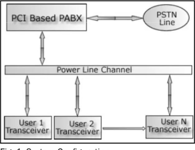
standard digital phone sets available in the market to interface with the PABX board. The PABX board communicates with each user so each user must have a user phone set transceiver
board. Fig. 1, shows the system configuration: Power lines were
designed to carry high voltage levels at low frequency rates. It becomes a very harsh scenario when transmitting low power high frequency signals. The signal is subject to all kind of noise and interference and a large attenuation is observed as the
distance of the line increases. A multi-path environment due
to the amount of branches already connected in the network
and open taps produce signal reflections and attenuations
notch which can be clearly seen in the frequency response of
the channel [7, 8, 14].
Fig. 1: System Configuration
III. Selecting the Transmission Scheme
The impedance of the channel is not constant and varies
approximately from 20 to 500 Ohms [8, 14] depending on the frequency, the length of the path, the amount of paths and the
number and type of loads connected to the network at a given time even though for this latest issue load characterization is
possible using neural networks and statistical methods [9].
Induction motors and switching power supplies among others are noxious sources of noise that can damage considerably any signal transmitted at a different frequency than the one of
the mains [5, 11]. Orthogonal Frequency Division Multiplexing (OFDM) and particularly in this case Multi-Carrier Code Division Multiple Access (MC-CDMA) are broadband transmission
schemes which due to their characteristics behave highly resistant to the most of the challenges exposed above that
exist in power lines [3-4, 6]. In this type of transmissions several sub-carriers are employed to transport the user’s
data stream signal and each carrier signal is spread in the
bandwidth spectrum by using a pseudo-code or pseudo-noise (PN) pulse train. Either OFDM or MC-CDMA offers a suitable
solution for transmitting information across power lines. The
use of MC-CDMA specifically for this project is justified due to that OFDM applies coding to evade an excessive Bit Error Rate (BER) on sub-carriers that are in a deep fade., thus the number of needed sub-carriers is larger than the number of bits or symbols transmitted simultaneously. MC-CDMA replaces this
Implementation using Power Line Communications in
Telephone System
1
Pradeep Kumar Jaisal,
2Pankaj Kumar Mishra
encoder by an N x N matrix operation. In other words MC-CDMA
offers better frequency diversity to combat frequency selective
fading, one of the main issues seen in power lines.
IV. Interfacing with the PSTN
There are some important parameters to know before start
interfacing the PCI-PABX board with the PSTN. First, the needs
of a standard RJ11 connector present to connect with the PSTN
line. The voltage, once connected to the line is approximately equal to 48 Volts DC. When a call takes place a ring signal is
generated from the central. The ring signal is approximately
90 Vpp at a very low frequency of around 30 Hz. If the call is attended and an “off-hook” detected by the central the voltage is then set to a low value of around 9 to 12 volts DC for standard
phone sets. The standard phone set has an internal impedance
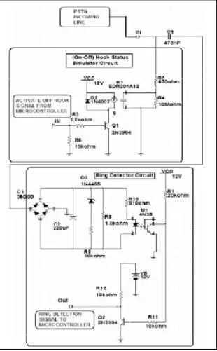
at “off hook” stage of approximately 600 Ohms and a very high impedance when it is “on hook.”[2]. The circuit showed in fig. 2, guarantees a standard interface with the PSTN.
Fig. 2: Ring Detector and off look simmlator circuit
The phone ring detector block detects whenever there is an incoming ring signal from the PSTN and generates a pulse train
at a high frequency, which will be detected by the microcontroller
onboard. A pulse train prevents the microcontroller from being activating with a simple noise pulse. The microcontroller
executes a verification procedure to ensure an effective ring detection signal and activates the input of the “on/off hook”
stator simulator module which basically bridges the high
resistance R4 in the voltage divider leaving just R5, the 600 Ohms resistance connected in the circuit; in other words, it
simulates a change of status from on hook to off hook so that the central perceives the current change and establishes the communication.
V. Coupling to the Power Line Network
There are two main choices for signal coupling to the power
lines line to neutral (Differential Mode) and neutral to earth protection wire (Common Mode) [13]. This second method
is usually less noisy and the attenuation of the signal is also smaller but may be dangerous when implementing due to the neutral wire and the line combined together. Proper safety measurements are to be carried out in order to implement this second one and many countries do not allow it because of their rules and regulations over the electrical power systems. The Toroidal ferrite core transformer commonly used for power line coupling for low frequencies becomes problematic and causes the signal degradation when transmitting and receiving high
frequency signals. Fig. 3, shows a suitable solution for the design of the ferrite core [1].
Fig. 3: The Coupling Transformer Ferrite Core
Fig. 4, shows the coupling network. A protection bridge network
composed by Schottky diodes is placed in the circuit to prevent noise damage the circuit. The two suppressor diodes ensure
that the four Schottky diodes are always reverse-biased for
all signal amplitude to be transmitted. The characteristic
impedance in power lines at frequencies of interest, in this case from about 20 MHz to 30 MHz, will vary between 20 and
500 Ohms approximately. Capacitors C1 and C2 must have
the same value from 47 nF to 68 nF to approximately match
the average power line impedance. The resultant impedance will be the resultant one from the combination between the Inductance of the primary winding or main side winding of the transformer and the capacitive reactance produced by the capacitors placed in the main side.
Fig. 4: The coupling Network
In this circuit, the receiver and the transmitter have been
conceived together looking forward to minimize the size of
the final circuit boar for both, the PCI based PABX as well as the
phone set transceiver. The implementation of the transformer
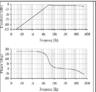
is a result of the coupling network proposed in [1]. The coupling network was also simulated with Multisim 7 obtaining the graph of the frequency response shown in fig. 5.
Fig. 5: Power line Couping Frequency Response Attenuation values are perfectly appropriated for the
frequency band from 100 KHz to 30 MHz.
VI. Transmitting Ring Signals over the System
Ring signals are low frequency and high amplitude signals and can not be transmitted by any circumstance through the power line channel where the mains have similar characteristics. This type of signals which in this present design can not be transmitted through the communication channel are simply generated locally at the level of the receiver either the PCI based PABX board or the user interface transceiver board. The information is 202 preliminarily transmitted as data inserted in the modulation scheme and it is recognized and processed by the receiver in order to generate the ring signal. The ring waveform is generated by hardware in this design; however the
ring cadence is controlled by the microcontroller. Fig. 6, shows
the ring generator circuit and its operation.
Fig. 6: Ring Generator Circuit
The Wien-Bridge sine wave oscillator generates the waveform, which is later amplified by the operational amplifier and the
transformer. This transformer has special characteristics to
work at a low frequency rate, approximately 30 Hz. The ring cadence, as stated before, is directed by the microcontroller and has an “on” duration of three second and “off” duration of four
second. The pulse enables or disables the output signal of the
oscillator by means of a bidirectional analog key LM4066.
VII. Interfacing with the User Phone Set
The on-off hook detector and the user phone set voltage settings
circuit will detect whenever the user pick up the phone either when the phone is ringing or the user just want to initiate a
call. The 1.8 KΩ resistor connected in series with the line will
drop the line voltage to about 12 volts whenever the phone set becomes off hook and the current starts to circulate through it.
The voltage comparator LM311M identifies an off hook status
in the phone producing a 12 volts output signal when the phone is off hook and zero in the opposite case to be sent to the
microcontroller as showed in fig. 7.
Fig. 7: User Phone Set on off Hook status Simulator
The loop current is around 75 μA or lower when the phone is on
hook. Whenever the user picks up the phone the loop current will increase up to 70 mA maximum and the current sensor
identifies the off hook status of the Phone. When an off hook
status is detected 12 volts is set at the microcontroller input.
VIII. The DTMF and Caller Identification signals
DTMF stands for “Dual Tone Multi Frequency”. This method represents digits with tone frequencies, in order to transmit
them over an analog communications network. In telephone
networks, DTMF signals are used to encode dial trains and other information. For DTMF encoding, the digits from 0 to 9 and the characters from A to D, and */E and #/F are combinations of
two frequencies:
All DTMF signal frequencies as it can be observed in Table 1
are inside the voice spectrum and thus may be 203 transmitted through the power line channel. However the PCI based PABX is to be equipped with transceiver for information processing
and billing. For example, when a user picks up the phone to place a call, the user transceiver board links the PABX, which replies sending a dial tone. The user dials a number so DTMF
audio signals are sent over the power lines and need to be
identified and processed by the PABX in order to establish the
solicited communication. All records are stored in a database for further billing processing. Something similar occurs with caller
identification signals. The caller ID information is transmitted using a frequency shift keyed (FSK) modem, it uses 1200 Hz for logic 1 “Mark” and 2200 Hz for logic 0 “Space”. These tones
are used to transmit short messages in American Standard Code for Information Interchange (ASCII) character code
form. The transmission of message occurs between the first
and the second ringing signal. The information sent includes
the date, time, and calling number. The caller identification signal may be generated two ways, either using one of the existing commercial IC’s and inserting this in the hardware configuration, or just generate it as part of the controlling software of the microcontroller. In order to minimize cost, which is one of our premises for this design, the caller ID signal
generation is conceived as part of the software designed for
the microcontroller. The use of Virtual Peripheral Concept (VPC) when programming, optimizes the execution performance of
the microcontroller allowing it to achieve complicated tasks
like this CID generation with a high grade of reliability. The PCI based PABX board needs both, a Caller ID generator and also
a detector because of the link with the incoming PSTN line.
IX. The Economic Analysis
Based on research done on PBX system manufactures and
vendors websites, the costs of standard wired PBX systems typically range from about $500 to $2,000 per user, depending
on the features and functionality included in the PBX system.
Table 2 shows a typical cost [16] of the average PBX systems
installations.
Table 2: Typical costs for wired PBX system
The purchase and the installation of the system is approximately
$50,000, for a PBX with a capacity for 40 users. A real
alternative that allows small companies to avoid spending this huge amount of money is the use of small wireless PBX
systems [15]. This is usually a less expensive alternative but
the majority of the manufacturers that build these systems
produce them for a reduced number of users, usually from 4 to 16 users. Prices for these systems range between $250 and $500 per user connected, including the system and the
installation. These systems usually require the use of specific phone sets, also provided by the manufacturer, but their prices
are higher than the conventional phone set prices available in
the market, including those that use wireless technology. The
system proposed in this paper is aimed to reduce the production cost and the installation cost. The costs range between $100 and $300 per user including the price for the PBX and Central
Computer. These figures are less than the wired systems and
relatively cheaper than the wireless PBX systems. This system has a lower cost compared with the wireless systems because of the possibility of using the existing phone sets which are normally cheap and easily accessible in the market. The main drawback of the power line based PBX compared with the
wireless PBX, is the lack of mobility that wireless systems
usually provide to users. Using standard wireless phone sets this system can also provide similar mobility to wireless PBX systems.
X. Conclusion
The change from twisted pair standard cables of telephony systems to the use of power lines as the communication channel offers an advantageous scenario to decrease installation cost. With the technology change new challenges come into sight. A solution approach was suggested in this paper to overcome these issues. Future upgrade for data transmission
up to 10 Mbps is also possible with this system. The DTMF transceiver on the PCI-PABX board may also be implemented using the Virtual Peripheral concept of programming for the
microcontroller software; this also reduces the overall cost of the system. The favorable communication schemes make data transmission effectively possible facilitating the future development of complex data networks and data acquisition
systems communicating through the power lines, not only for
Internet and data transmission but for an effective analysis of the power line network like the parallel distributed method for
power systems load flow proposed in [10] or the implementation of a load management system for houses proposed on [12].
References
[1] Klaus Dostert, "Powerline Communications", Upper Saddle River, NJ, Prentice Hall PTR, 2001.
[2] Departmental Report,"Computerized Local PABX", Department of Electrical Engineering, University of Queensland, Australia.
[3] Vjay K. Garg, Smolik K, Wilkes J, "Applications of CDMA in Wireless/Personal Communications", Prentice Hall [4] B. Sklar., "Digital Communications: Fundamentals and
Applications", Upper Saddle River, N.J., Prentice Hall P T R, 2001.
[5] Departmental Report,"Power Line Carrier Communi-cations", Department of Electrical Engineering, University of Newcastle, Australia.
[6] A. Bateman, "Digital Communications", Design For The Real World. Harlow, England; Reading, Mass., Addison-Wesley, 1999.
[7] C. Papaleonidopoulos, C. G. Karagiannopoulos, D. P. Agoris, P. D. Bourkas, N. J. Theodorou, "HF Signal Transmission Over Power Lines and Transfer Function Measurement", Proceedings of the Sixth IASTED International Conference. July 3-6, 2001, Rhodes, Greece. pp. 502-505.
[8] M, Zimmermann, K.Dostert.,"A Multi-Path Signal Propag-ation Model for the Power Line Channel in the High Frequency Range", Departmental Report from the Institute of Industrial Information Systems. University of Karlsruhe, Germany.
[9] A. Darmand. G. Lebby, F. Williams, K. Stevenson, A. Laprade,"Power System Load Characterization of a
Southeastern Electric Power Cooperate Using Neural
Networks and Statistical Methods", Proceedings of the Sixth IASTED International Conference. July 3-6, 2001, Rhodes, Greece. pp. 90-93.
[10] G. L. Lebby, A.B. Darmand, K. G. Jones, "A Parallel Distributed Method For Power System Load Flow", Proceedings of the IASTED International Conference PowerCon 2003-Special Theme: Blackout. Held December 10-12, 2003. New York. USA pp. 129- 134.
[11] M. Zimmermann, K. Dostert, "An Analysis of the Broadband Noise Scenario in Power Line Networks", Departmental
Report from the Institute of Industrial Information Systems from the University of Karlsruhe.
[12] G. Maniatis, N. Pogas, P. Foundas. K. Efstathiou, G. Papadopoulos, "Implementation of Load Management System for houses based on Power Line Communication", Proceedings of the Sixth IASTED International Conference. July 3-6, 2001, Rhodes, Greece. pp. 497-501.
[13] P. Sutterlin, W. Downey, "A Power Line Communication Tutorial. Challenges and technologies", Departmental
report from Echelon Corporation.
[14] C. Banwell, S. Galli, "A New Approach to the Modeling of the transfer Function of the Power Line Channel", Document
report.
[15] A. Sulkin, "PBX Systems for IP Telephony", McGraw- Hill Professional; 1st Edition, 2002.
[16] C. Courcoubetis, R. Weber, "Pricing Communication Networks", Economics, Technology and Modelling, John Wiley & Sons, 2003.
Pradeep Kumar Jaisal, working as Assistant Professor, Dept of ETC at Shri
shankaracharya Institute of Professional
Management & Technology (SSIPMT), & He is a Research Scholar, Department of Electronics & Telecommunication,
Rungta College of Engineering &
Technology, Bhilai, CSVTU University Bhilai, Chhattisgarh, India. He has received his M.Tech Degree in Digital Electronics from ETC Dept, Rungta College of Engineering & Technology, Bhilai, CSVTU University, Bhilai, Chhattisgarh, India. His main research includes Design of Time Triggered Shared Bus Architecture Using VHDL, Design and Simulation of 8255 PPI Adapter Using VHDL. He
has published 07 papers in reputed national & international Journals. He has participated in 1conferences.
![Table 2 shows a typical cost [16] of the average PBX systems installations.](https://thumb-us.123doks.com/thumbv2/123dok_us/9638692.2843610/4.892.54.370.816.1026/table-shows-typical-cost-average-pbx-systems-installations.webp)
