materials: a combined theoretical and
experimental study
Robert Koch
Prof. Riccardo Ceccato, University of Trento Prof. David Bish, Indiana University
Prof. Federica Bondioli, University of Parma
Koch, Robert. Modeling diffraction of nanostructured materials: a
combined theoretical and experimental study. PhD Thesis, University
of Trento (2015).
List of Equations vii
List of Tables ix
List of Figures xi
1 Introduction 1
1.1 Historical perspective . . . 1
1.2 Goals and motivations . . . 2
2 Modeling diffraction 6 2.1 Practical examples: Nickel . . . 7
2.2 A single scattering center . . . 10
2.3 An isolated atom . . . 12
2.4 Defect free, spatially infinite crystals . . . 15
2.4.1 Electron density . . . 15
2.4.2 Scattering . . . 17
2.4.3 Powder averaging. . . 19
2.5 Defect free, spatially finite crystals . . . 23
2.5.1 Electron density . . . 24
2.5.2 Scattering . . . 28
2.5.3 Shape profile function . . . 33
2.5.4 Polydispersed shape profile function . . . 35
2.5.5 Powder averaging. . . 39
2.6 Spatially infinite crystals with one-dimensional disorder 43 2.6.1 Electron density . . . 45
2.6.3 Powder averaging. . . 58
2.7 Spatially finite crystals with one-dimensional disorder . 62 2.7.1 Electron density . . . 64
2.7.2 Scattering . . . 65
2.7.3 Powder averaging. . . 71
2.8 Concluding remarks . . . 72
3 Virtual powders: proof of concept 77 3.1 Synthesis . . . 79
3.1.1 Selecting the appropriate models . . . 79
3.1.2 Automated stochastic domain creation . . . 84
3.2 Synthesized (simulated) powder diffraction data. . . 88
3.2.1 The Debye scattering equation . . . 88
3.2.2 Convergence . . . 91
3.3 Characterization using RS approaches . . . 102
3.3.1 Traditional LPA: fitting with empirical profile functions . . . 103
3.3.2 Computing the FT directly using new models . . 123
3.4 Concluding remarks . . . 134
4 Practical application: boron nitride 138 4.1 Experimental . . . 139
4.2 Diffraction fitting . . . 140
4.2.1 Two-phase models . . . 140
4.2.2 Single-phase models . . . 141
4.3 Fitting results. . . 146
4.4 Nanostructure: virtual specimens . . . 147
4.5 Discussion . . . 152
4.5.1 Model accuracy. . . 152
4.5.2 Effect of processing temperature . . . 153
4.6 Concluding remarks . . . 157
5 Conclusions 161 5.1 Summary . . . 161
5.2 Future perspectives. . . 162
Abbreviations 172
Symbols 173
2.1 Transformation of close packed lattice to layer lattice. . 9
2.2 Degree of linear polarization. . . 11
2.4 Atomic form factor . . . 13
2.6 Interpolated atomic form factor . . . 14
2.7 Dirac distribution properties . . . 16
2.8 Three-dimensionally periodic direct-space (DS) lattice . 16 2.9 Unit cell electron density. . . 17
2.11 Electron density of a perfect, spatially infinite crystal. . 17
2.14 Structure factor of a unit cell . . . 18
2.17 Three-dimensionally periodic reciprocal-space (RS) lattice 19 2.18 RS lattice vectors . . . 19
2.20 Diffracted intensity distribution from a perfect, spatially infinite crystal . . . 19
2.22 Diffracted intensity distribution from an ideal powder of perfect, spatially infinite crystals . . . 21
2.24 Diffracted intensity distribution from an ideal powder, empirically broadened to approximate instrumental aber-rations and/or crystal imperfections . . . 21
2.25 Crystal shape function . . . 24
2.26 Finite crystal electron density as proposed by Patterson and Ewald. . . 25
2.27 Finite crystal electron density as proposed by Hosemann and Bagchi . . . 25
2.28 Finite crystal electron density as proposed by Ino and Minami . . . 27
2.31 Scattered wave amplitude from perfect, spatially finite crystals, as proposed by Ino and Minami . . . 29
2.34 Diffracted intensity distribution from a perfect, spatially finite crystal. . . 31
2.39 Shape function of a sphere . . . 35
2.40 Shape function of a parallelepiped . . . 36
2.45 Volume-weighted average CVF of a general ensemble of domains with polydispersed sizes . . . 37
2.47 Volume-weighted average CVF of insemble of spherical domains with diamters distributed log-normally . . . 37
2.52 Diffracted intensity distribution from an ideal powder of perfect, spatially finite crystals, approximated by in-tegrating on tangent planes . . . 41
2.53 Diffracted intensity distribution from an ideal powder of perfect, spatially finite crystals, approximated by inte-grating on tangent planes, corrected for small domains by Ino and Minami . . . 41
2.54 DS lattice of a two-dimensionally periodic atomic layer . 46
2.57 Electron density of a two-dimensionally periodic atomic layer . . . 47
2.58 Electron density of a crystal showing one-dimensional disorder. . . 48
2.60 Scattered wave amplitude from an individual layer . . . 49
2.61 Scattered wave amplitude from anN layer crystal with a generalijk . . .layer sequence . . . 50
2.64 RS lattice of a two-dimensionally periodic atomic layer . 51
2.70 Recursive relationship of the scattered wave amplitude as pointed out by Treacyet al. . . . 53
2.74 Vector format of the recursive relationship as pointed out by Treacy et al. . . . 55
2.77 Ensemble-averaged diffracted intensity distribution from infinite crystals considering all possible permutations of layer sequences . . . 56
2.84 Ensemble-averaged, diffracted intensity distribution from an ideal powder of infinite crystals considering all possi-ble permutations of layer sequences . . . 58
sible permutations of layer sequences, broadened by the Fourier transform (FT) of the CVF to approximate fi-nite crystals . . . 60
2.88 Electron density of a spatially finite atomic scale layer . 64
2.89 Electron density of an N layer crystal with a general
ijk . . ., made finite by the general shape function approach 65
2.92 Scattered wave amplitude from an atomic scale layer made finite by applying a shape function. . . 67
2.93 Scattered wave amplitude from anN layer infinite crys-tal with a general ijk . . .layer sequence made finite by applying a shape function . . . 67
2.100Ensemble-averaged diffracted intensity distribution from infinite crystals considering all possible permutations of layer sequences, made finite by applying a shape function 70
3.7 Debye scattering equation . . . 89
3.10 pseudo-Voigt profile . . . 104
3.11 Size-strain relationship for integral breadth . . . 105
4.1 Transformation of c-boron nitride (BN) close packed lat-tice to layer latlat-tice . . . 142
4.2 Transformation of w-BN close packed lattice to layer lattice . . . 142
4.3 An example domain from a BN sample, represented as a Markov chain sequence. . . 148
4.4 Local symmetry of BN layers . . . 148
List of Tables
3.1 Characteristics of atomistic virtual powders . . . 85
3.3 Fitted pseudo-Voigt profile shape parameters, based on constrained fit of the powder diffraction data from sam-ple 3 . . . 108
3.4 Sample 3 characteristics retrieved by constrained fitting of the powder diffraction data . . . 109
3.5 Empirical profile parameters, obtained from the con-strained fit of sample 4 diffraction data. . . 110
3.6 Sample 4 characteristics retrieved through constrained fitting of the powder diffraction data . . . 112
3.7 Profile parameters resulting from the unconstrained fit of the diffraction data from sample 4 . . . 113
3.8 Sample 4 characteristics retrieved by unconstrained fit-ting of the powder diffraction data . . . 115
3.9 Empirical profile parameters resulting from the constrained fit of the powder diffraction data from sample 6 . . . 116
3.10 Sample 6 characteristics retrieved by constrained fitting of the powder diffraction data . . . 116
3.11 Profile parameters resulting from the unconstrained fit of the diffraction data from sample 6 . . . 118
3.12 Sample 6 characteristics retrieved by unconstrained fit-ting of the powder diffraction data . . . 118
3.13 Fitted pseudo-Voigt profile shape parameters, based on constrained fit of the powder diffraction data from sam-ple 7 . . . 121
3.14 Sample 7 characteristics retrieved by constrained fitting of the powder diffraction data . . . 121
3.15 Physical characteristics of sample 1 retrieved by directly fitting the powder diffraction data using expressions for the FT . . . 126
3.16 Retrieved physical characteristics of sample 2, obtained by directly fitting the powder diffraction data using ex-pressions for the FT . . . 127
FT . . . 129
3.19 Physical characteristics of sample 5 retrieved by directly fitting powder diffraction data using expressions for the FT . . . 131
3.20 Sample 6 characteristics, retrieved by direct fitting of the powder diffraction data using expressions for the FT 131 3.21 Sample 7 characteristics, retrieved by direct fitting of the powder diffraction data using expressions for the FT 132 4.1 Explanation of fitting parameters for BN samples using a RS approach including one dimensional disorder . . . 145
4.2 Fitted parameters of BN samples, retrieved by fitting powder diffraction data using a two-phase model with empirical profiles . . . 147
4.3 Fitted parameters of BN samples using a single-phase RS approach incorporating stacking disorder . . . 147
List of Figures
2.1 Face-centered cubic (fcc) unit cell of nickel. . . 82.2 Common layer structure for the fcc and hexagonal close packed (hcp) polytypes of nickel metal . . . 9
2.3 Scattering of an X-ray from a free electron. . . 11
2.4 Scattering of an X-ray from an atom . . . 13
2.5 Atomic form factor of a nickel atom . . . 15
2.6 Diffracted intensity distribution due to a powder of per-fect, spatially infinite nickel crystals, and associated em-pirically broadened powder intensity distribution . . . . 23
2.7 Shape function acting on an infinite crystal . . . 25
2.8 Shape function acting on an infinite lattice . . . 26
2.10 Effect of a shape function shift on the domain electron density. . . 30
2.11 Theh00section of RS from a spherical fcc nickel domain with a diameter of 10 nm . . . 31
2.12 A schematic of the diffracted intensity from thehk0 sec-tion of RS from a 10 nm domain of fcc nickel . . . 32
2.13 Schematics highlighting the physical meaning behind the CVF . . . 34
2.14 CVF and shape profile function associated with a sphere with a diameter of 10 nm . . . 35
2.15 Different domain size distributions and associated line-profiles. . . 39
2.16 A schematic to illustrate the concept of the powder in-tegration sphere and its approximation by tangent planes 40
2.17 Diffracted intensity distributions from nanocrystalline nickel powder computed using the tangent plane approx-imation . . . 42
2.18 Schematic depiction of RS lattice of an atomic layer rep-resented as Dirac rods . . . 52
2.20 Ensemble-averaged diffraction data from a powder of linearly disordered, infinite nickel crystals . . . 60
2.21 Diffracted intensity distributions from a powder of one-dimensionally disordered, spatially finite nickel crystals, approximated by convolving with a shape profile function 61
2.22 Diffracted intensity distributions from one-dimensionally disordered powders of spatially finite nickel crystals, ap-proximated by a convolution with different shape profile functions. . . 63
2.23 Averaged diffracted intensity in three-dimensional RS for an ensemble of finite, one-dimensionally disorder nickel domains . . . 71
3.1 Finite state machines for modeling stacking disorder in fcc materials. . . 83
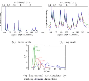
3.2 Log-normal distributions describing the domain diame-ters for various virtual powders considered here . . . 86
3.3 Selected atomistic domains from virtual powder 1. . . . 87
3.5 Selected atomistic domains from virtual powder 3. . . . 89
3.6 Selected atomistic domains from virtual powder 4. . . . 90
3.7 Selected atomistic domains from virtual powder 5. . . . 91
3.8 Selected atomistic domains from virtual powder 6. . . . 92
3.9 Selected atomistic domains from virtual powder 7. . . . 93
3.10 Intensity distributions from three domains of virtual powder 6 . . . 94
3.11 Fitted convergence behavior of ensemble-averaged diffracted intensity from virtual powders. . . 95
3.12 Ensemble-averaged powder diffraction data of sample 1. 97
3.13 Ensemble-averaged powder diffraction data of sample 2. 98
3.14 Ensemble-averaged powder diffraction data of sample 3. 99
3.15 Ensemble-averaged powder diffraction data of sample 4. 100
3.16 Ensemble-averaged powder diffraction data of sample 5. 101
3.17 Ensemble-averaged powder diffraction data of sample 6. 102
3.18 Ensemble-averaged powder diffraction data of sample 7. 103
3.19 Constrained fit of the powder diffraction data from sam-ple 3, and associated and Williamson-Hall analysis . . . 107
3.20 The powder diffraction data of sample 4, fit using a con-strained model, and the associated and Williamson-Hall plot . . . 111
3.21 Unconstrained fitting of the powder diffraction data from sample 4 . . . 114
3.22 Constrained fitting of the powder diffraction data from sample 6 . . . 117
3.23 Unconstrained fitting of the powder diffraction data from sample 6 . . . 119
3.24 Powder diffraction data of sample 7 fit using a con-strained approach, along with a Williamson-Hall plot. . 120
3.25 Fit of the diffraction data from sample 1 by directly computing the FT . . . 125
3.26 Powder diffraction data from sample 2 fit by directly computing the FT . . . 127
3.27 Fit of the powder diffraction data from sample 3 by di-rectly computing the FT . . . 128
3.29 Fit of the diffraction data from sample 5 by directly computing the FT . . . 130
3.30 Powder diffraction data from sample 6 fit by directly computing the FT . . . 132
3.31 Fitting diffraction data from sample 7 by directly com-puting the FT. . . 133
4.1 The unit cells of two sp3-bonded polytypes of boron nitride139
4.2 Common layer structure for the c-BN and w-BN polytypes144
4.3 Finite state machines representing the Markov process for the case of c-BN and w-BN polytypes, considering different interaction rangesR . . . 145
4.4 Powder diffraction data of the BN samples, with residual from both fitting approaches . . . 146
4.5 An atomistic BN domain highlighting bands showing local polytype symmetry . . . 149
4.6 Probability distributions describing the nanostructure of sample 1, derived from random sampling of refined stochastic process . . . 151
4.7 Atomic scale structure of the BN samples as extracted from powder diffraction data fitting. . . 154
4.8 Probability of finding a layer or band of a certain poly-type symmetry within each BN sample . . . 155
4.9 Nano and microstructure of the BN samples as extracted from powder diffraction data fitting. . . 156
Introduction
1.1
Historical perspective
A large portion of the field of materials science is focused on under-standing and exploiting underlying patterns in relative atomic posi-tions within solid materials. For reasonably ordered materials, such understanding and exploitation rests firmly on the pillars of
crystallog-raphyanddiffraction, which together provide the theory and practical
tools to measure and decode these patterns.
Phenomena characterized by diffraction, or the scattering and result-ing interference or superposition of waves, are pervasive within the natural world. In fact, the color blue as seen in vertebrates can be attributed solely to diffraction of visible light[1]. This suggests that Mother Nature has been exploiting diffraction phenomena long before
Homo Sapienseven contemplated the wave nature of light.
the new diffraction phenomena, and provided a simple mathematical relationship to compute inter-atomic spacings based on the position of what would soon be called “Bragg spots” [5]. With these pioneering experiments, von Laue and the Braggs launched the field of X-ray crys-tallography and earned themselves separate Nobel Prizes in physics.
Many of the theoretical underpinnings ofcrystallography, or the study of how objects or atoms fill space, were actually known before diffrac-tion facilitated the measurement of atomic posidiffrac-tions. In 1892, a com-plete list of the 230 three-dimensional space groups, based on argu-ments of group theory and including rigorous mathematical descrip-tions, was enumerated in personal communications between the math-ematicians Fedorov and Schönflies. This work laid the foundation for the future of diffraction based crystallography.
In the years since the inception of diffraction and crystallography, 29 Nobel Prizes have been awarded for work related to these topics. It is also evident that the field of materials science, fueled largely by crys-tallography and diffraction, has quite literally been the driving force behind many of the technological leaps and bounds of the last century, from Moore’s law to modern medicine. The importance of these topics is then clear, from both a practical and theoretical perspective.
1.2
Goals and motivations
The novel components of this work are focused largely on the close investigation of diffracted X-ray intensity distributions from nanopow-ders showing stacking disorder (or one-dimensional disorder). Addi-tionally, a general goal of this work is also to give a broader overview of what can be considered an emerging field of diffraction techniques in general: modeling of diffracted intensity distributions without empiri-cal assumptions on the constituent profile shapes, positions, or relative intensities.
resulting availability of pattern decomposition softwares have largely simplified and expedited these processes [6–8]. Such whole pattern fit-ting approaches are based on the hypothesis that diffracted intensity distributions can be modeled as a sum Bragg peaks, or line-profiles, with shapes, positions, and relative intensities constrained by simple models [9–11].
The recent interest in nanomaterials, however, gives justification for abandoning such a hypothesis. These materials often show novel and useful properties and are characterized by spatially anisotropic and inhomogeneous order on nanometer scales. This complex structure, along with instrumental optics, act as a convolution [12] on an instru-ment source profile to create a similarly complex diffracted intensity distribution frequently at odds with the previously mentioned simple models [13, 14]. The failure of traditional crystallography based as-sumptions in this case has been called “the nanostructure problem” [15]. It represents a significant roadblock for materials scientists and engineers [16], and its solution requires a new approach.
The first true steps away from traditional assumptions were made by Cheary and Coelho in thefundamental parameters (FP)approach [9]. This technique uses the physical parameters of the diffractometer, such as the divergent slit angle, the length of the X-ray anode, or the angular aperture of the Soller slits, directly within physical models to compute the instrumental effect on the measured intensity distribution. These models provide a complete and physical description of the instrumental line-profile shape, position-shift, and relative intensity across the full angular range of the diffractometer. A FP instrumental line-profile then shows all the anisotropy and asymmetry entailed by the specific diffractometer set-up without the need to invoke empirical profiles.
While the work of Cheary and Coelho as implemented in the TOPAS software package [8] has allowed crystallographers to physically model
theinstrumental effect on diffracted intensity distributions, simple
em-pirical models are still frequently used to represent thesample-related
choice ofwhichempirical profile to use is however quite arbitrary, and could bias the result of the analysis [19, 20]. Furthermore, the exact details of the sample nanostructure are hidden subtly in profile asym-metries, shifts, and other fine details, which are themselves masked by the effect of the instrument. Assuming an empirical profile shape to represent the sample signal can obscure these details completely. Using more complex models including asymmetric and shifted (but still em-pirical) profiles introduces further complications, as the relationship be-tween asymmetries/position shifts and structure/microstructure must be arduously derived explicitly for each material [21].
Surprisingly, the theoretical foundations for computing sample-related diffracted intensity distributions directly without empirical approxima-tions have existed for many years. In general each is based on express-ing how a physical phenomena perturbs the ideal crystal lattice or unit cell, and then propagating the perturbation to the Fourier transform (FT)of the crystal. In 1940 Ewald first suggested directly evaluating the FT of a crystal to obtain the diffracted intensity [22]. Shortly after, Stokes and Wilson presented a strategy (and several formulas) for directly computing the anisotropic line-profiles due to finite crystals with various morphologies and arbitrary atomic structure [23]. Wilkens later provided expressions for the anisotropic line-profile shapes asso-ciated with microstrain due to dislocations [24]. In his book originally published in 1969, Warren outlined an approach to computing the line-profile associated with planar defects in close packed structures [21]. A more general approach for one-dimensional disorder was outlined even earlier by Hendricks and Teller [25]. Probably owing to a lack of computational power, most of these approaches have been usedonlyto arrive at explicit expressions for thechangein profile position,FWHM, or asymmetry associated with these phenomena. These changes are extracted from powder diffraction data by pattern decomposition (em-pirical profile fitting) and then fed into the explicit expressions.
Recently in a series of papers, Scardi and Leoni outlined the collection and implementation of many of these approaches in what they have calledwhole powder pattern modelling (WPPM), where parameters of the sample, such as the shape of the CSDs and the associated CSD
functions [20,26,27]. This was followed quickly by a similar approach proposed by Ribárik et al.[28]. The two techniques have been imple-mented in the PM2K [29] and MWP-fit [28] software packages and have proven to be rather useful at extracting real microstructural informa-tion from materials [30–38], but are unfortunately not yet as pervasive as theFPapproach.
Within this work, Chapter2gives a review of some above-mentioned strategies to derive direct expressions for diffracted intensity distri-butions from nanocrystalline or one-dimensionally disordered samples. The general paths followed there can be used to derive intensity distri-bution equations considering other perturbations to ideal crystal struc-tures. This is in fact the route taken at the end of this chapter, where a new generalized model is presented for polydisperse nanocrystalline materials showing extensive stacking disorder.
In Chapter3the direct expressions presented in Chapter2are tested in several virtual diffraction experiments. The methods of virtual pow-der “synthesis” are outlined, along with the approach for carrying out a virtual diffraction experiment using the Debye scattering equation (DSE). The synthetic powder diffraction patterns from virtual powders with various nano and microstructures are compared and discussed. These powder patterns are then characterized following different ap-proaches from Chapter 2 to assess the validity and accuracy of those different models.
In Chapter 4, a number of different samples of industrially relevant
boron nitride are considered. Two different hypotheses regarding the nature of the nanostructure of these samples are tested, entailing the use of two different diffraction data fitting approaches from Chapter
Modeling diffraction
The diffracted intensity distribution from a collection of atoms can be computed directly by following two general routes. With what are typ-ically calleddirect-space (DS)approaches, all atomic positions within eachdomain are specified explicitly and used directly to build the in-tensity distribution without any assumptions regarding long-range or-der. While DS approaches allow for true atomic scale control over the intensity distribution, the required computational overhead scales quadratically with the number of scatterers (atoms) [39] and with the sixth power of the domain linear dimensions. This can lead to in-tractable computation times if the mean domain size is large and the atomic-configuration space of the sample is broad, as with broad crys-tal size distributions or complex stacking disorder. DSapproaches are explored in Chapter3.
The presence of three-dimensional translational periodicity such as that characterizing traditional crystals can be exploited to achieve sig-nificant mathematical simplifications and a reduction of computational overhead. This entails working in a Fourier transformed space, or
reciprocal-space (RS), where the elastic scattering of periodic objects can be represented more simply. Imperfections can be treated as per-turbations to the crystal lattice or unit cell, and their effect on the diffracted intensity distribution can be treated. Understanding such perturbations is the primary focus of this chapter.
polarization correction. Following this, in Section2.3a review of X-ray scattering from an isolated atom is given, leading to the typical atomic form factor description. Next, a mathematical description of a perfect, spatially infinite crystal, and its associated kinematic diffraction behav-ior is presented in Section 2.4. It is here that the traditional structure factor of the unit cell appears, as well Bragg’s law [5] for calculating line-profile positions. Following this, a review of the mathematical description of otherwise perfect, spatially finite crystal is given in Sec-tion2.5, along with the elastic scattering and interference that results from such objects. A general approach for representing an ensemble-averaged crystal showingdisorder in one direction is shown in Section
2.6, with expressions for computing the associated diffracted intensity distribution. This section offers some novel extensions to previous work in the field. In Section 2.7the general and physical models for crystal size, elaborated in Section 2.5, are used with the models for stacking disorder, outlined in Section 2.6, to give a novel and general RS de-scription of diffraction from polydispersed, nanocrystalline materials showing extensive linear disorder.
Any of the above described scattering models can be used to un-derstand real samples. By assuming a specific model with appro-priate initial parameters, a theoretical intensity distribution can be computed. An attempt can be made to minimize the total (weighted and/or squared) difference between the observed and calculated inten-sity distributions by refining the model parameters as constrained by the model assumptions. If a suitable solution is found, it can provide a best guess for the crystal structure (Rietveld analysis [11]) or the sample microstructure and defect content (line-profile analysis (LPA)
[12, 17–19]). If a suitable solution is not found, it can be necessary to start the process over, altering or abandoning some of the initial as-sumptions regarding crystal structure, unit cell symmetry, or empirical profile shape.
2.1
Practical examples: Nickel
case of metallic nickel. This choice was made based on the relative simplicity of the nickel structure, as complex abstract concepts can be demonstrated without introducing additional structural complications.
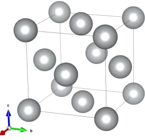
Figure 2.1: A perspective view of theface-centered cubic (fcc)unit cell for metallic nickel.
In the bulk form, metallic nickel adopts thefccstructure, with space group F m¯3m and a lattice parameter of 3.52 Å[40, 41]. A perspec-tive view of a bulk nickel unit cell is shown in Figure 2.1. Interest-ingly, nanocrystalline nickel is stable in both the fcc and hexagonal close packed (hcp) polytypes [42], strongly suggesting the possibility of both polytypes existing simultaneously interlayered within single nanocrystals.
Such polytype interlayering is an extreme case of stacking disorder which manifests in close-packed structures in a more dilute form as stacking faults, namely twin or deformation faults. Projections of the
written as
al=−
ac
2 + bc
2 (2.1a)
bl=−
bc
2 + cc
2 (2.1b)
cl=
1
3∥ac+bc+cc∥, (2.1c) whereac, bc, andcc are the typical cubic unit cell vectors. This layer
does not have a third lattice vector, as it shows only two-dimensional
periodicity. It is however a three-dimensional object with a layer thick-ness cl. The symmetry of this new layer unit cell is best described
with the sub-periodic layer groupp6/mmm(number 80) [43], with one nickel atom at Wyckoff position 1a. This layer unit cell is shown in Figure 2.2b.
(a)fccunit cells (b) common layer unit
cell (c)hcpunit cells
Figure 2.2: In (a), a projected view of severalfccnickel unit cells is shown, with the Warren layer type identified at left, and relative translation identi-fied at right. The same is shown in (c) for several idealizedhcpnickel unit cells. In (b), the layer unit cell common to both polytypes is shown, both in a top and front view. The indicated directions are with respect to the lattice of the closest pictured structure. Forward or backward relative translations are indicated by the color blue or red, respectively
are related by a “forward” shift, represented by the relative position vector Rf = a3l −b3l +clˆz, or the layers are related by a “backward”
shift, represented by the relative position vector Rb=−a3l+b3l +clˆz.
This description is consistent with the Hägg approach [44], where “for-ward” and “back“for-ward” are represented by “+” and “-,” and can be contrasted with the work of Warren, who described the two polytypes based on the three absolute positions of the atomic scale layers, de-scribing thefccpolytype as an. . . ABCABC . . .sequence and thehcp
polytype as an. . . ABAB . . .sequence [21]. These relative and absolute notations are also shown in Figure2.2.
2.2
A single scattering center
To begin, scattering from a single free electron is considered, as de-picted schematically in Figure 2.3. If a plane-wave of X-ray radiation with wavelengthλand wave-vectork0, where∥k0∥=k0= 1/λ,
inter-acts with a free electron, the electron oscillates due to the electric field
E0of the incident X-ray and radiates X-rays with electric field Ef. If
the spherical wave is observed at a distance rand scattering angle 2θ with respect tok0, then it appears as a plane-wave with wave-vectorkf
and electric field Ef/r. The momentum transfer vector or scattering
vector scan be defined as the difference between the final and initial
wave-vectors,s=kf−k0. If the interaction is purely elastic (Thomson
scattering) then k0 =kf, with ∥s∥ ≡ s = 2sinλ θ. In the elastic case,
the electric field of the scattered radiation can be written in terms of
E0and the Thomson scattering cross section,Ef = e
2
mec2rE0. Inelastic
(Compton) scattering is not considered in this work.
The degree and direction of linear polarization of the incident beam
Qcan be written in terms of components of the time averaged squared electric field, or intensity, that are parallel (∥) and perpendicular (⊥) to the plane of incidence
Q=⟨E0⊥⟩
2− ⟨E 0∥⟩2 ⟨E0∥⟩2+⟨E0⊥⟩2
=I0⊥−I0∥
I0⊥+I0∥
=I0⊥−I0∥
I0
. (2.2)
Figure 2.3: An X-ray with wave-vectork0and electric fieldE0impinging on a free electron with charge -eand massme. The radiation, with electric field
Ef, is elastically scattered tokf. The geometric meanings of the scattering vectorsand of the scattering angle2θare also shown.
By geometrical arguments (Figure2.3) the scattered intensity compo-nents can be written in terms of the incident intensity compocompo-nents as
If∥= e
4
me2c4r2I0∥cos
22θandI
f⊥= e
4
me2c4r2I0⊥. The total scattered
in-tensityIf can then be written as a sum of its components as a function
of the scattering vector or angle,
If(θ) =If⊥+If∥
= e
4
me2c4r2
I0⊥+
e4
me2c4r2
I0∥cos22θ
= e
4
me2c4r2 (
I0⊥+I0∥cos22θ )
= e
4
me2c4r2I0 (
(1 +Q) + (1−Q)cos22θ
2
)
. (2.3)
The last factor in equation 2.3 is typically called the polarization factorP F, and it indicates that the elastically scattered intensity isnot
dependent on the wavelength, but rather onboththe scattering angle 2θ
andthe degree and direction of linear polarization of the incident beam
P F is initially 1 at θ= 0, decreasing to a minimum of 1/2 whenθ= 45◦, and increasing again to 1 atθ= 90◦. When the incident radiation is polarized completely perpendicular to the plane of incidence, such as in most synchrotron X-ray sources, then Q= 1andP F = 1, showing no dependence on the scattering angle.
While these results are absolutely essential for correctly interpreting diffraction data, they generally lead to fluctuations in the diffracted intensity distribution which are dependent only on the experimental configuration. These dependencies include the initial beam intensity or polarization rather than the atomic, nano, or microstructure of the sample. It is however precisely this sample-specific information that is the focus of this work. For the sake of compactness then, the polariza-tion factor, initial beam intensity, and Thomson cross secpolariza-tion terms are omitted from the equations within the following sections, where the elastically diffracted intensity distributions from various different types of crystals are elaborated. In practice, only factors that vary with scattering angle, such as the polarization factor, need be consid-ered explicitly. The other constant terms involving the Thomson cross section can be effectively absorbed into a general scale factor.
2.3
An isolated atom
While an individual electron can often be handled as an isolated point charge, an atom is a collection of electrons best described in terms of a number density function U(r), wherer is a position vector relative to the origin, here taken as the center of the atom. The total number of electrons contained in a volume element dV at position r of such an atom is U(r)dV, while the total charge in this volume element is e U(r)dV. Figure2.4shows a hypothetical two-dimensional projection of a possible electron density function along with a scattering event.
If an X-ray with wave-vector k0 scatters elastically from the charge
element e U(r)dV to a new wave-vector kf, the scattering event is
Figure 2.4: A schematic depiction of an X-ray with wave-vector k0 im-pinging on an isolated atom. The X-ray scatters elastically from the charge elemente U(r)dV at positionrto the new wave-vectorkf.
difference can be approximated by considering only the spatial distance r between the two charge elements. Through geometric arguments, the phase difference is then −2πr·s. It is much more convenient to adopt the time-invariant complex phasor notation and write the phase difference as e−2πır·s. This allows the scattered wave amplitude as
observed at rP, resulting from the superposition of the two scattered
waves, to be written ase U(r)e−2πır·sdV. As mentioned at the end of
Section2.2, a factor including Thomson cross section and polarization effect has been suppressed for brevity.
The electron density function is extended in space, so the phase differ-ence from all volume elements must be considered by integration. In this way, the scattered wave amplitude as a function of the scattering vector is
φ(s)=
∫
U(r)e−2πır·sdV. (2.4)
typically called the atomic form factor f(s) ≡ φ(s). If the atom is spherically symmetric, then the atomic electron density depends only on the magnitude of the position vector,∥r∥=r, and the atomic form factor depends only on the magnitude of the scattering vector.
It should be mentioned that the treatment of the atom in this way assumes classical scattering. In reality, atoms are quantum objects with sharp absorption lines at well-defined energies, associated with intra-atomic electronic excitations. These absorption lines necessitate what is calledanomalous scatteringand dictate that the atomic form factor formally depends onboththe scattering vectorsand the energy of the incident X-rays ℏω. This phenomena can be handled by introducing a perturbation to the amplitude and phase of the atomic form factor. The new anomalous atomic form factor can be written as
f0(s,ℏω)=f0(s)+Δf′(ℏω)+ıΔf′′(ℏω), (2.5)
wheref0(s)represents the typical, spherically symmetric atomic form factor, while Δf′(ℏω)andıΔf′′(ℏω)indicate the effect of anomalous scattering on the magnitude and phase of the form factor, respectively. Energy dependent values for Δf′(ℏω) and ıΔf′′(ℏω) for various iso-lated atoms and ions can be found tabuiso-lated in the International
Ta-bles for Crystallography Volume C [45] or, perhaps more conveniently,
online [46].
Practically, the spherically symmetric atomic form factor is approxi-mated analytically in the scattering vector range 0<s < 225π Å−1 as a sum ofsdependent Gaussian functions following Cromer and Mann [47]. Using this approach, the atomic form factor can be can be written as
f(s)=
4 ∑
i=1 aie−bi
s2
4 +c. (2.6)
Equation2.6has been fit using spherically-averaged electron density maps computed with quantum theory for the most common isolated atoms and ions [48–50]. Tabulated values for ai, bi, and c are used
of electrons in a nickel atom (f(s= 0) = 28). The scattering factor then decreases monotonically with increasing scattering vector s or scattering angleθ.
0.00 0.5 1.0 1.5 2.0 2.5 3.0 3.5
5 10 15 20 25
s=2 sinHΘLΛHÞ-1L
f
H
s
L
Figure 2.5: The spherically symmetric atomic form factorf(s)of an isolated nickel atom, as approximated by equation2.6
2.4
Defect free, spatially infinite crystals
In this section, a mathematical description for kinematic diffraction from spatially infinite (unbounded) perfect crystals is outlined. It is clear that truly infinite objects do not exist practically, but in the context of this work, a crystal can be considered “spatially infinite” if it is much larger than the coherence length of the probe radiation. For typical laboratory diffractometers, this is about 100 nm, while for synchrotron X-ray sources, the coherence length varies by beam-line. While it may seem impractical a discussion of this type helps to introduce some general topics such asDSandRSlattices, Bragg’s law, the structure factor of the unit cell, and the so-called powder averaging of the diffracted intensity distribution. In general these concepts alone are sufficient in some cases to interpret diffraction data.
2.4.1 Electron density
crys-tal lattice. The Dirac delta distributionδ(r)facilitates this description, and it is useful to review some properties of these distributions:
∫ ∞
−∞
g(r)δ(r−T)dVr=g(T) (2.7a)
∫ ∞
−∞
aδ(r−T)dVr=a (2.7b)
g(r)∗δ(r−T)=
∫ ∞
−∞
g(τ)δ(r−T−τ)dVτ =g(r−T), (2.7c)
where∗represents the convolution operation,ais a scalar,Tis a real valued position vector, and dVrindicates that the integration is over
volume elements with respect to the spatial coordinater.
Ewald conveniently represented a lattice function as an infinite sum of these distributions, where each term represents one lattice point and is translated by a scaled lattice vector, ua+vb+wc[22], whereu,v, andware integers. The lattice function is written with this description as
z(r)≡
∞
∑
u=−∞
∞
∑
v=−∞
∞
∑
w=−∞
δ(r−ua−vb−wc)=∑
uvw
δ(r−ruvw),
(2.8) and represents a three-dimensionally periodic lattice that is described by one of the 14 possible three-dimensional Bravais lattices. The lattice function in equation2.8 evaluates to one of two values, either
z(r̸=ua+vb+wc)= 0
or
z(r=ua+vb+wc)=δ(0),
Further, each term in the lattice sum of equation2.8obeys the integra-tion properties outlined in equaintegra-tions 2.7a, 2.7b, and 2.7c, properties that will be exploited in the following.
potential; for X-ray scattering, this is electron density. The block used to dress the lattice is called the unit cell electron density, and contains
n atoms. It can be represented as a sum of the electron densities Up(r)of each isolated, spherically symmetric atomp, translated by the position vector of the atom rp =xpa+ypb+zpcwhere xp, yp,andzp
are fractional coordinates. Using this approach, the electron density of the unit cell can be written as
n
∑
p=1
Up(∥r−rp∥). (2.9)
The symmetry within the unit cell outlined in equation2.9is described by one of the 230 three-dimensional space groups. A spatially infinite crystal is then represented mathematically as the convolution of the unit cell and crystal lattice, written as
ρ(r)=
n
∑
p=1
Up(∥r−rp∥)∗z(r). (2.10)
The convolution in equation 2.10 exploits the convolution property of the Dirac distributions shown in equation2.7cto translate one unit cell to each lattice point, and creates a perfect, spatially infinite crystal. With this, the electron density can be written as
ρ(r)=∑
uvw n
∑
p=1
Up(∥r−rp−ruvw∥). (2.11)
In the next section the elastic scattering behavior of this object is investigated.
2.4.2 Scattering
The wave amplitude elastically scattered from the object represented in equation 2.11is found by the same process as outlined in Section
2.3. By integrating the product of the crystal electron density and the associated phasor term over all space, the scattered wave amplitude is written as theFTof equation2.11, or as
φ(s)=F
[ ∑
uvw n
∑
p=1
Up(∥r−rp−ruvw∥) ]
Recalling thatF[f(∥r−a∥)] =F[f(r)]e−2πıa·s, equation2.12can be written as
φ(s)=∑
uvw n
∑
p=1
F[Up(r)]e−2πırp·se−2πıruvw·s. (2.13)
However, F[Up(r)] is the scattered amplitude from an isolated atom or the atomic form factorfp(s)as presented in equation2.4in Section
2.3, while ∑n
p=1F[Up(r)]e−
2πırp·s represents theFT of the unit cell electron density in equation2.9. ThisFTis usually called the structure factor of the unit cellF(s), and is defined as
F(s)≡
n
∑
p=1
F[Up(r)]e−2πırp·s=
n
∑
p=1
fp(s)e−2πırp·s. (2.14) With this definition, the scattered wave amplitude in equation 2.12
can be rewritten as
φ(s)=F(s)∑
uvw
e−2πıruvw·s. (2.15) The diffracted intensity distribution is the squared modulus of this complex wave amplitude, and can be written as
I(s)=|φ(s)|2=
(
F(s)∑
uvw
e−2πıruvw·s
)(
F(s)∑
uvw
e−2πıruvw·s
)∗
=|F(s)|2 (
∑
uvw
e−2πıruvw·s
) ( ∑
u′v′w′
e2πıru′v′w′·s
)
=|F(s)|2 ∑
u′v′w′
∑
uvw
e−2πı(ruvw−ru′v′w′)·s, (2.16) where the superscript * indicates the complex conjugate, and the sums in each factor are explicitly over different sets unit cell translation in-dices, either uvw or u′v′w′. The double lattice summation of phase terms in equation2.16can be transformed into a newRSlattice func-tion following Guinier [51], defined as
Z(s)≡
∞
∑
h=−∞
∞
∑
k=−∞
∞
∑
l=−∞
δ(s−ha∗−kb∗−lc∗)=∑ hkl
δ(s−shkl),
where the triple sum is abbreviated ∑hkl, and ha∗+kb∗ +lc∗ is defined as shkl, or the scattering vector associated with the hkl RS
lattice point. By convention, the integers h,k, and l are called Miller indices, and each shkl point is often called a Bragg point. The RS lattice vectors, a∗, b∗, and c∗ are defined as cyclic cross products of theDSlattice vectors, normalized by the unit cell volume, and can be written explicitly as
a∗≡ b×c
(b×c)·a, b
∗≡ c×a
(c×a)·b, c
∗≡ a×b
(a×b)·c. (2.18)
With this, the intensity distribution in equation 2.16can be written as
I(s)=|F(s)|2∑
hkl
δ(s−shkl). (2.19)
Typically this equation is separated into the sum of intensity contribu-tion arising from each individual hkl Bragg point, and equation2.19
is written as
I(s)=∑ hkl
Ihkl(s) (2.20)
where
Ihkl(s) =|F(s)|
2
δ(s−shkl).
By equation2.20, the diffracted intensity distribution in RS due to a spatially unbounded perfect crystal can be visualized as an infinite, periodic RS lattice of Dirac distributions, where each distribution is weighted by the squared magnitude of the structure factor of the unit cell, evaluated at the lattice point shkl. The periodicity of the RS
lattice describing the intensity distribution is dependent upon theDS
lattice describing the crystal, while the total intensity weighting each lattice point is dependent upon the type and arrangement of atoms in the crystal unit cell.
2.4.3 Powder averaging
Equation 2.20 gives the diffracted intensity in three-dimensional RS
scientists are often more interested collections of many independently scattering crystals, such as a polycrystalline body or a powder. The following section will assume an ideal powder sample composed of the objects described in the previous section. In the context of this work an ideal powder is composed of many crystals showing a smooth uniform distribution of spatial orientations.
The diffracted intensity from such a powder represents the average
intensity over all possible crystal orientations. Rather than averaging the electron density of the crystal as expressed in equation 2.11, the orientation average is typically performed on the diffracted intensity distribution itself, as expressed in equation 2.20. The intensity dis-tribution obtained from a powder then retains no information on the direction of the scattering vectors, and depends only on its magnitude s.
The averaging is done by evaluating the surface integral of equation
2.20over a sphere with constant radiuss. This is easiest in spherical co-ordinates, where the differential surface element is dS=s2sinθdθ dϕ.
The integration surface is typically called the powder diffraction sphere. The maximum radius of the sphere is determined by the wavelength of radiation used, and gives the portion of reciprocal space that can be explored with a given diffraction experiment. It is found by setting the scattering angle to180◦,smax= 2/λ. Within the powder integration,
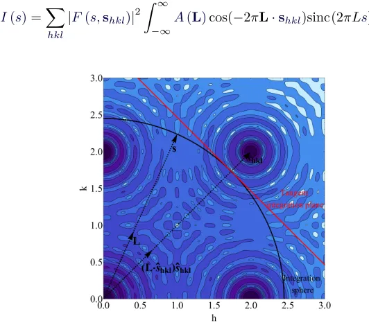
a weighting factor of1/4πs2is used to account for the decreasing like-lihood of a diffraction event occurring as sincreases. This weighting term is often called the Lorentz factor, but it is not usually maintained in this form following integration. The powder intensity is then written as
I(s)= 1 4πs2
∫∫
S
I(s)dS
= 1 4πs2
∫ 2π
0 ∫ π
0
I(s)s2sinθdθdϕ
= 1 4π
∑
hkl
∫ 2π
0 ∫ π
0
δ(s−shkl)|F(s)|2sinθdθdϕ (2.21)
The Dirac distribution δ(s−shkl), can be rewritten in spherical co-ordinates as 1
integration onθandϕis analytic, and equation2.21can be rewritten as
I(s)= 1 4π
∑
hkl
∫ 2π
0 ∫ π
0
δ(s−shkl)|F(s)|
2
sinθdθdϕ
= 1 4π
∑
hkl
∫ 2π
0 ∫ π
0
|F(s)|2
s2sinθδ(s−shkl)δ(θ−θhkl)δ(ϕ−ϕhkl)sinθdθdϕ
= 1 4πs2
∑
hkl
δ(s−shkl)|F(shkl)|
2
(2.22)
This gives the result that the diffracted intensity of an ideal powder of perfect, spatially infinite crystals is a sum of Dirac delta distributions with positions given by the RSlattice. The diffracted intensity is
in-finite whens=shkl, while it is exactly zero at all other points, when
s̸=shkl, that is
I(s)=
{
δ(0)|F(shkl)|2
4πs2 , ifs=ha∗+kb∗+lc∗=shkl 0, ifs̸=shkl
. (2.23)
This is not particularly useful, but is a direct result of considering a powder of perfect infinite crystals completely bathed in X-rays.
Speaking more empirically, it is known that instrumental aberrations and deviations from perfect crystallinity both act as convolutions to smear the diffracted intensity [12], leading to measured powder diffrac-tion data that never contains Dirac delta distribudiffrac-tions. If an empirical profile functionP(s)is adopted to approximate this effect, the smeared powder intensity distribution can be written as
Iempirical(s)=P(s)∗I(s)= ∑
hkl
|F(shkl)|
2
4πs2
hkl
P(s−shkl). (2.24)
Physically this implies that the total observable intensity of a Bragg point is finite and proportional to the squared magnitude of the struc-ture factor evaluated at the Bragg point.
speaking this form of the Lorentz factor is only accurate under the assumptions of an ideal powder of perfect, spatially infinite crystals. Defects and spatial boundedness entail a different form of equation2.20
and a different approach to powder integration, leading to a different Lorentz factor. This is reviewed in Sections 2.5and2.6.
Each delta distribution in equation 2.22 or each profile function in equation 2.24 is located at the scattering vector shkl. Recalling the definition of the scattering vector from Section 2.2, this location can be converted to the more observable scattering angle through the re-lationship shkl = 2sinλθhkl. Recognizing that the nature of the FT operation dictates that the hkl Bragg point corresponds to the dis-tances between (hkl) set of crystal planes implies thatshkl = 1/dhkl; wheredhkl is the spacing between the (hkl) set of crystal planes. This in turn leads to Bragg’s law λ = 2dhklsinθhkl, relating inter-atomic distances to measurable quantities in the observed powder diffraction pattern [5].
Two example powder intensity distributions, simulated assuming metal-lic nickel as outlined in Section2.1, are shown in Figure2.6. Both were computed by assuming unpolarized incident radiation, requiring a po-larization factor given by equation 2.3 with Q = 0. A wavelength of 1.54059Å was assumed, as it is a common condition in laboratory diffraction instruments where characteristic copper radiation is often used. In Figure 2.6a, equation2.22 was used, and each Delta distri-butions representing a Bragg peak is shown with an artificial width of 0.5◦ 2θand a height proportional to the relative intensity of the Bragg peak. In Figure 2.6b, the unrealistic intensity distribution presented in Figure2.6ahas been empirically broadened as per equation2.24by a Cauchy distribution with unit area and FWHMof 1◦ 2θ. The sym-metry of the nickelDS lattice dictates that a number of Bragg peaks (e.g. the {111} family) are degenerate in both powder position shkl and integrated intensity. The symmetry of the nickel unit cell entails that some Bragg peaks (e.g. the {110} family) lead to a structure fac-tor that is exactly zero, causing systematic absences in the intensity distributions shown in Figure 2.6.
(a) Dirac profiles (b) Cauchy profiles
Figure 2.6: The diffracted intensity distributions due to an ideal powder of perfect, spatially infinite nickel crystals is shown, assuming unpolarized cop-perKα1 radiation, leading to a polarization factor 1+cos2 2θ, as per equation 2.3. Bragg peaks are either shown as Dirac distribution with an artificial width of0.5◦ 2θ, as per equation 2.22, or as Cauchy distributions with a FWHMof1◦2θ, as per equation2.24.
of this kind has been hugely and undeniably successful at furthering material science, it was highlighted in Section 1.2 that the intrinsic assumptions on which it is based can be limiting when characterizing nanomaterials [16]. It is with these limiting assumptions in mind that the next section is presented, focusing on a physical representation of line-profile shapes due to the finite spatial extent of crystals.
2.5
Defect free, spatially finite crystals
(intensities add). Gelisio and Scardi studied the effect upon diffracted intensity of positional and rotational correlation between adjacent do-mains, finding that for domains larger than just a few nanometers
domain-domain interference effects were negligible with only a slight degree of misorientation betweendomains, possibly only detectable by advanced synchrotron light sources [52].
Many authors have sought to describe the diffraction effect of the fi-nite spatial extent of aCSD. Scherrer developed the so-called Scherrer formula. In 1918 he suggested that the FWHMof the diffraction line profile, in units of the scattering vector, is inversely proportionate to the thickness of the crystal [17]. This was extended in 1942 by Stokes and Wilson, who derived a strategy (and several formulas) for directly computing the anisotropic line-profiles due to finite crystals with var-ious morphologies and arbitrary atomic structure [23]. This has only recently been employed to directly compute line-profile shapes [20,26– 28]. The following section reviews some of these strategies and offers some novel extensions.
2.5.1 Electron density
To model spatially finite crystals, it is convenient to directly modify the spatially infinite electron density represented in equation 2.10. In 1940, Ewald proposed the use of a shape function for this modification [22], piecewise defined as either 1 inside or 0 outside the shape volume
Vc, written as
σ(r)=
{
1, ifr∈Vc
0, ifr∈/ Vc
. (2.25)
Applying σ(r) to the electron density function must be done with forethought, as the mathematical route employed has a direct impact on the surface termination of the domain, as pointed out by Ino and Minami [13]. If the shape function is applied after the lattice has been tiled with electron density, as proposed by Patterson and Ewald, the electron density is written [22,53]
ρ(r)=
(∑n
p=1
Up(∥r−rp∥)∗z(r) )
Figure 2.7: When the shape function acts on the infinite crystal electron density as in equation2.26the resulting spatially finite crystal has a “hard” boundary.
and the resulting density function represents the spatially infinite elec-tron density cut abruptly at the shape function boundaries, as seen in Figure 2.7. Using this description, some atoms with local origins com-pletely outside the domain volume Vc contribute electron density to
the finite crystal, while the electron density of surface atoms with local origins inside Vc is suddenly cut off. Although it may seem
unphysi-cal, this description is sufficiently accurate for largedomainsto a first approximation, where the fraction of surface atoms is small [13,54].
An alternative approach was proposed by Hosemann and Bagchi. First the shape function is applied to the lattice, which is then dressed or tiled with the unit cell electron density. With such an approach the
domain electron density is written as [55]
ρ(r)=
n
∑
p=1
Up(∥r−rp∥)∗ (
z(r)σ(r) )
. (2.27)
Figure 2.8: When the shape function acts on the infinite crystal electron density as in equation2.27the resulting spatially finite crystal includes only electron density from the atoms within unit cells associated with a lattice point within the crystal volume.
atoms in each unit cell associated with a lattice point withinVc, as seen
in Figure2.8. Adomaindescribed in this way also shows some strange features. Some atoms with local origins outside Vc are included fully
in the domain, while some atoms with local origins fully insideVc are
not included, as the unit cell they belong to was removed by the shape function.
Ino and Minami suggested that the atom be considered the most fundamental building block of a finite crystal, thus they proposed a
domainelectron density function where the shape function removes all electron density from all atoms with a local origin outsideVc, but that
retains the complete electron density of all atom with local origins in-sideVc, even if the diffuse electron density extends beyond the borders
of Vc [13]. An example is presented in Figure 2.9. Mathematically,
this requires translating the lattice function, rather than the atoms, by the fractional coordinaterpof thepthatom in the unit cell. The
Figure 2.9: When the shape function acts on the infinite crystal electron density as in equation 2.28 the resulting spatially finite crystal retains all electron density from all atoms with local origin inside the crystal volume.
density of thepthatom Up(r). A sum is then taken over all atoms in the unit cell. Following this route, the electron density is written [13]
ρ(r)=
n
∑
p=1
Up(r)∗
(
z(r−rp)σ(r)
)
. (2.28)
This approach is the most intuitive and physically realistic for de-scribing the shape of domainsin nanomaterials, as it most accurately reproduces the “intended” shape of thedomain as represented by the shape function. It does not introduce any unphysical features at the surface of the domain, such as those seen in Figure 2.7 or Figure 2.8. Thus equation2.28 is the preferred form of the domain electron den-sity for the following derivation of the intenden-sity distribution. It should be pointed out that the mathematical definition of the finite crystal
2.5.2 Scattering
Again, the scattered wave amplitude is represented by theFTof the electron density. Equation 2.28 can be transformed and the RS lat-tice in equation2.17can be substituted. Following this approach the scattered wave amplitude can be written as
φ(s)=F
[ n ∑
p=1
Up(r)∗ (
z(r−rp)σ(r)
)]
=
n
∑
p=1
F[Up(r)]
(
F[z(r−rp)]∗ F[σ(r)]
)
=
n
∑
p=1
fp(s)
((
Z(s)e−2πırp·s)∗ F[σ(r)]
)
. (2.29)
By making the definition S(s)≡F[σ(r)]equation2.29can be rewrit-ten as
φ(s)=
n
∑
p=1
fp(s) ((
Z(s)e−2πırp·s
) ∗S(s)
)
=
n
∑
p=1
fp(s)
( ∑
hkl
e−2πırp·shklS(s−s
hkl) ) =∑ hkl n ∑ p=1
fp(s)e−2πırp·shklS(s−s
hkl). (2.30)
The sum∑n
p=1fp(s)e−
2πırp·shklin equation2.30is similar to structure
factor outlined in Section2.4.2and written in equation2.14, but here it depends onboth the scattering vector magnitudesand the location of the Bragg pointshkl. This summation is here called the IM structure factor and identified as F(s,shkl), after Ino and Minami [13]. The dual dependence is a result of the new definition of the electron density function (equation2.28). By substitutingF(s,shkl)into equation2.30 the scattered wave amplitude can be written as
φ(s)=∑ hkl
The scattered wave amplitude is a sum inRS of theFTof the shape function translated to each Bragg point and weighted by the IM struc-ture factor. The squared magnitude of equation 2.31 represents the diffracted intensity distribution, and can be written as
I(s)=|φ(s)|2=
( ∑
hkl
F(s,shkl)S(s−shkl)
) ( ∑
h′k′l′
F(s,sh′k′l′)S(s−sh′k′l′)
)∗
.
(2.32)
Where each sum is explicitly over different sets of Miller incices, either hklorh′k′l′. The product can be grouped into the sum of two different products: those where hkl = h′k′l′ and those where hkl ̸= h′k′l′, allowing equation2.32to be re-written as
I(s)=∑ hkl
|F(s,shkl)S(s−shkl)|
2
+
∑ ∑
hkl̸=h′k′l′
F(s,shkl)F(s,sh′k′l′)∗S(s−shkl)S(s−sh′k′l′)∗. (2.33)
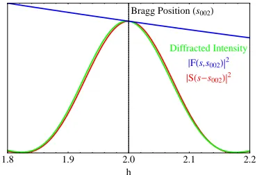
The second group of terms in equation 2.33wherehkl ̸=h′k′l′ is not necessarily zero. Since S(s) generally has spatial extent (it is not a Delta distribution), S(s−shkl) andS(s−sh′k′l′)∗ could overlap if thehklandh′k′l′Bragg points are close inRS. It would be convenient however to ignore the second group of terms in equation 2.33, as it is much too computationally expensive in its full form.
The approach shown so far in this section intrinsically assumes that the shape function and lattice function have coincident origins. A spe-cial case of equation2.33exists, where thedomainunder investigation is considered as an “average,” constructed by considering a uniform dis-tribution of all relative shape function origins. That is, equation2.33
(a) no shift (b) random shift
Figure 2.10: Schematic projections of the electron density from twodomains cut with the same shape function with different relative shape function trans-lations.
In general thedomain electron density as expressed in equation2.28
is not invariant under a translation of the shape function by t. Two
crystals formed by applying otherwise identical shape functions can show different surface termination, and even a different number of scattering centers or atoms, due to a different choice of shape function origin. Physically the averaging over all shits acts to “blur” the sur-face of thedomain, dictating that the realdomainunder consideration consists of an average of all possible surface terminations. This point is highlighted in Figure 2.15, which shows two distinct finite crystals, cut from the same infinite crystal by the same shape function with different relative displacements.
As an additional point, with increasing domain size, S(s) becomes more spatially compact, and as a result the cross terms in equation
2.33become increasingly negligible. This was explicitly highlighted by Guinier [51], but it is a generalization of the Scherrer formula [17].
I(s)=∑ hkl
|F