Volume 3 • Issue 4 • October 2017
ISSN 2206-4451
www.ajbssit.net.au
Nano Transistors Performance Analysis
Md. Shafiq Uddin
Department of EEE, Uttara University, Dhaka, Bangladesh
1. Introduction
Nanowires (NWs) are attracting much interest from those seeking to apply nanotechnology and especially those investigating nanoscience. Although conventional planar metal oxide semiconductor field effect transistor (MOSFETs) are approaching nanometer scale, their performance becomes limited by short channel effects, increasing OFF-state current, and poor electrostatic control of the channel (Taur and Ning, 1998). Unlike other low-dimensional systems, NWs have two quantum-confined directions but one unquantum-confined direction available for an electrical conduction. This allows NWs to be used in applications where electrical conduction, rather than tunneling transport is required. Due to their unique density of electronic states in the limit of small diameters, NWs are expected to exhibit significantly different optical, electrical, and magnetic properties to their bulk 3D crystalline counterparts.
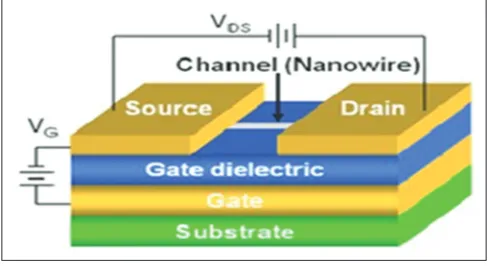
NWs are nanoscale structures which are frequently single crystal materials and are typically cylindrical in shape. They can be formed in a variety of materials including metallic (Ni, Pt., Au), semiconducting (silicon [Si], germanium [Ge], gallium arsenide [GaAs], indium arsenide [InAs], InP, GaN, etc.), and insulating (SiO2, TiO2) but are most frequently fabricated using semiconducting materials. They have fascinated attention not only because of their extremely small size but also their size causes new physics (quantum effects) to apply. This does not occur classically which can cause changes in material properties (Kamins, 2005). Three phenomena that are the most notable are (i) the diameter of NW decreases, the energy band gap can change; (ii) the diameter of NW can change the material’s character; (iii) ballistic transport without scattering can occur which can lead to notably improved device performance (Dreseelhaus et al., 2003). The reason which leads the researchers think about replacement of planar MOSFET is NW transistor (NWT) that has the strongest gate control over planar MOSFET and other proposed structures. Figure 1 shows a schematic structure of a NWT showing metal source and drain electrodes with the NW.
Abstract
Nanowire transistors (NWT) have attractive attention due to the feasible high performance and excellent controllability of device current. In this paper, the performance analysis of NWT made of different materials such as silicon, germanium, gallium arsenide, and indium arsenide are investigated. Self-consistent 3D simulations are used due to their 3D distribution of electron density and electrostatic potential. The output characteristics of the NWT are studied in details for all the materials of different transport orientations. NW, a 3D Poisson self-consistent simulator is used for simulation which can study the 3D transport in NWT considering phonon scattering based on the effective mass approximation.
2. Homogeneous NW-Based Devices
In the case of NWs with homogeneous structure and composition, Si NWs have most extensively been studied (Cui et al., 2003). This is due partly to the dominance of Si in the semiconductor industry, but also reflects the high-level of control of structure and doping demonstrated in fundamental Si NW growth studies (Zheng et al., 2004). In addition, other NW materials such as Ge, GaAs, InAs, GaN, and metal oxides have also received broad attention (Wang et al., 2003).
2.1. Si NWs
Researches on NWs began to accelerate in 1998, when Si NWs with diameters <20 nm and lengths >1 µm were demonstrated using a laser-ablation method (Morales and Lieber, 1998). The ability to prepare NWs with diameters <20 nm made it possible for the first time to produce devices that could approach a 1D limit desirable for high-performance transistors. Initial efforts led to demonstration of NWTs and basic devices configured using crossed NW geometry, including p-n diodes and bipolar transistors (Huang et al., 2001). However, the electrical properties of NWs in these initial studies were far from optimal, for example, leading to low apparent carrier mobility and large sample to sample variations.
2.2. Ge NWs
Ge NW devices have also been studied by several groups due to the higher electron and hole mobility compared with Si. Compared to Si NW, Ge NW devices are expected to have smaller contact effects because the smaller Ge band gap will yield a lower Schottky barrier at the metal/NW interface. For example, studies of p-type Ge NW devices with Pd S/D contacts yielded a hole mobility of 600 cm2/V.s
(Dayeh et al., 2007). In addition, complementary n-type and p-type Ge NW devices were demonstrated based on a surface doping approach to prevent uncontrolled sidewall deposition during the NW growth (Greytak et al., 2004). Prototype gate-all-around devices were also demonstrated by Zhang using atomic layer deposition and magnetron sputtering to uniformly coat an Al2 O3 dielectric layer and an Al gate layer. Compared with the back-gated Ge NW devices, the gate-all-around devices showed excellent subthreshold performance due to the improved electrostatics.
2.3. GaAs NWs
Now researchers have made high-performance transistors from a promising candidate material: GaAs NW. GaAs materials have higher charge mobility than Si switch ON and OFF faster than Si-based devices but the challenge is cost. GaAs wafers are much more expensive and far smaller than Si wafers. NWs offer a way around the wafer problem, because they should use less material. The growth of the wires is catalyzed by spots of gold, patterned in a tight line by electron-beam lithography onto a surface. As the chamber fills with gaseous precursors, the gold spots catalyze the deposition of solid GaAs. By controlling the ratio of
gallium and arsenide, and conditions such as temperature and pressure, it is shown that the gold catalyst moves along the surface as the NW grows, rather than leaving the surface and forming the NWs vertically. The NW arrays to make a type of high-performance transistor similar to those found in radar equipment and cell-phones. Each 10-µm-wide transistor contains about 30 NWs, along with three electrodes. A top electrode called a gate applies a voltage across the device to switch the NWs between conducting, or “ON” and insulating, or “OFF” states. In the ON state, charges flow between source and drain electrodes. The transistors have blistering switching speeds, turning ON and OFF 75 billion times a second, or at 75 GHz. The previous record for planar NWT s was 1.8 GHz. Researchers are also thinking that mobility of InAS is three times higher than GaAs, so if it is possible to make and if it works; then, we will get THz speeds.
2.4. InAs NWs
InAs NWs have widely been studied as a building block for n-type FETs. InAs is an attractive material for numerous reasons. First, its small effective electron mass (0.023 m) results in high-electron-mobility in bulk materials. Second, an electron gas layer is known to form at the surface of planar InAs due to Fermi level pinning in the conduction band. Third, the formation of an electron gas combined with the small band gap of 0.35 eV should relatively yield transparent contacts to InAs NW devices. Studies of InAs NWTs have yielded depletion-mode n-channel FETs with electron mobility on the order 3000 cm2/V.s (Dayeh
et al., 2007). The epitaxial growth of InAs NWs has led to the demonstration of vertical NW structures with a wrap-around gate with a low saturation voltage of 0.15 V (Bryllert et al., 2006).
3. Methodology
To deeply understand device physics of NWTs and to assess their ultimate performance limits, simulation work is necessary and important. In contrast to a planar MOSFET that has a uniform charge and potential profile in the transverse direction (NORMAL to both the gate and the source-to-drain direction). NWT has a 3D distribution of electron density and electrostatic potential. As a result, a 3D simulator is required for the simulation of NWTs.
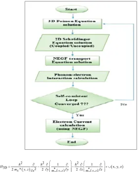
In this paper, a 3D self-consistent quantum simulation of NWTs based on the effective-mass approximation (whose validity in a scale device simulation has been established in Reference (Wang et al., 2004) is proposed. The methodology of this work is shown as flowchart in Figure 2. The calculation involves solution of a self-consistent 3D Poisson equation for the electrostatic potential. After that, the calculation involves solution of 2D Schrödinger equation with open boundary conditions for each cross section of the NWT to obtain the electron subbands (along the NW) and Eigen functions. The 2D Schrödinger by a mode space approach (coupled/uncoupled) is solved which provides both computational efficiency and high accuracy as compared with directorial space calculations. Coupled/uncoupled nonequilibrium green function (NEGF) transport equations are solved for the electron charge density. Phonon-electron interaction calculation is done with the self-consistent born approximation. The first step is repeated to calculate the electrostatic potential. If the self-consistent loop has converged, the electron current is calculated using the NEGF approach. Different transport models are implemented into simulator. In this paper, both ballistic NEGF model and dissipative NEGF models are discussed. Ballistic NEGF model gives the upper performance limit of Si, Ge, GaAs and InAs NWTs, and a dissipative NEGF model with a simple treatment of scattering with the Buttiker probes offers an efficient way to capture scattering in the quantum mechanical framework.
3.1. Coupled mode space (CMS) approach
In this part of the work, the CMS approach is briefly discussed and listed out the basic equations for the particular case of interest. In the 3D domain, the full stationary Schrödinger equation is given by:
H3Dψ (x,y,z) = Eψ (x,y,z) (1)
( ) ( ) ( ) ( )
2 2 1 2 1
x, y, z
3D 2 , 2 2 2
, ,
h h h
H * *
m * y zx x y m y z m y z y y z z z
∂ ∂ ∂ ∂ ∂
= − − +∪
∂ ∂ ∂ ∂
∂
(2)
Here, mx*, my* and mz* are the electron effective mass in the x, y and z directions, respectively; U (x, y, z) is the electron conduction band-edge profile in the active device. After the device Hamiltonian H is obtained, the electron density and current can be calculated using the NEGF approach. The NEGF Approach is a commonly used method for the simulation of nanoscale electronic devices. The retarded Green’s function of the active device is defined as:
G (E) =[E−H−∑s(E)−∑1(E)−∑z(E)]−1 (3)
Here, ∑S is the self-energy that accounts for the scattering inside the device (zero in the case of ballistic approach), and ∑1 (∑2) is the self-energy caused by coupling between device and the source
(drain) (Wang et al., 2004).
3.2. UnCMS approach
The unCMS approach gives quantum confinement and transport separately. In the simulation of NWTs, it is assumed that the shape of the Si body is uniform along the x direction. As a result, the confinement potential profile (in y z plane) varies very slowly along the channel direction. For instance, the conduction band-edge U(x, y, z) takes the same shapes but different values at different x. For this
reason, the Eigen functions ξ m(y, z, x) are 10 approximately the same along the channel. Hence, it is
assumed,
ξm (y,z;x) = ξm (y,z) (4)
The retarded Green’s function for mode m of the active device is rewritten as Wang et al., 2004.
Gm(E) = [ESm−hmm−∑m(E)−∑m(E)−s1 ∑m(E)]−1 (5)
3.3. NEGF formalism
The simulation of electronic devices generally contains self-consistent solution of the electrostatic potential and carrier distribution inside the device. Over the years, device engineers have improved our collective knowledge of carrier transport and semiconductor physics. Earlier treatment of electrons and holes as semi-classical particles with an effective mass was good enough to predict semiconductor device behavior and the drift-diffusion equation was adequate to describe carrier transport. MOSFETs have shrunk to Nanoscale dimensions, which have required a re-examination of this approach to device modeling. A more sophisticated analysis of the device physics is needed, such as the Nonequilibrium Green’s Function (NEGF) approach, to model devices all the way to ballistic level (<10 nm) (Anantram et al., 2008).
4. Simulation Results and Discussion
In this work, 3D “NW” simulator is used for the simulation of NWTs. The simulation software used for the modeling of NWT s is based on the work done by Hong-Hyun Park et al. and his colleagues at Purdue University (Park and Klimeck, 2010).
4.1. Simulation results
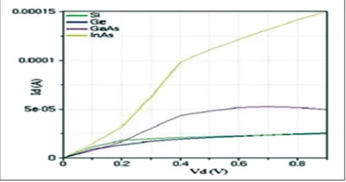
Because of longer simulation time, the unCMS NEGF transport is considered only. Although Si is the most common and economical material used in semiconductor industry, it has some limitations and maybe reaches its physical end soon. There are some other materials which are very active in research and exhibit some promising improvement over Si. Hence, the Si with other semiconductors for the NWT channel material is compared. The gate work function of 4.15 eV is used, which is for the metal Aluminum (Al). The NW diameter is considered to be 4 nm, oxide thickness of SiO2 is 1 nm, gate length is of 8 nm, and the source-drain extension length is of 8 nm each. The doping profile of 2×10²⁰/cm3 is considered for the source-drain extensions. The channel region doping is set to zero
which provides results similar to that of an intrinsic channel. The gate voltage is kept fixed at 400 mV and the drain current is extracted for different drain bias using Si as the channel material with unCMS approach. The same thing is repeated using Ge, GaAs and InAs as the channel material.
4.2. Discussion
It is inferred from the above Figures 3-5 that the NWT Ge, GaAs, and InAs as channel material has more ON current when compared with that of the Si counterpart for various crystal orientations (100, 110 and 111) with uncoupled mode transport. From the analysis of the different material’s NWTs, the orientation of 110 has less ON current compared with orientation of (100 and 111) for Si material. Ge, GaAs, and InAs have almost same ON current in all the crystal orientations.
5. Conclusion
Hence, conclusion can be drawn that Ge, GaAs, and InAs have NWTs have higher mobility than Si NWTs and InAs has the highest mobility.
Figure 3: Drain current (Id) vs. drain voltage (Vd) plot of nanowire transistor for four different materials (Si, Ge, GaAs, and InAs) with uncoupled mode space approach for 100 crystal orientations
Figure 4: Drain current (Id) vs. drain voltage (Vd) plot of nanowire transistor for four different materials (Si, Ge, GaAs, and InAs) with Uncoupled mode space approach for 110 crystal orientations
References
Anantram, M.P., Lundstrom, M., Nikonov, D. (2008), Modeling of nanoscale devices. Proceedings of the IEEE, 96, 1511-1550.
Bryllert, T., Wernersson, L.E., Froberg, L.E., Samuelson, L. (2006), Vertical high-mobility wrap-gated InAs nanow-ire transistor. IEEE Electron Device Letters, 27(5), 323-325.
Cui, Y., Zhong, Z.H., Wang, D.L., Wang, W.U., Lieber, C.M. (2003), High performance silicon nanowire field effect transistors. Nano Letters, 3(2), 149-152.
Dayeh, S.A., Aplin, D.P.R., Zhou, X.T., Yu, P.K.L., Yu, E.T., Wang, D.L. (2007), High electron mobility InAs nanowire field-effect transistors. Small, 3(2), 326-332.
Dreseelhaus, M.S., Lin, Y.M., Rabin, O., Jorio, A., Souza Filho, A.G., Pimenta, M.A., Saito, R., Samaonidze, G.G., Dresselhaus, G. (2003), Nanowires and nanotubes. Materials Science and Engineering C Biomimetic and Supramolecular Systems, 23(1-2), 129-140.
Greytak, A.B., Lauhon, L.J., Gudiksen, M.S., Lieber, C.M. (2004), Growth and transport properties of complemen-tary germanium nanowire field effect transistors. Applied Physics Letters, 84(21), 4176-4178.
Huang, Y., Duan, X.F., Cui, Y., Lauhon, L.J., Kim, K.H., Lieber, C.M. (2001), Logic gates and computation from assembled nanowire building blocks. Science, 294(5545), 1313-1317.
Kamins, T. (2005), Beyond CMOS eleactronics: Self assembled nanostructures. Journal of Electrochemical Society (ECS) Interface, 46-49.
Morales, A.M., Lieber, C.M. (1998), A laser ablation method for the synthesis of crystalline semiconductor nanow-ires. Science, 279(5348), 208-211.
Park, H.H., Klimeck, G. (2010), Quantum approach to electronic noise calculations in the presence of electron-phonon interactions. Physical Review B, 82(4), 125328.
Taur, Y., Ning, T.H. (1998), Fundamentals of Modern VLSI Devices. New York: Cambridge Press. p268.
Wang, D.W., Wang, Q., Javey, A., Tu, R., Dai, H.J., Kim, H., McIntyre, P.C., Krishnamohan, T., Saraswat, K.C. (2003), Germanium nanowire field-effect transistors with SiO2 and high-κ HfO2 gate dielectrics. Applied Physics Letters, 83(12), 2432-2434.
Wang, J., Polizzi, E., Lundstrom, M. (2004), A three-dimensional quantum simulation of silicon nanowire transistors with the effective-mass approximation. Journal of Applied Physics, 96(4), 2192-2203.
Zhang, L., Tu, R., Dai, H. (2006), Parallel core-shell metal–dielectric–semiconductor germanium nanowires for high-current surround-gate field-effect transistors. Nano Letters, 6(12), 2785-2789.