INTRODUCTION
The PbSe is important material for infrared detection. It is II – IV semiconductor having narrow band gap, which is used for photographic plates, selective photovoltaic absorbers and lasers1-6. Survey of literature shows that different techniques of deposition have been developed to obtain device grade PbSe thin films, among which chemical deposition, electro chemical deposition7-15. In the present work, systematic investigation of the effect of the preparation conditions on the optical properties and structural characterizations have been carried out. An interpretation of the determined optical constant variations in correlation with the corresponding structural and morphological parameters are presented.
EXPERIMENTAL Deposition of PbSe films
Polycrystalline PbSe films have been
Materials Science Research India Volume 3(2a), 271-278 (2006)
Optical properties of thermally evapourated
Lead Selenide thin films
S.R. JADHAV
1, P.H. PAWAR*, U.P. KHAIRNAR
2and G.P. BHAVSAR
21Department of Physics, Rashtriya College, Chalisgaon - 424 101 (India) *Department of Electronics, Jai Hind College, Dhule - 424 002 (India)
2P.G. Department of Physics, Pratap College, Amalner (India)
(Received: September 21, 2006; Accepted: November 17, 2006) ABSTRACT
Polycrystalline Lead Selenide Thin Films have been deposited onto glass substrate at 300K by thermal evaporation. The XRD study shows that all samples were polycrystalline having FCC structure. The surface morphology shows that as grown films are polycrystalline with crystallites randomly scattered on the surface. The transmittance and reflectance have been measured at normal and near normal incidence respectively, in the spectral range 200 to 2600 nm. The dependence of absorption coefficient a on the photon energy have been determined. Analysis of the result showed that for lead selenide films of different thicknesses, direct transition occurs, with band gap energy in the range 0.8 ev to 1.36 ev. Refractive indices and extinction coefficient have been evaluated in the above spectral range.
Key words: Optical properties, Lead selenide thin films.
deposited via sublimation of compound in a vacuum higher than 10-5 Torr under controlled growth condition of various thicknesses. Lead Selenide material used was in powder form. This was of “Aldrich Chemical Co.” makes having purity of 99.999%. The substrates used were glass slides of dimensions 75 x 25 x 1 mm. The glass slides were cleaned with warm dilute cromic acid, detergent solution, distilled water and isopropyl alcohol in that order. All the samples of different thicknesses were deposited under almost the same environment. The thickness of films were controlled by using quartz crystal thickness monitor model no. DTM-101 provided by Hind Hivac. The deposition rate was maintained 5 to 15 Å / Sec. Constant throughout the sample preparations. The source to substrate distance was kept constant 10 cm and substrate was kept at const. temp. [308k] Deposited Samples were kept under vacuum overnight. Characterization of sample
Japan) with CuKα radiation (1.5418Å). The surface morphology of films have been studied by scanning electron microscope of Phillips, Holland Model No 501, with EDAX attachment. The optical studies were performed in the wavelength range of 200 to 2600 nm. A double beam spectrophotometer, Hitachi 330 Japan, was used for this purpose. The absorption coefficient, types of transition, optical constant and optical band gap were determined from these studies for all the thermally evapourated thin films.
RESULTS AND DISCUSSIONS Structural properties
The x-ray diffractograms were obtained for both as grown sample (Fig. Not shown) and annealed at 373 k as shown in Fig. -1. It is seen that from the pattern that pair of peaks is followed by single peak, which is again followed by pair of peaks and another single peak. This is a typical characteristics observation of a face centered Cubic (FCC) structure.
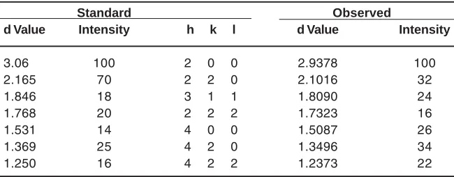
The indexing of the patterns was therefore done by assuming the FCC structure with lattice parameters a = 6.124Å 16. The observed diffraction data is compared with standard ASTM file no. 6.354 and presented in Table -1. The effect of annealing is to increase the peak intensity. The average crystallite size is calculated from the XRD studies by using Scherrer’s relation17. An improvement in grain size from 100 to 400Å.
Surface morphology
Scanning electron micrographs is also shown in Fig. -2. The as grown films is polycrystalline
with crystallite randomly scattered on the surface. The size of crystallite is in the range (100 to 400 Å). Which confirms the film is fine and lustrous film shows the presence of microgrannuals on the complete surface. However large number of granuals have been gathered at some places such as elevations c, d & e black figures of triangular shaped and rectangular shaped have been observed, these regular black figures on the elevated surface shows of presence of voids. It may be conclude that as there is dendraitic growth on the some part of the surface, if the condition is still further improved, the process of evaporation will be able to produce some crystal on the surface during evaporation.
Optical properties
Optical transmission and reflection spectra The reflectance and transmittance spectra of these samples were recorded using Hitachi spectrophotometer model – 330 in the spectral region 200 – 2600 nm. Using these data, the absorption coefficient ‘a’ has been calculated by applying the relation,
α = ln ...(1)
The absorption coefficient can be written in general form as a function of incident photon energy hn as Pankove18,
αhν = A0 (hν-Eg) p ...(2)
where, p has discrete values like 1/2, 3/2, 2 or more depending on whether the transition is direct or
Table - 1: Comparison of standard and observed XRD data (d = 5000A0)
Standard Observed
d Value Intensity h k l d Value Intensity
3.06 100 2 0 0 2.9378 100
2.165 70 2 2 0 2.1016 32
1.846 18 3 1 1 1.8090 24
1.768 20 2 2 2 1.7323 16
1.531 14 4 0 0 1.5087 26
1.369 25 4 2 0 1.3496 34
(200)
(220)
(222)
(311)
(400)
(420)
(422)
Fig.-1 : X-ray diffractogram for Pure PbSe thin film of thickness 5000A0
Fig.- 2 : Scanning Electron Micrograph of PbSe thin film (d = 5000 Å)
indirect and allowed or forbidden. In the direct and allowed cases P=½ where as for the direct but forbidden cases it is 3/2. But for the indirect and allowed case P=2 and for the forbidden cases it will be 3 or more. And the constant Ao is given by
A0 = [e2/neh2m e*] (2mr)
3/2
Eg is the optical band gap, the value of ‘P’ determined the nature of optical transition. The results have been analyzed according to the relation (2). Optical constants, refractive indices and extinction coefficients, have been evaluated from the reflection data and using the relations. Goswami19.
R = ...(3)
and
a = ...(4)
Absorption coefficients have been evaluated using percentage transmittance data as a function of wavelength presented in Fig. -3 for the samples of different thicknesses.
The optical transition observed by different workers is more or less in agreement with one another as far as the gap width of approximately 0.80 eV is concerned. The transmission data have been used to plot the curves of (αhν)2 Vs hν are presented in Fig.- 4. These curves clearly show linearity and by extra polluting gives rise the direct transition band gap.
It is seen that band gap is shifted as a function of thickness. The evaluated values of band gap energies are 0.80, 1.00, 1.32 and 1.36 ev for the samples of thicknesses 200, 1000, 2000 and 3000 Å respectively. It is however difficult to account for the observed band gap shift as a function of thicknesses. The possible causes of observed band gap shift may accounted to one or more of the following mechanisms:
i) Presence of quantum size effect originated by the microstructure nature of the film with average grains sizes less than 300 Å 20-21. ii) Change in stoichiometry due to loss of metal
ion with that treatment which shifts the value of energy gap. Farrow and Jones22. iii) PbSe should show very low values of
electron and hole effective masses (average electron, hole and reduced effective masses are 0.047, 0.041 and 0.022 respectively) for a crystalline size less than Bohrs diameter and increase in effective band gap due to size quantization and blue shifts in photoconductivity spectral response of evaporated PbTe and PbSe were attributed to small crystal size. Dalven23, Sascha Gorer24 had studied quantum size effects in chemically deposited lead selenide films. They reported variation in band gap energies
in the range from 0.55 to 1.55 ev and they showed that a wide range of different optical properties can be obtained with values of Eg ranging from 0.55 to 1.55 ev.
Also the estimation of grain size of PbSe films in the present work (100 – 400) Å which is well within nano-micro, that is quite supports quantized effect of band gap energies in the range 0.50 to 1.55 ev.
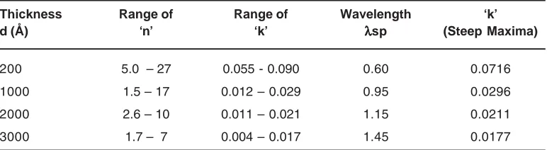
Refractive index and extinction coefficient The variation of refractive indices and extinction coefficients as a function of wavelength is presented in Fig. -5 and Fig. -6 respectively for the thicknesses 1000, 2000, 3000 Å. From these figures it is found that there is remarkable variations in ‘n’ and k as a function of wavelength and strongly depend on thickness of the sample. The variation in ‘n’ is no longer systematic as a function of thicknesses. Also these variation are quite distinguished in two wide wavelength regions namely (0.30-1.50)µ and (1.50-2.60)µ. The study of refractive indices for the different thicknesses reveals the following facts:
i) For the thickness sample of thickness 200 Å. In low wavelength region magnitude of ‘n’ is large and oscillatory in nature. While in high wavelength region ‘n’ value slowly but continuously decreasing. The behavior is similar to reflectance as a function of wavelength.
ii) For the sample of thickness 1000 Å in variation of ‘n’ well defined peaks are observed a broad peak is found in the wavelength range (1.40-2.00)µ.
iii) For the thicker samples of thickness 3000 Å, the variation in ‘n’ initially increases slowly and steadily attains maximum value in low wavelength region, then becomes oscillatory.
Refractive indices varies from 1.5 to 27 while the range of variation of extinction coefficient is from 0.004 to 0.030.This is presented in Table-2. The observed variation in ‘n’ value is theoretically expected. Theoretically refractive indices increased with denser medium. For highly transparent non-absorbing medium ‘n’ is grater than ‘1’. In such case naturally reflectance is very low even less than
h
ννννν
(ev)
Fig.-4 : Variation of (αααααhννννν)² with photon energy for PbSe thin film
5-10 %. While reflectance is more than (50-60) percent ‘n’ values are high and when reflectance approaches to 100 % ‘n’ may be infinity.
According to Table - 2 it is seen that range of ‘n’ value is large for low thickness samples and it is expected. Mathematically this can be explained as the expression for ‘n’ derived and simplified the relation (3) Robinson25.
...(6)
For the extreme case
[(1+R/1-R)2] >> (1+K2) ...(7) For the moderate values of K the above expression becomes,
n+ = 2 (1+R/1-R) and n- = 0
in this case for low value of R, the value of ‘n’ are lower. As R increases and approaches to ‘1’ then n = infinity. This observed variation in ‘n’ is theoretically expected.
In case of extinction coefficient ‘k’ variation for the thinnest sample of 1000 Å is initially there is steep rise in ‘k’ attains maximum value and then steadily increases in high wavelength region, the curve is seemed to be valley shaped. While for the thicker samples of thicknesses 2000 and 3000 Å in low wavelength region ‘k’ values steeply and linearly increases and attains maximum value at particular λsp this specific wavelength seems to be thickness dependent clearly seem from Table - 2.
For all samples of different thicknesses ‘k’ takes value from 0.0055 to 0.09. For the thinnest sample of thickness 200 Å the largest value is in the range 0.09 and 0.05. While for the thicker sample of 3000 Å the range of ‘k’ is 0.0049 to 0.0177.
The comparative study in variation curves of ‘k’ reveals the following facts.
1. If transmittance increases ‘k’ value decreases.
2. If transmittance decreases ‘k’ value increases.
3. If transmittance is constant, there is steep increase in ‘k’ curves.
Table - 2: Optical parameters of PbSe thin films
Thickness Range of Range of Wavelength ‘k’
d (Å) ‘n’ ‘k’ λλλλλsp (Steep Maxima)
200 5.0 – 27 0.055 - 0.090 0.60 0.0716
1000 1.5 – 17 0.012 – 0.029 0.95 0.0296
2000 2.6 – 10 0.011 – 0.021 1.15 0.0211
3000 1.7 – 7 0.004 – 0.017 1.45 0.0177
All the facts are obvious and expected, from basic theory of reflectance, transmittance and absorption. The same can be easily seen from mathematical defining expression of ‘k’ as
k = αλ/4π = 2.303 d log (1/T) λ/4π ...(8) The fact can also be explained on the basis of above expression (8) of ‘k’. The range of wavelength at which transmittance is constant, increase with the thickness of the sample. The above
are reported earlier for PbSe material in thin film form.
Conclusions
Polycrystalline lead selenide films have been deposited on to amorphous glass substrates, as revealed from XRD analysis and evaluated crystallite size ranging from 100 Å to 400 Å only. The lead selenide thin films are stoichiometric in nature with cubic in structure. The dependence of optical parameters of the films on light energy supports the direct characters of the interband transition through an optical band gap in the range
0.8 to 1.36 ev that is thickness dependence. There is remarkable variations in optical constants as a function of wavelength and strongly depend on thickness of the sample. The variation in ‘n’ is no longer systematic as function of thickness.
ACKNOWLEDGEMENTS
The authors are thankful to Prof. Dr. S. R. Chaudhari, Principal B.V. Chavan, Prof. S. A. Patil, Prof. Dr. L.A. Patil, Dr. D. N. Gujarathi, Prof. R.U. Vaidya. The authors are also grateful to Prof. Dr. P P. Patil, Head, Department of Physics, North Maharashtra University, Jalgaon.
1. T. K. Chaudhari, H. N. Acharya and B. B. Nayak, Thin solid films, 83, 169 (1981). 2. D. N. Goryachev, L. G. Paritskii and S. M.
Ryvkin, Sov. Phys. Semicon; 4, 1354 (1971). 3. T. K. Chaudhari, H. N. Acharya and H. N. Bose, Proc. Symp. On. Luminescence and applied phenomenon Khasagpur India (1978). 4. L. P. Biro, R. M. Candea, G. Borodi, A. L.
Darabont, Thin solid films, 165, 303 (1988). 5. Mc. T.J. Mohan and S.N. Jusperson, Appl. Opt.
14, 2750 (1974).
6. R. Marchini and R. Gandi, Appl. Phys. 49 390 (1978).
7. N.N. Salaschehenko, O.N. Fitori, Sov. Phys. Semicond. 13, 1017 (1979).
8. L. P. Biro, A. L. Darabont, P. Fitori., Euro. Phys. Let., 4, 691 (1987).
9. G. Hodes, Albu yaron A., Proc. Electrochem. Soc., 298, 88-14, (1988).
10. R. Valiev, V. Gertsman and O. Kaibysheve, Phys. Status. Solidi, 97, 11K (1986). 11. D.Dadarlat, R.M.Candea, R.Turcu and
L.P.Biro, Phys. Status Solidi A, 108, 637 (1988).
12. G. Hodes, Isr. J. Chem. 33, 95 (1993). 13. J. M. Nedeljkovie, M. T. Nenadovic, O. I. Micic,
J. Phys. Chem., 90, 12 (1986).
REFERENCES
14. A.C.Chang, W.F. Pfeiffer, B. Guillaume, S. Baral, J. Phys, Chem., 94, 4284 (1990). 15. E. H. Sondheimer, Adv. Phys. Lett., 14, 345
(1969) .
16. R. N. Mulik, C. B. Rotti, B. N. More, D. S. Sutrave, 34, 903-907 (1996).
17. N. El. Kadry, A. Ashour, S. A. mahmoud, Thin Solid Films, 269, 112 (1995).
18. J. I. Pankove, Optical processes in semiconductors, prentice-Hall Englewood cliffs NJ (1971).
19. A. Goswami,Thin Film Fandamentals, New Age international Pvt. Ltd. 442 (1996). 20. N. El. Kadry, M. F. Ahmed and K. Abdel Hady,
Thin Solid Films, 274, 120 (1996).
21. F. Cerdeira, I. T. Torriani, P. Mostisuke, V. Lemos and F. Decker, App. Phys. A, 46, 107 (1988). 22. R. F. C. Farrow, G. R. Jones, G. M. Willamns and I. M. Yong, Appl. Phys. Lett. 39, 954 (1981).
23. R. Dalven, Infrared phys., 9, 141 (1969). 24. Sascha Gorer, Aha-Albu-Yaron and Gary
Hodes, J. Phys. Chem., 99, 16443-16448 (1995).