A PROJECT REPORT
ON
Analog Project Title
&
Digital Project Title
SUBMITTED BY
Group Member 1
Group Member 1
Group Member 2
Group Member 2
Group Member 3
Group Member 3
FIFTH SEMESTER
Rizvi College of Engineering
(Off. Carter Road, Bandra (West), Mumbai - 400 050)
DEPARTMENT
OF
ELECTRONICS & TELECOMMUNICATION
ENGINEERING
RIZVI COLLEGE OF ENGINEERING
(Off. Carter Road, Bandra (West), Mumbai - 400 050)
FOR THE FULFILLMENT OF THE PROJECT (TE) ELECTRONIC WORKSHOP (EWS)
A Project Report
on
‘
Analog Project Title
&
Digital Project Title
’submitted by
Group Member Nmae
Under The Guidance Of
PROF. MOHAMMED JUNAID PROF. SADASIVAM.S
DEPARTMENT OF ELECTRONICS ENGINEERING
RIZVI COLLEGE OF ENGINEERING
(Off. Carter Road, Bandra (West), Mumbai - 400 050)
University Of Mumbai
CERTIFICATE
This Is To Certify: Group Member Name
From T.E. EXTC have successfully completed their project “Analog Project Title & Digital Project Title ” and submitted the report as per requirement for the course under the academic year 2012-2013.
___________________ __________________
PROF. MOHD JUNAID EXTERNAL EXAMINER
(PROJECT GUIDE)
___________________ ___________________
PROF. SADASIVAM.S PROF. RAJAN.S.DESHMUKH
PREFACE
__________________________________________________________________
We take an opportunity to present the project report on “Analog Project Title & Digital Project Title”and put before users some useful information about our project.
We have made sincere attempts and taken every care to present this matter in precise and compact form.
We are sure that the information contained in this volume would certainly prove useful for better insight in the scope and dimension of the subject.
ACKNOWLEDGEMENT
LIST OF CONTENTS
__________________________________________________________________
ANALOG PROJECT TITLE
1. Abstract
2. Introduction.
3. Circuit Diagram & Its operation.
4.Simulation in Multisim.
5. Pcb Layout.
a) Real World.
b) Bottom Layout.
6. Components List.
7. Advantages & Disadvantages.
8. Results.
9.Future Scope.
10. Refrences.
DIGITAL PROJECT TITLE
DISTANCE
ABSTRACT
_____________________________________________________________
INTRODUCTION
_____________________________________________________________
Infrared (IR) sensors are widely used as proximity sensors and for obstacle avoidance in robotics. They offer lower cost and faster response times than ultrasonic (US) sensors. However, because of their non-linear behaviour and their dependence on the reflectance of surrounding objects, measurements based on the intensity of the back-scattered IR light are very imprecise for ranging purposes. For this reason, environment maps made with this type of sensor are of poor quality, and IR sensors are almost exclusively used as proximity detectors in mobile robots.
WORKING
_____________________________________________________________
The project mainly consists of four units: an IR sensor unit, an ADC component, a Microprocessor and the LCD module.
CIRCUIT DIAGRAM
LIST OF COMPONENTS & COST ESTIMATION
COMPONENT NAME QUANTITY PRICE (RS)
AT 89C51 1 40 ADC 0804 1 85 IC 7805 1 07 16 X 2 LCD 1 125 6" X 4" General Purpose PCB 1 25
IR Pair 1 10 330 Ω Resistor 1 01 10 kΩ Resistor 3 03 10 kΩ Potentiometer 2 04 150 pF Capacitor 1 01 10 µF Capacitor 1 02 11.0592 MHz Crystal 1 05 Battery Connector 1 03 40 Pin IC Holder 1 05 20 Pin IC Holder 1 05 2 Pin Terminal Block 1 02
TOTAL 323
_____________________________________________________________
ADC 0804 (Analog To Digital Converter)
Features:
Compatible with 8080 Microprocessors.
No zero adjust required
Differential analog voltage inputs
Logic inputs and outputs meet both MOS and TTL voltage level specifications
Works with 2.5V (LM336) Voltage Reference
On-chip clock generator
0V to 5V analog input voltage range with single 5V supply
Easy interface to all microprocessors, or operates ‘stand alone'
Operates ratiometrically or with 5 V dc, 2.5 V dc, or analog span adjusted voltage reference
Description:
has an inbuilt clock which can be used in absence of external clock. A suitable RC circuit is connected between the Clock IN and Clock R pins to use the internal clock.
Pin Connections (Top View):
Pin No Function Name
1 Activates ADC; Active low Chip select 2 Input pin; High to low pulse brings the data from internal registers to
the output pins after conversion Read 3 Input pin; Low to high pulse is given to start the conversion Write 4 Clock Input pin; to give external clock. Clock IN 5 Output pin; Goes low when conversion is complete Interrupt 6 Analog non-inverting input Vin(+) 7 Analog inverting Input; normally ground Vin(-) 8 Ground(0V) Analog Ground 9 Input pin; sets the reference voltage for analog input Vref/2 10 Ground(0V) Digital Ground 11 – 18 8 bit digital output pins D7 - DO
19 Used with Clock IN pin when internal clock source is used Clock R 20 Supply voltage; 5V Vcc
Features:
Compatible with MCS-51 Products
4K Bytes of In-System Reprogrammable Flash Memory
Fully Static Operation: 0 Hz to 24 MHz
Three-level Program Memory Lock
128 x 8-bit Internal RAM
32 Programmable I/O Lines
Two 16-bit Timer/Counters
Six Interrupt Sources
Programmable Serial Channel
Low-power Idle and Power-down Modes
40-pin DIP
Description:
AT89C51 is an 8-bit microcontroller and belongs to Atmel's 8051 family. ATMEL 89C51 has 4KB of Flash programmable and erasable read only memory (PEROM) and 128 bytes of RAM. It can be erased and program to a maximum of 1000 times.
In 40 pin AT89C51, there are four ports designated as P1, P2, P3 and P0. All these ports are 8-bit bi-directional ports, i.e., they can be used as both input and output ports. Except P0 which needs external pull-ups, rest of the ports have internal pull-ups. When 1s are written to these port pins, they are pulled high by the internal pull-ups and can be used as inputs. These ports are also bit addressable and so their bits can also be accessed individually.
Pin Connections (Top View):
Pin No Function Name
1
8 bit input/output port (P1) pins
P1.0
2 P1.1
3 P1.2
4 P1.3
5 P1.4
6 P1.5
7 P1.6
8 P1.7
9 Reset pin; Active high Reset 10 Input (receiver) for serialcommunication RxD 8 bit
input/output port (P3) pins
communication
12 External interrupt 1 Int0 P3.2 13 External interrupt 2 Int1 P3.3 14 Timer1 external input T0 P3.4 15 Timer2 external input T1 P3.5 16 Write to external data memory Write P3.6 17 Read from external data memory Read P3.7 18
Quartz crystal oscillator (up to 24 MHz) Crystal 2 19 Crystal 1 20 Ground (0V) Ground 21
8 bit input/output port (P2) pins /
High-order address bits when interfacing with external memory
P2.0/ A8 22 P2.1/ A9 23 P2.2/ A10 24 P2.3/ A11 25 P2.4/ A12 26 P2.5/ A13 27 P2.6/ A14 28 P2.7/ A15 29 Program store enable; Read from external program memory PSEN 30 Address Latch Enable ALE
Program pulse input during Flash programming Prog 31 External Access Enable; Vcc for internal program executions EA
Programming enable voltage; 12V (during Flash programming) Vpp 32
8 bit input/output port (P0) pins
Low-order address bits when interfacing with external memory
P0.7/ AD7 33 P0.6/ AD6 34 P0.5/ AD5 35 P0.4/ AD4 36 P0.3/ AD3 37 P0.2/ AD2 38 P0.1/ AD1 39 P0.0/ AD0 40 Supply voltage; 5V (up to 6.6V) Vcc
Output Current up to 1A
Output Voltage of 5
Thermal Overload Protection
Short Circuit Protection
Output Transistor Safe Operating Area Protection
Description:
7805 is a voltage regulator integrated circuit. It is a member of 78xx series of fixed linear voltage regulator ICs. The voltage source in a circuit may have fluctuations and would not give the fixed voltage output. The voltage regulator IC maintains the output voltage at a constant value. The xx in 78xx indicates the fixed output voltage it is designed to provide. 7805 provides +5V regulated power supply. Capacitors of suitable values can be connected at input and output pins depending upon the respective voltage levels.
Pin Connections (Front View):
Pin No Function Name
16 x 2 LCD
Features:
5 x 8 dots with cursor
Built-in controller (KS 0066 or Equivalent)
+ 5V power supply (Also available for + 3V)
1/16 duty cycle
B/L to be driven by pin 1, pin 2 or pin 15, pin 16 or A.K (LED)
N.V. optional for + 3V power supply
Description:
Pin Connections (Top View):
Pin No Function Name
1 Ground (0V) Ground 2 Supply voltage; 5V (4.7V – 5.3V) Vcc 3 Contrast adjustment; through a variable resistor VEE
4 Selects command register when low; and data register when high Register Select 5 Low to write to the register; High to read from the register Read/write 6 Sends data to data pins when a high to low pulse is given Enable 7 8-bit data pins DB0
8 DB1
9 DB2
10 DB3
11 DB4
12 DB5
14 DB7 15 Backlight VCC (5V) Led+ 16 Backlight Ground (0V)
Led-MICROCONTROLLER PROGRAMMING
_____________________________________________________________
//Program to interface IR sensor using ADC 0804. Set Vref =1.5v for ADC 0804 #include<reg51.h>
#define port P3 #define adc_input P1 #define dataport P0 #define sec 100 sbit rs = port^0; sbit rw = port^1; sbit e = port^2; sbit wr= port^3; sbit rd= port^4; sbit intr= port^5;
int test_final=0 ,shift=0;
void delay(unsigned int msec ) // Time delay function {
int i ,j ;
}
void lcd_cmd(unsigned char item) // Function to send command to LCD {
dataport = item; rs= 0; rw=0; e=1; delay(1); e=0; return; }
void lcd_data(unsigned char item) // Function to send data to LCD {
dataport = item; rs= 1; rw=0; e=1; delay(1); e=0; return; }
} return; } void convert() { int s; lcd_cmd(0x81); delay(2); lcd_data_string("output:"); s=test_final/100; test_final=test_final%100; lcd_cmd(0x8a); if(s!=0) lcd_data(s+48); else lcd_cmd(0x06); s=test_final/10; test_final=test_final%10; lcd_data(s+48); lcd_data(test_final+48); lcd_data(' '); if(shift>16) { lcd_cmd(0xc0+(shift-1)); lcd_data_string(" "); shift=0;
}
lcd_cmd(0xc0+(shift-1)); lcd_data(' ');
delay(30); }
void main() {
adc_input=0xff;
lcd_cmd(0x38); //2 Line, 5X7 Matrix lcd_cmd(0x0c); //Display On, Cursor Blink delay(2);
lcd_cmd(0x01); // Clear Screen delay(2);
PCB LAYOUT
_____________________________________________________________
ADVANTAGES
_____________________________________________________________
The circuit is simple to design
Low cost
Can be used for measuring small distances with considerable accuracy
Can be used as a proximity sensor or in obstacle detection.
Can be used for assistance parking and similar applications
The device works on 5 to 18 V DC supply
LIMITATIONS
_____________________________________________________________
The behaviour of IR sensor is non linear
Due to dependence on the reflectance of surrounding objects, measurements based on the intensity of the back-scattered IR light are very imprecise for ranging purposes.
The circuit operates on DC and hence requires a separate DC source.
The circuit can be used to measure a very limited distance and hence has limited practical applications
FUTURE SCOPE
_____________________________________________________________
With the development of Sharp IR sensors the circuit can be used for larger distance measurement with better accuracy.
The circuit can be made to operate at standard 230V AC but addition of a transformer and rectifier arrangement.
CONCLUSION
_____________________________________________________________
The circuit, ‘Distance Measurement Using IR Sensor’ was successfully implemented on general purpose PCB. The circuit measures the distance by comparing the change in the resistance of the IR receiver, which depends on the intensity of light falling on it. As this light is reflected by the obstacle, it can be calibrated in terms of the distance and hence distance can be measured. Thus we conclude that the circuit works as per its requirement and design.
REFERENCES
_____________________________________________________________
www.google.com
www.engineersgarage.com
The 8051 Microcontroller - Kenneth J. Ayala Microcontrollers: Architecture, Programming, Interfacing and System Design - Raj Kamal
INTRODUCTION
__________________________________________________________
A counter is a device which stores (and sometimes displays) the number of times a particular event or process has occurred, often in relationship to a clock signal.
DESCRIPTION
__________________________________________________________
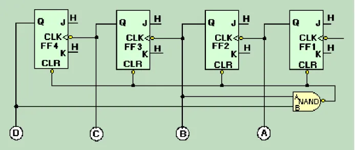
A decade counter is a binary counter that is designed to count to 1010, or 10102. An ordinary
four-stage counter can be easily modified to a decade counter by adding a NAND gate as shown in figure. Notice that FF2 and FF4 provide the inputs to the NAND gate. The NAND gate outputs are connected to the CLR input of each of the FFs.
The counter operates as a normal counter until it reaches a count of 10102, or 1010. At that time,
both inputs to the NAND gate are HIGH, and the output goes LOW. This LOW applied to the CLR input of the FFs causes them to reset to 0. Once the FFs are reset, the count may begin again. The following table shows the binary count and the inputs and outputs of the NAND gate for each count of the decade counter:
BINARY COUNT NAND GATE INPUTS NAND GATE OUTPUT
A B
0000 0 0 1 0001 0 0 1 0010 1 0 1 0011 1 0 1 0100 0 0 1 0101 0 0 1 0110 1 0 1 0111 1 0 1 1000 0 1 1 1001 0 1 1
Changing the inputs to the NAND gate can cause the maximum count to be changed. For instance, if FF4 and FF3 were wired to the NAND gate, the counter would count to 11002 (1210),
and then reset.
SOFTWARE USED
Xilinx Project Navigator is used for writing and synthesizing the VHDL program code. After correction of errors shown during the ‘Synthesize ‘ process, the logic circuit can be simulated and output waveforms can be observed using ModelSim Simulator.
VHDL CODE
__________________________________________________________
library IEEE; --library definition use IEEE.std_logic_1164.all;
use IEEE.std_logic_unsigned.all;
entity Counter is --entity definition port (
clk:in std_logic; reset: in std_logic;
q: out std_logic_vector(3 downto 0) );
end Counter;
architecture Counter of Counter is -- Architecture definition begin
process(clk,reset) -- Process definition
begin
if reset='1' then
qtemp:="0000"; -- Reset asychroniously else
if clk'event and clk='1' then -- Counting state if qtemp<9 then
qtemp:=qtemp+1; -- Counter increase else
qtemp:="0000"; -- Return the zero state end if;
end if;
q<=qtemp; -- Output end if;
end process; -- End Process end Counter; -- End Architecture
OUTPUT WAVEFORMS
ADVANTAGES
We can test circuit and correct errors before programming it into a CPLD or FGPA.
Faster and more accurate as compared to actually connecting circuit on breadboard for testing.
DISADVANTAGES
__________________________________________________________
VHDL is a verbose and complicated programming language.
There are multiple ways of describing the same program in VHDL.
APPLICATIONS
__________________________________________________________
The circuit finds applications in multiplexers and demultiplexers, or wherever a scanning type of behavior is useful.
CONCLUSION
Thus we have studied the VHDL coding of ‘Decade Counter’. The simulation has been carried out successfully and its output waveforms have been verified.
REFERENCES
__________________________________________________________
Notes given in DSD II lectures.
forum.allaboutcircuits.com
free-books-online.org
Digital Logic Design - Godse and Godse
ModelSim user manual
http://www.model.com/
INDEX
__________________________________________________________
A
ADC 0804
i. Features - 13 ii. Description - 13 iii. Pin Connections - 14
B
Battery - 12
C
Capacitor - 12,18
Counter - 15,29,30,31,32,35
Crystal - 12,17,19
D
‘Decade Counter’
i. Description - 29 ii. Waveforms - 33 iii. Advantages - 34
iv. Disadvantages - 34 v. Applications - 34
I
IR Distance Measurement
i. Working - 10
ii. Circuit Diagram - 11 iii. Advantages - 26
iv. Limitations - 26 v. Future Scope - 26
L
LCD
i. Features - 19 ii. Description - 19 iii. Pin Connections - 20
M
Microcontroller
1. AT 89C51
i. Features - 15 ii. Description - 15
iii. Pin Connections - 16,17
ModelSim - 31,35
P
PCB
i. General Purpose - 12,27
PCB Wizard - 25
R
Rectifier - 26
Resistance - 27
S
Sensor - 9,10,21,26,27
T
V
VHDL
i. VHDL Code - 31 ii. Entity - 31
iii. Clk - 31,32 iv. Port - 31
v. Architecture - 32 vi. Waveform - 33
Voltage Regulator
1. KA 7805