FPGA-Based Analog-to-Digital Conversion via
Optimal Duty-Cycle Modulation
Sonfack Gisèle Béatrice1, Mbihi Jean2,*
1
Electronics Department, Faculty of Science, University of Dschang, Dschang, Cameroon
2
Laboratory of Computer Science Engineering and Automation, ENSET, University of Douala, Douala, Cameroon
Abstract
In this paper, a FPGA-based Analog-To-Digital conversion (ADC) architecture via ODCM (optimal duty-cycle modulation), is designed and implemented using software and hardware co-simulation platforms. The software platform consists of Simulink/Xilinx-based system generator blocks in which the ODCM-ADC is implemented, and of Xilinx ISE programing tool for FPGA chips. The hardware platform consists of Zynq 7000 FPGA Kit (25 MHz sampling clock), equipped with an embedded second order FPGA-based digital IIR (infinite impulse response) decimation filter, and with a PC-based JTAG communication cable/connectors. The co-simulation systems, arebuilt and successfully tested for 3 KHz modulating bandwidth. The resulting normalized characteristics are given by: SNR = 49.55 dB, SFDR = 41,19 dB andNoise Floor Range =140 dB. These performance levels obtained under virtual and hardware co-simulation conditions, show
a relevant challenge of ODCM-ADC, compared to most types of oversampling ADC techniques. As a merit, the proposed FPGA-based ADC technique is a novel and relevant ADC architecture for embedded instrumentation systems.
Keywords
Analog-to-digital conversion, Optimal duty-cycle modulation, IIR decimation filter, FPGA, JTAG communication, Virtual and hardware co-simulation, Embedded instrumentation systems1. Introduction
Most artificial and natural signals to be captured for digital processing purposes are analog quantities and consists of a finite frequency spectrum. As an implication, the ADCs (analog-to-digital converters) with a suitable sampling frequency according to Nyquis’s theorem, are widely used in modern instrumentation systems. Although the ADC concept is simple ideally, building an optimal realistic ADC device has been overtime and remains, an intricate and active problem in electronic instrumentation engineering practice. This is due mainly to the fact that each family of ADC devices is designed and implemented for a target application areas, with intrinsic technical and qualitative requirements. As an example, the oversampling ADC architectures, are suitable for instrumentations problems involving servomechanisms, temperature regulation, lighting processes and audio systems [1, 2].
The most popular candidate within this class of oversampling ADC systems is the sigma-delta ADC architecture. Surprisingly, in 2012, a novel oversampling
* Corresponding author: [email protected] (Mbihi Jean)
Published online at http://journal.sapub.org/eee
Copyright©2018The Author(s).PublishedbyScientific&AcademicPublishing This work is licensed under the Creative Commons Attribution International License (CC BY). http://creativecommons.org/licenses/by/4.0/
ADC architecture founded on the DCM (duty-cycle modulation) principle, has been studied and well tested with satisfactory results in [4, 5]. However, the following technological problems were outlined: Use of a PC (personal computer) as the DSP (digital-signal-processing) core for real-time oversampling high frequency on/off modulating signals, unreliability of the PC-based clock required for the oversampling process, and implementation of the digital decimation process as a Visual Basic application program. Given these technological problems, it is worth noting that the limitations related to the DCM-ADC architecture, relies on the PC-based environment used for digital signal processing tasks. Indeed, many studies conducted in most recent papers indicate that, the DCM principle provides numerous relevant technical properties and high quality [6, 7], while numerous intricate weaknesses are hidden behind the popular sigma-delta ADC architecture, e.g., higher structural complexity, higher order n-bit decimation filter for reaching a good accuracy, lack of exact analytical models for rigorous design and analysis purposes, and more. It is worth noting also that, although the DCM principle has also been used satisfactory beyond ADC application areas, e.g., DAC (digital-to-analog converters) [8-11], signal transmission [12, 13], and power electronics [14-16], little attention has been devoted to the ODCM problem studied in [17], under Matlab/Simulink framework.
of an ODCM-ADC architecture (virtually modelled in [17]). The co-simulation results obtained at this development research will be very relevant, for a realistic evaluation of technical requirements when using FPGA-based ODCM-ADC technology in embedded electronic instrumentation systems. The remaining content of the paper is organized in several additional sections. Section 2 deals with a brief recall on the ODCM-ADC architecture. In section 3, the FPGA-Based ODCM-in ADC co-simulation processes are presented. Then, the FPGA-Based ODCM-ADC design is conducted in section 4 from Simulink/Xilinx block sets and also using Xilinx ISE programming tool for FPGA chips. Furthermore, in Section 5, the prototyping FPGA-based ODCM-ADC converter is well tested from software and hardware co-simulation processes, and a sample of relevant results obtained are presented.Finally, the paper is concluded in Section 6.
2. Recall of ODCM-ADC Architecture
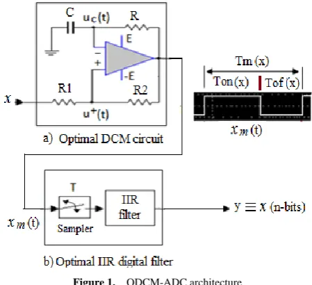
A similar schematic diagram of an ODCM-ADC designed in [1], is recalled in Fig. 1. It consists of two main parts, connected in tandem, i.e., an upstream optimal DCM circuit (see Fig. 1(a)) with modulating input x and DCM output xm(t), and a downstream optimal digital IIR (Infinite
Impulse Response) filter (see in Fig. 1(b)). The optimal DCM circuit is designed according to a set of nonlinear parametric optimization problems with constraints, whereas the optimal IIR filter is synthesized according to the weighted least pth norm specifications.
Figure 1. ODCM-ADC architecture
The optimal parameters of the prototyping ODCM-based ADC system considered in this section are: fs = 25 MHz
(sampling period or Ts = 1/fs = 40 ns equivalently), fs = 3
KHz (Modulating bandwidth), fm(0)=172 KHz (basic
oversampling DCM frequency), E=9 volts (power supply), α* = 0.012366816265686 where α* = R1/(R1+R2) and RC=0.000115510618677 s. It is worth recalling from [17]
that the DCM circuit shown in Fig. 1 is modelled by equation (1), which is quite easy to be implemented in Matlab/Simulink framework.
In addition the z-transfer function of the optimal second order digital IIR decimation filter is given by (2).
(a)
( ) (b
(e ) (c) (d) ) ( ) ( ) ( )
( )
( )
(1
) ( )
( )
( )
( )
1
1
( )
( )
m
m
m
c
uc t
t E
t
t
u
t
x
t
x t
u
t
x
t
E sign
du t
uc t
x
t
dt
x
(1) 22 1 0
2
1 0
0 0.9997782064354348
b z b z b
z 08 2 8.263545624646787e 07 1 1.652709124929357e 08 0 8.2635456 ( ) ( ) ( ) 24646787e 1 1.9997778758936
10 with
m
a
a z a
b b Y z F z X b a z (2)
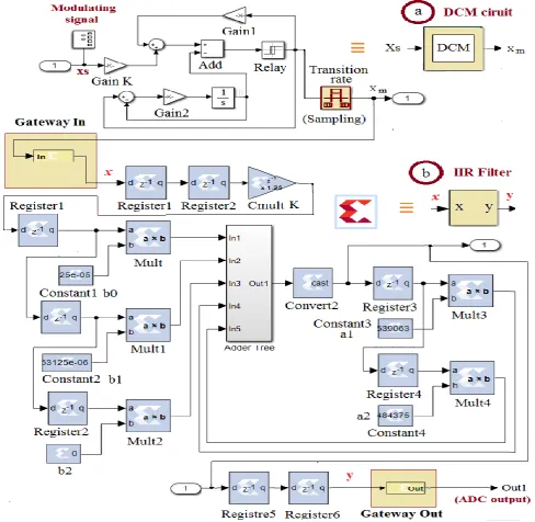
3. FPGA-Based ODCM-ADC Design
The FPGA-Based ODCM-ADC design is conducted under Simulink workspace, according to the schematic diagram presented in Fig. 2. The upstream subsystem shown in Fig. 2(a) is a Simulink-based model of the DCM circuit given by (1), with analog modulating input Xs ≡
x
as in Fig. 1(a), and with a sampled modulation outputx
m.Then, the downstream subsystem presented in Fig. 2(b) is modelled as a digital IIR filter given by (2), which is implemented using visual building resources and configuration panels available in Xilinx System generator framework. The IIR filter is implemented according to the direct form approach. The implemented only required 5 multipliers, 5 registers and an added tree, although the full resolution is maintained across the multipliers and the tree. In addition, the data width cannot grow indefinitely, and thus a quantization block is placed at the output of the adder to reduce the width of the data.
Furthermore, a sample of the corresponding waveforms shown in Fig. 4 is created and well tested also, for the sake of better inspection and validation. The last step of the FPGA-based design process relies on the production of the embedded FPGA file to be executed during software and hardware co-simulation time.
Furthermore, a sample of the corresponding waveforms shown in Fig. 4 is created and well tested also, for the sake of better inspection and validation. The last step of the FPGA-based design process relies on the production of the embedded FPGA file to be executed during software-hardware co-simulation time. From Fig. 4, the following relevant findings could be pointed out:
1) The bits streams of signals involved, are displayed only over a few sampling period for the sake of clarity. The effective simulation time is sufficiently large in order to cover a few periods of the modulating signal.
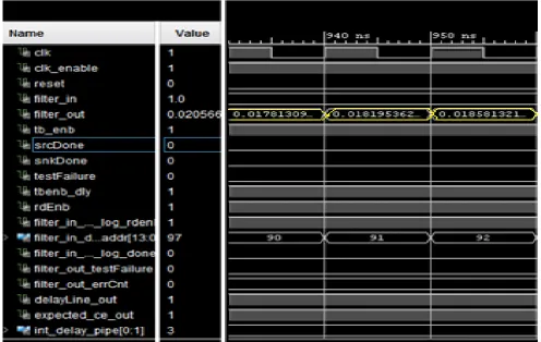
2) The oversampling period of the clock signal named (clk) is T = 950 ns – 940 ns = 10 ns. The waveforms of associated RTL signals are displayed from 931 to 950 ns (time interval).
3) The discrete values of the digital IIR filter response named “filter_out” change over time.
Figure 4. Waveforms of the FPGA-Based ODCM-ADC generated under Xilinx ISE
4. Co-Simulation of the FPGA-Based
ODCM ADC
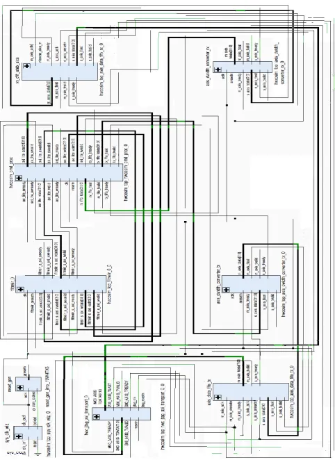
The co-simulation is a powerful modern technique, which is widely used nowadays for rapid testing and evaluating at design time, the predicted and realistic performance of a DSP-based system [18, 19]. Indeed, the co-simulation processes require a PC-based virtual simulation application for DSP (digital signal processing), and a target DSP board equipped with an embedded version of the application code to be simultaneously executed with the virtual application. Both PC and DSP board are connected via an appropriate communication cable/connectors (USB, Ethernet or JTAG). Thus, in a hardware co-simulation context, digital signals involved in a DSP/FPGA chip, are uploaded automatically to the PC-based virtual platform for real-time monitoring.
During a co-simulation session, the virtual simulator and hardware DSP are simultaneously launched and driven under the same operating conditions (input and parameters), while the real-time behavior of the hardware DSP is brought to the virtual simulation environment for the sake of rapid design, performance visualization and evaluation. The co-simulation environment created in this research work for rapid computing and evaluating both predicted and experimental characteristics of the prototyping FPGA-based ODCM-ADC, is presented in Fig. 5.
Figure 5. Hardware Co-Simulation environment
5. Co-Simulation Results
A number of relevant results have been obtained when testing the characteristics of the prototyping FPGA-Based ODCM-ADC in the co-simulation framework. These relevant results are summarized in Fig. 6. Fig. 6(a) shows in the time domain the graphs of 3 signals involved (modu- lating, hwCosim output and Gateway output). It is a challenge to observe in Fig. 6(b) that, even under widely zoomed vision scale, the gap between the graphs of modulating and hwCosim output signals remains negligible. In addition, the values of SNR, SFDR and NOISE FLOOR range computed from Fig. 6(c) and Fig.(d) are 49.55 dB, 41.19 dB and 140 dB respectively.
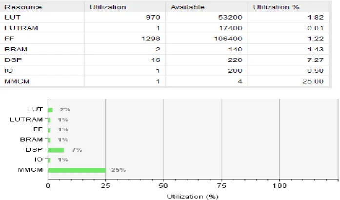
In addition, in Fig. 7, it is worth noting that, the proportion of FPGA resources used for the real-time implementing of the ODCM-ADC architecture is highly low. It is also relevant to evaluate the effective resolution
m(x) of the ODCM-ADC architecture according to the expression (3) as outlined in [8] and [10].
)
(
log
)
(
2x
f
f
x
m
m ech
(3)
with
2 2
2
2 2
2 1 ( )
(1 ) ( 1) m
f x
x E
R C Log
x E
(4)
In (4), the parameters R, C, α = R1/(R1+R2) and E, are those of the DCM circuit in Fig. 1(a), whereas fech and fm(x) stand for the sampling frequency and the DCM frequency respectively, given a modulating input x. It is obvious that (3) is minimum if fm(x) is maximum. Then, following convexity Theorems (see [17] for statement and demonstration), (4) is maximal if x = 0, in which case fm(0) is given by:
(5)
Figure 6. Summary of a sample of Co-simulation results obtained
1 (0)
1 2 R C
1
m
f
Log
Figure 7. Proportion of FPGA resources used for the implementation of ODCM-ADC/ In this case, the minimum value of (3) is given by (6):
2
(0) log
(0)
ech
m
f m
f
(6)
As a relevant implication arising from (6), for a fixed modulating bandwidth, an increase in the oversampling frequency fech is a simple means to increase the ENOB (effective number of bits) of the proposed FPGA-based ODCM-ADC architecture.
In this paper, the optimal parameters used and recalled in section II are given as follows: fech = 25 MHz, RC = τ = 0.000115510618677 s, α* = 0.012366816265686, then fm(0)
=172 KHz and the resulting ENOB (effective number of bits) is 7.1554 bits. Since the advances on today’s FPGA technology lays beyond 500 MHz [20] and even 1.5 GHz of clock frequency [21], the application areas of the FPGA-based ODCM-ADC architecture might rapidly grow over time. However, compared to the technical behavior of most popular candidates operating today within the class of oversampling ADC architectures [22-26], these levels of performance provided by the FPGA-based ODCM-ADC, might be a great challenge under the same operating conditions (modulating bandwidth, sampling frequency, single stage DCM interface, second-order digital decimation filter, no external modulation clock, and more). As a relevant finding, the proposed FPGA-based ODCM-ADC is relevant for embedded instrumentation systems.
6. Conclusions
This paper presents the design and FPGA-based implementation, as well as the hardware co-simulation of the proposed ODCM-Based ADC. The design and co-simulation have been sussesfuly implemented on a target Xilinx ZYNQ 7000 FPGA memory kit. It is worth noting
that the ODCM-based ADC owes its low implementation cost and high quality (stability, accuracy and robustness) to both the harware simplicity and the topological relevance (negative and positive feedback loop) of its interfacing DCM circuit. As a relevant mayor finding, the new FPGA-based ODCM-ADC presented in this paper, might be used as a new potential architectural solution for embedded instrumentation systems.
REFERENCES
[1] G. Eason, N. Doley and A. Kornfeld, “Comparison of Sigma-Delta converter circuit architectures in digital CMOS technology,” Journal of circuits, systems ans computers”, © World scientific publishing company vol. 14, No 3, pp. 515-532, 2005.
[2] A. K. Dewangan, N. Chakraborty, S. Shukla, V. Yadu, “PWM based automatic closed loop speed control of DC motors,” International Journal of engineering trends and technology”, Vol. 3, Issue 2, pp. 110-112, 2012.
[3] J. Holtz, “Pulse width modulation - A survey, ” IEEE transactions on industrial electronics, vol. 39, no. . 5, pp. 410-420, December, 1992.
[4] J. Mbihi, F. Ndjali Beng, M. Kom and L. Nneme Nneme. “A novel analog-to-digital conversion technique using nonlinear duty-cycle modulation,” International Journal of electronics and computer science engineering, 1(3), pp.818-825, 2012 [5] J. Mbihi and L. Nneme Nneme, “A Multi-Channel
Analog-To-Digital Conversion Technique Using Parallel Duty-Cycle Modulation,” International Journal of Electronics and Computer Science Engineering, Vol 1, No 3, pp. 826–833, 2012.
[7] B. Moffo Lonla, J. Mbihi, L. Nneme Nneme, “Low Cost and High Quality Duty–Cycle Modulation Scheme and Applications,” International Journal of Electrical, Computer, Energetic, Electronic and communication Engineering. Vol 8, No 3, pp. 82–88, 2014.
[8] B. Moffo Lonla, J. Mbihi, L. Nneme Nneme and M. Kom. “A Novel Digital–to–Analog Conversion Technique using Duty-Cycle Modulation,”. International Journal of Circuits, Systems and Signal processing, Vol 7, No 1, pp 42–49-8, 2013.
[9] Moffo Lonla B., Mbihi J. A, “Nouvelle technique de conversion N/A des signaux par modulation numérique en rapport cyclique et applications en instrumentation,” Ph/D thesis, ENSET, University of Douala, July 2016.
[10] B. Moffo Lonla and J. Mbihi. “Novel Digital Duty–Cycle Modulation Scheme for FPGA-Based Digital-to-Analog Conversion,” IEEE Transaction on circuits and system II, Vol 62, No 6, pp. 543–547, 2015.
[11] B. Moffo Lonla, J. Mbihi and L. Nneme Nneme, “FPGA-based Multichannel Digital Duty-cycle modulation and Application to simultaneous generation of Analog Signals,”, Journal of Electronic Design Technology, Vol. 8, Issue 21, pp. 23-35, 2017.
[12] L. Nneme Nneme and J. Mbihi. “Modeling and Simulation of a New Duty–Cycle Modulation Scheme for Signal Transmission System,” American Journal of Electrical and Electronic Engineering Vol 2, No 3, 82-87, 2014.
[13] J. Mbihi, Charles-Hubert KOM and Leandre Nneme Nneme, “A suboptimal nonlinear duty-cycle modulation scheme,” Journal of Electronic Design technology, Vol. 7, Issue 1, pp. 22-31, 2016.
[14] J. Mbihi an L. Nneme Nneme, “A novel control scheme for power Buck converter using duty-cycle modulation,” International Journal of Electronics, Vol. 5, No 4/3, pp. 185-199, 2013.
[15] Y. P. Dangwe Soulemanou, J. Mbihi, H. Djala, J. Effa, “Virtual digital control scheme for duty-cycle modulation Boost converter,”Journal of computer science and control systems, Vol 10, No 2, pp. 22-27, 2017.
[16] J. Mbihi, “Dynamic modelling and virtual simulation of digital duty-cycle modulation control drives,” International Journal of Electrical, computer, energetic, electronics and communication engineering, © WASET (World Academic of Science, Engineering and Technology), Vol 11, No 4, pp. 472-477, 2017.
[17] G. Sonfack, J. Mbihi and B. Lonla Moffo, “Optimal Duty-Cycle Modulation Scheme for Analog-To-Digital Conversion Systems”, International Journal of Electrical, computer, energetic, electronics and communication engineering,” © WASET (World Academic of Science, Engineering and Technology), vol. 123, No 3, pp. 348 – 354, March, 2017.
[18] R-L. Chung and P-H. Chang, “Hardware-software co-simulation of downlink LTE-Based Transceiver”, Proceedings of the International MultiConference of Engineers and Computer Scientists,” Vol 2, March 13 - 15, Hong Kong, 2013.
[19] P. R. Kolankar and V. Swati Sakhare, “FPGA Implementation of QPSK modulator by using Hardware Co-simulation,” International Journal of Engineering Research and Development, Vol 10, pp. 86-93, April 2014. [20] R.-D. Albu and E. C. Gordan, “FPGA design and
implementation of a rangefinder”, Journal of electrical and electronic engineering, © Academy of Romanian scientists, Vol 10, No 2, pp. 05-13, October 2017.
[21] Pentek, “Dual 2 GHz, 10-bit A/D with Virtex-II Pro FPGA”,
https://www.pentek.com/, consulted on March, 03, 2018. [22] M. Faghani, M. Binti Isa and N. M. Hamidan, “Integration of
Sigma-delta ADC with sinc filter on FPGA,” Journal of engineering and applied science, Vol 10, No 2, pp. 16-21, 2015.
[23] S. M. Rabiul Islam and A. F. M. Nokib Uddin, “FPGA based sigma-delta modulator design for biomedical application using Verilog HDL,” Global Journal of researches in engineering - Electrical and electronic engineering, Vol 11, No 7, pp. 01-06, December 2011.
[24] S. K. Maity and H. Sekhar Das, “FPGA-based hardware efficient digital filter for Sigma-delta ADC, ” International Journal of soft computing and engineering, Vol 1, No 6, pp. 129-133, January 2012.
[25] P. A Uchagaonkar, S. A. Shinde, V. V. Paul and R.K. Kamar, “FPGA-Based Sigma-Delta analog to digital converter,” International Journal of electronics and computer science engineering, pp. 508-513, January 2013.