https://doi.org/10.3926/jiem.2765
Application of Fuzzy Integrated FMEA with Product Lifetime Consideration
for New Product Development in Flexible Electronics Industry
Kelvin P.L. Pun1,2 , Jason Rotanson2 , Chee-Wah Cheung2 , Alan H.S. Chan1 1Department of SEEM, City University of Hong Kong (Hong Kong)
2Compass Technology Co Ltd (Hong Kong)
[email protected], [email protected], [email protected], [email protected]
Received: October 2018 Accepted: January 2019
Abstract:
Purpose: the aim of this paper is to minimize the risks of new product development and shorten time-to-market, particularly for high-tech enterprise where the complexity of the product generates vast amount of failure mode.
Design/methodology/approach:first, the concept of Critical Consideration Factor (CCF) is introduced based on product-specific technical characteristics, expected lifetime, and yield requirement to identify and prioritize the critical failure mode in the subsequent Failure Mode and Effect Analysis (FMEA), followed by process characterization on the high-risk failure mode and Critical Parameter Management (CPM) practice to realize a robust mass production system of the developed technology. The application on the development of advanced flexible substrate and surface finishes fabrication technique is presented.
Findings: through the proposed methodology, the risk level of each potential failure mode can be accurately quantified to identify the critical variables. With process characterization, reliability of the product is ensured. Consequently, significant reduction in development resources and time-to-market can be achieved.
Practical implications: the development strategy allows high tech enterprises to achieve a balanced ecosystem in which value created through adaption of new technology/product can be thoroughly captured through commercialization in a timely manner with no field failure.
Originality/value: the proposed development strategy utilizes a unique approach with thorough considerations that enables high tech enterprise to deliver new product with rapid time-to-market without sacrificing product lifetime reliability, which is key to achieve competitive advantage in the highly dynamic market.
Keywords: new product development, risk management, failure mode and effect analysis, critical parameter management, advanced manufacturing, industry 4.0
To cite this article:
1. Introduction
1.1. New Product Development
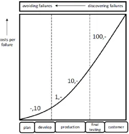
To remain sustainable and profitable, high tech enterprises face multiple challenges in competitive business environments and rapid changes in market demand. One of the key success factors is continuous investment in R&D to create value by commercializing technology into products, setting industry standards, and effectively deterring the entry of rivals (Zahra, 1996). With ever increasing customer expectations, time becomes the critical factor in the development of new technology. Manufacturers are required to achieve short development cycles and consequently time-to-market, while simultaneously offering cost advantages and scalability. Opportunities from NPD also incur huge risks, in which unpredictable obstacles can arise during mass production that lead to unstable yield loss and impede product commercialization. Managing NPD is a vital and challenging process, as it involves extensive financial and human resources (Bhuiyan, 2011). In fact, a considerable number of products never make it to the market, with a failure rate of 25% to 45% (Mosley, 1994; Crawford, 1987). Avoiding failure is paramount in the development of technical products. The earlier the failure detection, the more economic loss can be avoided (Figure 1) and the faster commercialization can be achieved (Würtenberger, Kloberdanz, Lotz & Von Ahsen, 2014). In addition to the cost, commercialized products that experience field failure during their product lifetime will negatively affect customer experience, not to mention possible liability issue. Therefore, solving these unforeseeable problems is critical to achieve successful technology transfer. Indeed, organizations need to employ a multi-dimensional development strategy to ensure that the value created is in equilibrium with the value captured (Rajan, 2016).
Figure 1. Cost per failure that increase logarithmically at different development stage (Würtenberger et al., 2014)
Doğan and Cebeci (2016) integrated the use of QFD to generate FMEA based on customer requirement in NPD process. These studies, despite being able to detect possible risks beforehand, do not ensure a robust system that is ready for mass production while taking into account product lifetime reliability. Natarajan, Senthil, Devadasan, Mohan and Sivaram (2013) implemented quality and reliability on to new product development process, however the methodology presented is not quantitative as it focuses on systematically achieving certain milestone on the product development. Moreover, methodology in traditional FMEA is highly debatable due to the subjective rating as well as questionable weighting and calculation formula. Various methods have been proposed to improve FMEA such as using grey relational analysis and fuzzy logic based on safety, quality, and cost (Baynal, Sari & Akpinar, 2018; Banduka, Tadić, Mačužić and Crnjac, 2018). Therefore, there is a need for novel development strategy based on FMEA that takes into account product quality & reliability from the technical aspect through quantitative analysis to intelligently manage and optimize development resources to reduce development time.
1.2. The Flexible Electronics Industry
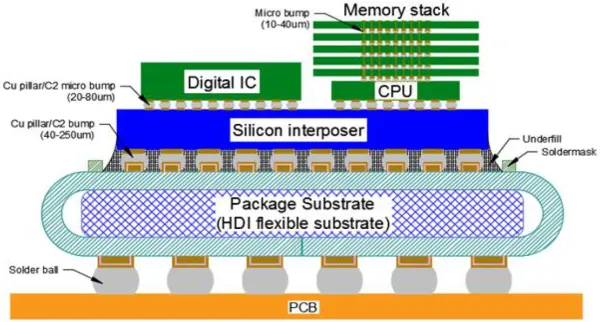
Increasing demand for advanced electronic products with a smaller form factor, multi-functionality, higher performance, and lower overall cost has driven the semiconductor industry to continuously innovate emerging advanced packaging technologies using flexible substrates. The electronic packaging field constitutes a highly sophisticated area that necessitates specific expertise on numerous levels. Choosing the optimal process equipment and materials, combined with innovative design solutions that address thermal, mechanical, and electrical issues will be the key success factors. Figure 2 shows the construction of an advanced electronic package with heterogeneous integration. From top to bottom, the package consists of die (integrated circuit/ IC)/component, IC level interconnect, package level interconnect (1st level), substrate, board level interconnect (2nd level), and the main board itself.
Figure 2. Heterogeneous integration in an advanced electronic package (Pun, Islam, Rotanson, Cheung & Chan, 2018a)
OLED/AMOLED, LCD/TFT displays, smart wearables, medical imaging, and hyperconnected cloud (HyCC) for the internet of things (IoTs). However, integration of more components and material interfaces on advanced package configurations, such as system-in-package (SiP), package-on-package (PoP), and 3D IC integration modules will increase potential failure modes in an exponential manner. These failure modes (especially highly critical ones) must be eliminated early during the development stage, as conducting failure analysis after product commercialization involves another set of huge resources, and often necessitates design changes and engineering change notices (ECN) on many levels due to system complexity. Furthermore, encountered field failures will incur major losses for enterprises in terms of liability, cost, reputation, etc. Therefore, product lifetime performance must constitute a top priority.
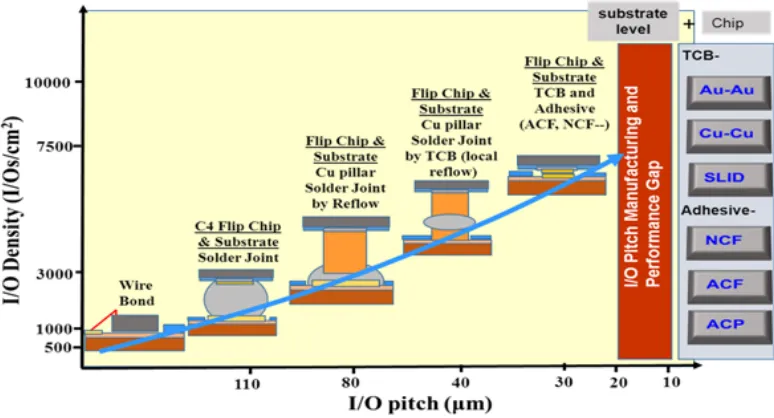
Figure 3. Trend of high-density interconnect (HDI) to support advanced package development
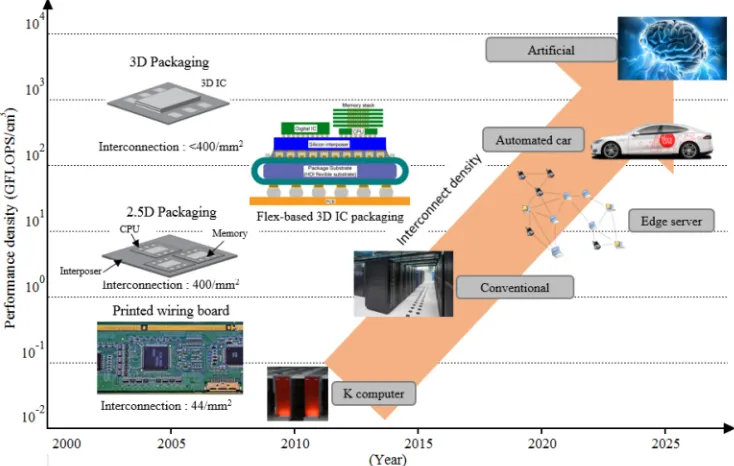
With the demanding product features, along with the rapid change of trend in electronics industry (Figure 4), market research is essential to ensure new product development process is targeting the relevant market segment that benefits both the consumer and organizations. Based on these emerging market trends, three main fields are identified:
1. Display market: Future display modules are also moving towards the integration of display driver IC
and touch controller IC, which benefits design, manufacturing, size reduction, and performance (Synaptics, 2014). This integration means that more functionalities can be incorporated into a single IC, which also requires a COF (Chip-on-film) with an increasingly finer pitch. Expected product lifetime: <5 years.
2. Medical devices market: The medical field demands high performance reliability and ultra-compact
module integration using system in package (SiP) and package on package (PoP) which involve multiple assembly processes. Such configurations necessitate advanced packaging solutions, in terms of interconnect density, pitch, and substrate line/space scalability. Expected product lifetime: 10-15 years.
3. Hyperconnected Cloud Computing (HyCC): In the coming IoTs (Internet of Things) era, all kinds
Figure 4. Device packaging technology for servers (Aoki, 2017)
1.3. Proposed State-of-the-Art Technology
Taking the existing technical challenges involved in the electronic packaging requirement in emerging products into account, the following technologies related to flexible substrate are developed:
1. Flexible circuit fabrication with Fully Additive Process (FAP): The substrate is an integral part of
packaging, as it serves as the backbone of electronic devices by interconnecting all components mechanically and electrically. A flexible substrate is typically fabricated by a subtractive or semi-additive process (SAP or MSAP, respectively), which possesses limitations on meeting circuit density below 20 um pitch, which limit package miniaturization. A fully additive process (FAP) has been developed and proven to outperform the conventional process in terms of functional performance and overall process steps/cost.
2. Advanced Surface Finishing with Electroless Ni/Electroless Pd/Immersion Au (ENEPIG):
Surface finish plays a vital role in the final steps of substrate fabrication since it not only protects the exposed copper circuit, but also affects the final interconnection performance due to the interfacial reaction of the surface finishing material during the assembly process. ENEPIG is a promising solution to address the reliability and miniaturization requirement of future electronics due to the low overall thickness and electroless plating method that simplifies process steps.
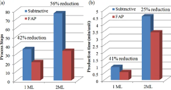
List of technical features to be addressed in the development of the two technologies is shown in Figure 5. Combining these two technologies in a reel-to-reel form with the latest interconnect technology constitutes a unique approach to realize an advanced electronic packaging system while achieving considerable process steps and cycle time reduction, as shown in a comparative study of our production line (Figure 6). These two technologies are promising to support advanced interconnect technologies, including direct diffusion bonding and copper pillar soldering (1st level interconnect) and low temperature soldering (2nd level interconnect).
Figure 5. Features of the proposed state-of-the-art technology in fulfilling the latest product technical requirement
Figure 6. (a) Process steps reduction; (b) Production time reduction with the proposed development technology as compared to conventional process
2. Proposed NPD Methodology
Figure 7.Factors affecting competitive advantage of high-tech enterprises
Figure 8. Overview of the development tools methodology
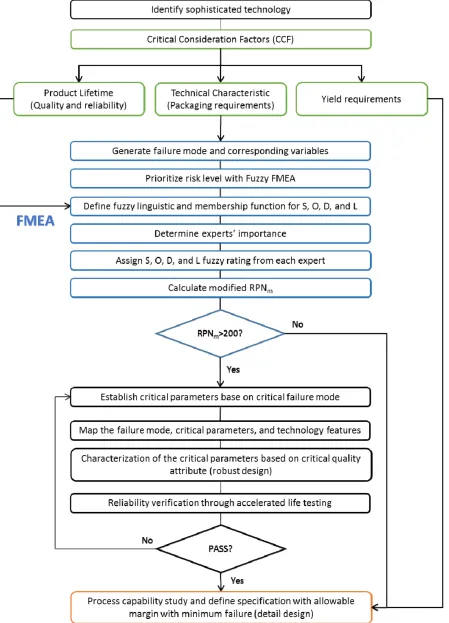
From the technical characteristics, all potential failure modes, with causative variables and quality attributes, can be identified. Risk priority can then be determined by utilizing the FMEA method. The complexity of emerging products generates large amounts of failure modes that must be accurately prioritized. Fuzzy logic is one of the most powerful tools in artificial intelligence (AI) to improve decision making concerning uncertain phenomenon, which is suitable to minimize the subjectivity of traditional FMEA. In this paper, fuzzy logic is used on the FMEA by integrating the new element of product lifetime (L) in addition to conventional severity (S), occurrence (O), and detectability (D) to calculate the modified risk priority number (RPNm). Next, by setting a
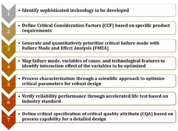
certain threshold, the failure mode can be classified based on risk level. As critical failure modes constitute the major concern that might hinder the adoption of new technology for mass production, their corresponding causative variables are then set to be the critical process parameter (CPP). The CPP needs to be managed through extensive process characterization in a scientific manner for robust design, and corresponding specifications need to be defined for a detailed design. Here, it is important to understand the relationship of the variables in the failure mode, as well as the correlated key technology features. Through critical parameter management (CPM), a robust system can be established by consistently employing the optimized parameters that fulfil the critical quality attribute (CQA) and reliability requirement throughout mass production. The result will also need to be well documented in an interconnected database network. Furthermore, with the advancement of Industry 4.0, a cyber-physical system (CPS) that connects digital and physical workflow allows for effective implementation of the robust system. This leads to realization of smart products that possess a high degree of autonomy in terms of its own operation, coordination and diagnosis, as the product has information/knowledge to understand itself, its environment, and its users throughout the lifecycle (Nunes, Pereira & Alves, 2017). With the proposed strategy, efficient implementation of new technology with minimum risk can be achieved to precisely fulfil the latest market niche in a timely fashion.
3. Implementation on the Proposed Technology
This section presents the implementation of the development tools in the development of the advanced substrate fabrication and surface finishing technology.
3.1. Critical Consideration Factor (CCF) Identification and Fuzzy Failure Mode and Effect Analysis (FMEA)
Figure 10 shows the flowchart of the CCF integration to FMEA, as well as CPM. To determine CCF, product requirements have to be fully understood according to the application by identifying the three elements presented in Figure 9. First, the technical characteristics must be defined based on the packaging requirements, i.e., the material, process, and design involved on each of the interfaces in the packaging configuration. Second, the expected lifetime of the product has to be identified to determine the necessary quality and reliability level, as shown in Figure 11 (Lee, Bieler, Kim & Ma, 2015). In this paper, high reliability products are targeted based on market needs. Finally, the yield requirement, which depends on the particular market and business model, have to be taken into account when determining the specifications. Defining CCF based on this can make a great difference in allocating development resources efficiently. With appropriate considerations, an efficient, yet accurate, development process can be achieved. First, the variables with resulting failure modes are determined based on the technical characteristics of the proposed technology. This is represented in the diagram in Figure 12.
14, respectively. Concerning the lifetime variable, the assignment is adjustable depending on the target product requirement. Here, the membership degree increases with lifetime, as we are targeting high reliability electronic products.
Figure 11. Quality and reliability considerations for consumer electronics and high reliability electronics (Lee, 2015)
Figure 12.Factors and failure mode of the proposed technology development
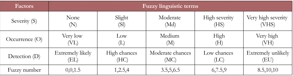
Factors Fuzzy linguistic terms
Severity (S) None(N) Slight(Sl) Moderate (Md) High severity (HS) Very high severity (VHS)
Occurrence (O) Very low (VL) Low(L) Medium (M) High(H) Very high (VH)
Detection (D) Extremely likely(EL) High chances (HC) Moderate chances(MC) Low chances (LC) Extremely unlikely(EU)
Fuzzy number 0,0,1.5 1,2.5,4 3.5,5,6.5 6,7.5,9 8.5,10,10
Figure 13. Fuzzy linguistic membership function for severity, occurrence, and detection (Kirkire, Rane & Jadhav, 2015)
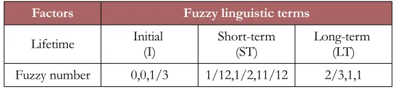
Factors Fuzzy linguistic terms
Lifetime Initial (I) Short-term(ST) Long-term (LT)
Fuzzy number 0,0,1/3 1/12,1/2,11/12 2/3,1,1 Table 2. Fuzzy linguistic variable assignment for L
Figure 14. Fuzzy linguistic membership function for lifetime
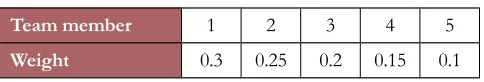
The weight of experts that reflects their influence on the risk evaluation is then calculated using the following equation:
w
tmk=
E
tmk∑
k=1
n
E
tmk (1)Team member 1 2 3 4 5
Weight 0.3 0.25 0.2 0.15 0.1
Table 3. Weight assignment of each team member
Assignment of the fuzzy linguistic variable is shown in Appendix B. The fuzzy linguistic terms are calculated based on the methodology developed by Kirkire et al (2015), as shown in the following:
Sijn=(SLnij, SMnij,SUijn), Snij∈T , where
0≤SLijn≤SMijn≤SUnij≤10
(2)
Oij n=(OL
ij n, OM
ij n, OU
ij n),O
ij n∈T ,
where
0≤OLijn≤OM ij n≤OU
ij
n≤10 (3)
Dijn=(DL ij
n, DMijn, DU ij
n), Dijn∈T ,
where
0≤DLnij≤DMijn≤DUijn≤10
(4)
Lijn=(L Lijn, LMijn, LUnij), Lijn∈S , where
0≤L Lij n
≤LMijn≤LUij n
≤1
(5)
Sij=Sij1x Wtm1+S2ijx Wtm2+...+Sijnx Wtmn (6)
Oij=Oij1x Wtm1+Oij2x Wtm2+...+Oijnx Wtmn (7)
Dij=Dij1x Wtm1+Dij2x Wtm2+...+Dijnx Wtmn (8)
Lij=Lij 1
x Wtm1+Lij 2
x Wtm2+...+Lij n
x Wtmn (9)
WhereSijn ,Oijn , Dijn andLijn are the severity, occurrence, detectability, and lifetime, respectively, assigned by n experts for interface of i and risk of j; Sijn∈T , Oijn∈T , Dijn∈T and Lijn∈S are the membership function of the triangular fuzzy number Sij ,Oij , Dijrespectively; Lij is the severity, occurrence, detectability, and lifetime value of experts’ opinion for interface i and risk j; Wtmk is the weight of kth team member; and n is the number of experts. Fuzzy numbers on the probability of S, O, D, and L are aggregated by equations (6)-(9) (Lin, Liu, Liu & Wang, 2013). Next, these fuzzy numbers are defuzzified into numerical values by the following equation:
DSk=
[(SUk−SLk)+(SMk−SLk)]
3 +SLk∀k (10)
DOk=
[(OUk−OLk)+(OMk−OLk)]
DDk=
[(DUk−DLk)+(DMk−DLk)]
3 +DLk∀k (12)
DLk=
[(LUk−L Lk)+(LMk−L Lk)]
3 +L Lk∀k (13)
Where DSk, DOk, DDk and DLk are the defuzzified severity, occurrence, detectability, and lifetime fuzzy sets, respectively. Finally, the modified RPN can be calculated using the equation below:
RPNm = DSk x DOk x DDk x DLk (14)
Based on this RPNm, the failure mode is classified as follows: above 200 is set to be critical risk; between 100 to 200 is set to be moderate risk; between 50 to 100 is set to be low risk; and below 50 is set to be negligible risk. In this study, 19 critical failure modes have been identified out of a total of 61 failure modes (Figure 15).
Figure 15. Failure mode RPN in the development of advanced flexible substrate
3.2. Process Characterization and Critical Parameter Management
Figure 16. Correlation between high priority failure mode, critical parameter, and technology development features
Figure 17. Process capability of trace top/bottom ratio (a) robust design with CPM and (b) uncontrolled system design with
occurrence of failure
Technological Features
Fuzzy FMEA Sorted Failure
Mode
Process Characterization Reliability Verification(PASSED)
Parameter StudiedRange OptimumValue Parameter Target Condition Method/Tools
Metallurgy diffusion bond compatible (Pun, Dhaka, Cheung & Chan, 2017a)
Interfacial void Temperature 180-340°C 320°C
Shear strength >50 MPa TemperatureHumidity Storage (60°C/60% RH for 1000 h) FIB cross-section Insufficient
diffusion Pressure 55-175 Mpa 155 Mpa Insufficient/
skip contact Time 1-11 s 10 s
Exposed copper Ni Thickness 1-3 um 3.0 um Trace peeled off(peel test failure
mode) 100%
Metal residue Pd Thickness 0.05-0.4 um 0.4 um misalignmentBonding <2 um Thermal Shock Test
(125°C to -40°C for 1000 cycles)
Electrical test Dendrite growth Au Thickness 0.04-0.07um 0.04 um
Void formation Fully shrunk Oxidation roughness (Ra)Surface 90-150 nm <100 nm
Cu pillar micro bump(C2) compatible (Pun, Islam, Cheung & Chan, 2017b)
IMCs growth
Ni Thickness 1-1.3 um 1 um
Overall IMCs thickness after
isothermal aging <4 um
Thermal aging 150°C
for 1000 h
SEM/EDX & cross-sectioning Exposed copper
Metal residue Pd Thickness 0.05-0.4 um 0.05-0.2 um Critical IMCsformed (Pd,Cu,Au)Sn4
(Cu,Ni)6Sn5
Dendrite growth
Au Thickness 0.04-0.2 um 0.04-0.07 um
Die peel failure
interface Within solderside
Oxidation Growth rateconstant of IMCs <2x10
-14 cm2/s
Low temperature solder compatible (Sn-Bi-Ag) (Pun et al., 2018a)
IMCs growth Ni Thickness 1-4 um 1-1.5 um Shear strength >1000 gf
Extended reflow at 175°C for 120 mins SEM/EDX & cross-sectioning Exposed copper Pd Thickness 0.04-0.7 0.15-0.2 um
Failure mode 100% solder oninterface Metal residue
Au Thickness 0.03-0.05um 0.04 um
Dendrite growth Critical IMCsformed (Ni,Cu)3Sn4
Oxidation Ni consumption 0.009 um/minreflow
Base film modification and nano-level chemical bonding (Pun, Ali, Kohtoku, Cheung, Chan & Wong, 2018b)
Trace adhesion failure
Modifier concentration
(on polyimide) 15-40 mL/L 25 mL/L
PAA layer
thickness <5 nm
Temperature Humidity Storage (85°/85% RH) TEM inspection
Peel test failure
Carboxyl
bonding >3%
Low Temperature
Storage (-40°C for 500
h)
XPS analysis
Amide bonding >6%
Hight Temperature Storage (150°C
for 500h)
Technological Features
Fuzzy FMEA Sorted Failure
Mode
Process Characterization Reliability Verification(PASSED)
Parameter StudiedRange OptimumValue Parameter Target Condition Method/Tools
Moisture Senstivity Level
3 (-60°C to 60°C for 48 h and 3x
reflow at 254°C) Porous surface Peel strength >0.6 kN/m
Signal delay/ propagation
Ni-P layer
coverage 100% Thermal ShockTest (125°C to -40°C for 500
cycles)
SEM inspection Thickness 100-110 nm
High speed electrolytic pattern plating
(Pun et al., 2018b)
Bending endurance failure
Plating rate um/min0.2-0.6 0.2 um/min Grain size >2 um
Heat treatment (200°C and 300°C for
24 h)
SIM cross-sectioning Current density 1-2.5 ASD 1 ASD enduranceBending >35 cycles
Over-deformed trace
Temperature 315-375ºC 345ºC Strain <0.2
Pressure 120-160MPa 140 MPa microstructureInterfacial of Au-Au
Interlocking nano-twin
structure
Isotropic etching (Pun et al., 2018b)
Conductor undercut
Etching time 60-75 s 75 s
Insulation
resistance >105 Ohms
Temperature Humidity Bias (85°C/85% RH/20 VDC) Insulation resistance measurement Insulation resistance after thermal humidity bias
>105 Ohms
Over-etching
Standard deviation of
impedance <1 T/B ratio ~1
Seed layer residue
Cpk of T/B
ratio >1.33 Line/space
scalability <8/8 um Cpk of
line/space >1.33 Signal
performance (Pun et al., 2018b)
Signal delay/ propagation
Interface
roughness (Rq) 40-320 nm 40-70 nm
Conductor loss
factor (Ksr) <1.05 N/A
Table 5. Critical parameter optimization based on the critical quality attribute criteria
Cupper = (A+B) + M (15)
Clower = (A-B) - M (16)
│Cupper – Yupper │≥ σ, Clowerr – Ylower ≥ σ (17)
where A is the optimal value from process characterization; Yupperand Ylower are the upper and lower limit before the occurrence of failure, respectively; B is half of the target sigma level; Cupper and Clower are the lower and upper specification, respectively; and M is the margin allowed for the specification as shown in Figure 18. Allowing this margin is crucial so that room for error exists, which means that even though the process is outside of the sigma level standard, failure will still not occur. Obviously, the margin should be adjusted depending on the process capability, targeted sigma level, and yield requirement.
Finally, the robust system has to be followed up by appropriate operational management practices so that the optimum design can be carried out consistently throughout production. Critical parameter management is one excellent practice to assure that system robustness is maintained through detail specification, proper documentation, and in line quality control (QC) (Clausing, Frey & Systems Engineering, 2010). With a manufacturing and production implementation plan for the critical parameters, quality evaluation, and changes in the control plan, the value created through robust design can be delivered to the customer.
4. Conclusion
Enabling robust technology transfer with minimum time-to-market constitutes the key to enhance business competitiveness in high tech enterprises. With increasing complexity and diversification of products to meet future market demands, a higher risk of failure is inevitable at the NPD stage. Field failure is particularly detrimental to manufacturers, as failure occurs on the customer’s premise. This paper established a unique methodology of prioritizing critical failure mode by embedding the product long term reliability into consideration using fuzzy-based FMEA. The methodology is implemented on the development of advanced flexible substrate in the flexible electronics industry. It has been demonstrated that the methodology is capable of capturing the critical failure mode and consequently can be prevented through process characterization on the critical parameters. Finally, the reliability is also verified following the industry standard to ensure desirable and consistent performance throughout product lifetime. Therefore, a balanced ecosystem of innovation can be realized by ensuring that the value created through new product development is thoroughly captured by commercialization in a timely manner.
Acknowledgement
The authors would like to acknowledge the support provided by the Compass Technology Co., Ltd.
Declaration of Conflicting Interests
The authors declared no potential conflicts of interest with respect to the research, authorship, and/or publication of this article.
Funding
The authors received no financial support for the research, authorship, and/or publication of this article.
References
Aoki, S. (2017). Devices, Materials, and Packaging Technologies for Hyperconnected Cloud. FUJITSU Sci Tech J, 53(2), 3-8.
Banduka, N, Tadić, D., Mačužić, I., & Crnjac, M. (2018). Extended process failure mode and effect analysis
Baynal, K., Sari, T., & Akpinar, B. (2018). Risk management in automotive manufacturing process based on FMEA and grey relational analysis: A case study. Advances in Production Engineering & Management, 3(1), 69-80.
https://doi.org/10.14743/apem2018.1.274
Belu, N., Rachieru, N., Militaru, E., & Anghel, D. (2012). Application of FMEA method in product development stage. Academic Journal of Manufacturing Engineering, 10(3), 12-19.
Bhuiyan, N. (2011). A Framework for successful new product development. Journal of Industrial Engineering and Management, 4(4), 746-770. https://doi.org/10.3926/jiem.334
Clausing, D., Frey, D., & Systems Engineering (2010) Massachusetts Institute of Technology: MIT Open Course Ware. Creative Commons BY-NC-SA. http://ocw.mit.edu
Crawford, C. (1987). New product management (2nd ed.). Illinois: Richard D. Irwin.
Doğan, O., & Cebeci U. (2016). A methodology for new product development by using QFD, FMEA and its application in metal plating industry. In 16th Production Research Symposium. At Istanbul, Turkey.
Kirkire, M.S., Rane, S.B., & Jadhav, J.R. (2015). Risk management in medical product development process using traditional FMEA and fuzzy linguistic approach: a case study. Journal of Industrial Engineering International, 11(4), 595-611. https://doi.org/10.1007/s40092-015-0113-y
Lau, J.H. (2015). 3D IC Integration and Packaging. McGraw Hill Professional.
Lee, T., Bieler, T.R., Kim, C., & Ma, H. (2015). Fundamentals of Lead-Free Solder Interconnect Technology From Microstructures to Reliability. Boston, MA: Springer US.
Lin, Q.L., Liu, L., Liu, H.C., & Wang, D.J. (2013). Integrating hierarchical balanced scorecard with fuzzy linguistic for evaluating operating room performance in hospitals. Expert Systems with Applications, 40(6), 1917-1924.
https://doi.org/10.1016/j.eswa.2012.10.007
Mosley, T. (1994). Winning at new products: Accelerating the process from idea to launch (2nd ed.) by Robert G. Cooper. Reading, MA: Addison-Wesley Publishing Company, 1993. 358. Journal of Product Innovation Management, 11(4), 369-370. https://doi.org/10.1016/0737-6782(94)90105-8
Natarajan, M., Senthil, V., Devadasan, S.R., Mohan, N.V. & Sivaram, N.M. (2013). Quality and reliability in new product development. Journal of Manufacturing Technology Management, 24 (8), 1143-1162.
https://doi.org/10.1108/JMTM-03-2011-0022
Nawrocki, W. (2010). Physical limits for scaling of integrated circuits. Journal of Physics: Conference Series, 248(1), 012059. https://doi.org/10.1088/1742-6596/248/1/012059
Nunes, M.L., Pereira, A., & Alves, A. (2017). Smart products development approaches for Industry 4.0. Procedia Manufacturing, 13, 1215-1222. https://doi.org/10.1016/j.promfg.2017.09.035
Pangracious, V., Marrakchi, Z., & Mehrez, H. (2015) Three-Dimensional Design Methodologies for Tree-based FPGA Architecture (13-41). Springer. https://doi.org/10.1007/978-3-319-19174-4
Pun, K.P., Dhaka, N.S., Cheung, C., & Chan, A.H. (2017a). Effect of ENEPIG metallization for solid-state gold-gold diffusion bonds. Microelectronics Reliability, 78, 339-348. https://doi.org/10.1016/j.microrel.2017.09.019
Pun, K.P., Islam, M.N., Cheung, C.W., & Chan, A.H. (2017b). Solid-state growth kinetics of intermetallic
compounds in Cu pillar solder flip chip with ENEPIG surface finish under isothermal aging. Journal of Materials Science: Materials in Electronics, 28(17), 12617-12629. https://doi.org/10.1007/s10854-017-7086-0
Pun, K.P., Ali, L., Kohtoku, M., Cheung, C., Chan, A.H., & Wong, C.P. (2018b). Latest advancement of fully additive process for 8 µm ultra-fine pitch chip-on-film (COF) by nano-size Ni–P metallization. Journal of Materials Science: Materials in Electronics, 29(8), 6937-6949. https://doi.org/10.1007/s10854-018-8680-5
Rajan R. (2016). Advancing Technological Innovation to Enable IoT’s Long Tail. Global Foundries. Available at:
http://www.semiconwest.org/sites/semiconwest.org/files/data15/docs/Rajeev%20Rajan_GF.pdf
Schimmoeller, L.J. (2010). Success Factors of New Product Development Processes. Advances in Production Engineering & Management, 5(1), 25-32.
Synaptics(2014). White Paper: Latest Advances in Touch and Display Integration for Smartphones and Tablets. Synaptics Incorporated. https://www.synaptics.com/sites/default/files/touch-display-integration-smartphones-tablets.pdf
Würtenberger, J., Kloberdanz, H., Lotz, J., & Von Ahsen, A. (2014). Application of the fmea during the product development process – dependencies between level of information and quality of result. In DS 77: Proceedings of the DESIGN, 13th International Design Conference (417-426). Dubrovnik, Croatia.
Zahra, S.A. (1996). Technology strategy and financial performance: Examining the moderating role of the firms competitive environment. Journal of Business Venturing, 11(3), 189-219. https://doi.org/10.1016/0883-9026(96)00001-8
Appendix
Appendix A. List of failure modes
Component No. Failure ModePotential Failure ModeEffect of CausativeVariables AttributeQuality Method ofDetection RPNm
Risk Level
Base Film
1 Trace adhesion failure Trace peeled off
Interfacial roughness Bonding molecule composition Surface profilometer 470.10 Critical Interface bonding
mechanism Anchoring layer thickness XPS analysis on bond content Trace geometry (bottom width) Cross sectional analysis
2 Peel test failure Trace peeled off Alkaline concentration Peel strength Peel strengthtest 390.10 Critical
3 Porous surface Skip pattern build up Alkaline concentration Modification layer coverage SEM inspection 282.53 Critical
4 Entrapped contamination Skip pattern build up
Chemical
impurity level Contaminant
content SEM/EDX analysis 106.35 Moderate Handling
5 Scratch Open trace
Roller alignment Scratch density Visual inspection 91.46 Low Particle deposition Handling Electrical simulation
6 Crack/separation Open trace Reel tension Crack/separation density Visual inspection 44.26 Negligible
7 Skip/uneven plating Skip pattern build up Chemical concentration Exposed PI region Visual inspection 149.71 Moderate
Component No. Failure ModePotential Failure ModeEffect of CausativeVariables AttributeQuality Method ofDetection RPNm Risk Level CTE mismatch 9 Non uniform surface morphology Skip pattern build up Incoming
material defect Surface defect density SEM inspection 173.37 Moderate Incompatibility
for high speed application
Cu Metallization
10 Bending endurance failure
Trace crack
Current density Bending cycle Mandrel test
220.5 Critical Deposition rate Bending cycle (annealed) SEM inspection Grain
microstructure FIB cross sectioning
11 Signal delay/propagati on Conductive loss Incompatibility for high speed application Surface roughness (skin depth) Loss factor Surface profilometer 316.60 Critical Surface finish (material and
thickness) Electrical simulation
Trace undercut
12 Trace overheating Trace crack
Operating
current Thermal dissipation rate
Thermal
simulation 130.34 Moderate Trace surface area 13 Surface abnormities Pits/Pinhole/N odules Open/short circuit Current density Surface defect
density SEM inspection 5.09 Negligible Deposition rate
Chemical bath impurity
14 Over-deformed trace Intermittent connection Plastic deformation
characteristic Strain Cross section analysis 233.30 Critical SEM inspection
15 Via micro-void Signal integrity Deposition rate Void density Cross sectionanalysis 112.50 Moderate Residue Void size
16 Non-Fully filled via Signal integrity
Sidewall residue
Via volume Cross sectionanalysis 179.82 Moderate Polyimide
melting
17 Uneven plating thickness Not bondable surface
Residue deposit Surface flatness
Surface
profilometer 116.58 Moderate Skip seed layer
plating
18 Broken via sidewall Open circuit Metallization integrity Sidewall defect Electrical test 19.40 Negligible
19 Bridging (bleeding) Short circuit Resist adhesion Insulation resistance Electrical test 21.60 Negligible
Photolithogra
phy 20 Resist bubbles Open/short circuit Coater air entrapment Resist surface defect Visual inspection 11.37 Negligible Lamination
Component No. Failure ModePotential Failure ModeEffect of CausativeVariables AttributeQuality Method ofDetection RPNm
Risk Level
Lamination time
21 Under/over development Open/short circuit
Resist thickness
uniformity Resist opening
width Visual inspection 9.18 Negligible Exposure time
22 Residue deposition Open traces Chemical bath impurity Residue content SEM inspection 56.94 Low
23 Exposure Misalignment Open/short circuit Sprocket hole damage Alignment Visual inspection 13.57 Negligible
24
Non-uniform profile (Feet Protrusion)
Trace peeled off
Exposure energy
source Resist feet dimension
SEM
inspection 142.49 Moderate Exposure energy
dose T/B ratio
Resist material
Seed layer removal
25 Chemical contaminant Solder resist adhesion Chemical bath impurity Contaminant content Tape test 58.38 Low
26 Conductor undercut Trace peeled off Trace geometry(bottom width) T/B ratio FIB cross sectioning 208.36 Critical
27 Over-etching Impedance deviation Etching chemical
Impedance
consistency Cross
sectioning 203.20 Critical Etching time Line/space
28 Uneven thickness Trace crack Etching chemical Surface flatness Visual inspection 42.11 Negligible
29 Seed layer metal residue Short circuit
Etching chemical Insulation resistance
Insulation resistance
measurement 321.48 Critical Etching time Insulation resistance
(after aging)
Surface Finishing
30 Exposed copper Corrosion Plating chemical Copper coverage SEM/EDX analysis 224.99 Critical
31 Extraneous plating Short circuit Plating thickness Surface finishing coverage Visual inspection 27.40 Negligible
32 Metal residue Short circuit
Plating thickness
Insulation
resistance SEM inspection 325.36 Critical
33 Dendrite growth Short circuit Insulation resistance Accelerated aging test 242.18 Critical
34 Oxidation Open trace Plating chemical Oxide content
Accelerated
aging test 209.44 Critical XPS analysis
Reel-to-reel with buss-less technique
35 Sprocket hole burr Open/short circuit
Punching
pressure Sprocket hole
dimension Visual inspection 4.50 Negligible Punching tool
residue
36 Sprocket hole misalignment Wrong registration Punching misprogram Registration accuracy Visual inspection 1.87 Negligible
37 Excessive tension Broken film
Roller speed
mismatch Mechanical
defect Visual inspection 74.95 Low Film thickness
Circuit
Component No. Failure ModePotential Failure ModeEffect of CausativeVariables AttributeQuality Method ofDetection RPNm
Risk Level
39 Impedance drift Signal degradation Trace dimension Impedance consistency Impedance measurement 70.07 Low
40 Overheating Trace cracking
Thermal
dissipation area Thermal
dissipation rate Thermal simulation 182.32 Moderate Signal current
Copper Pillar Soldering (1st level interconnect)
41 Warpage Open solder joint
Reflow profile Surface flatness after reflow Visual inspection 194.52 Moderate Soldering alloy Electrical test
42 IMCs growth Brittle joint
Surface finish
(thickness) IMCs thickness Cross sectioning
469.27 Critical UBM
consumption rate
Critical IMCs SEM/EDX analysis
IMCs growth
rate Accelerated aging test Die peel failure
mode
43 Kirkendall void Joint reliability
Surface finish (thickness) Void dimension Cross sectioning 184.85 Moderate Reflow profile SEM inspection
44 Bridging Short circuit Solder volume Soldering spacing Electrical test 13.96 Negligible
45 Non-wetting Open joint Surface contamination Contaminant content Electrical test 19.46 Negligible
46 Cold joint Open joint Reflow profile Melted solder volume Electrical test 17.59 Negligible Soldering alloy
47 Wicking Open joint Reflow profile Gold plating coverage Electrical test 13.30 Negligible Surface finish Thermo-compression Bonding (1st level interconnect)
48 Insufficient contact/skip contact
Open joint Trace contact area (top width)
Alignment offset X-ray inspection 213.25 Critical
49 Interfacial void Joint reliability
Surface finish (thickness)
Void formation FIB cross sectioning 328.67 Critical Surface
roughness
50 Substrate warpage Trace crack
Reflow peak
temperature Substrate
flatness Flatness measurement 9.90 Negligible Reflow ramp rate
51 Over-deformation Trace crack Bonding pressure Strain
Cross sectioning
134.97 Moderate SEM
inspection
52 Wrinkling Trace crack Bonding temperature Substrate flatness Visual inspection 4.34 Negligible
53 Insufficient
diffusion Joint reliability Surface finish (metal diffusivity)
Interface
microstructure Cross sectioning 221.67 Critical
Component No. Failure ModePotential Failure ModeEffect of CausativeVariables AttributeQuality Method ofDetection RPNm
Risk Level
Bonding
pressure Peel test failure
mode SEM inspection Bonding time
Low Temperature Soldering (2nd level interconnect)
54 Substrate Warpage Open solder joint
Reflow peak
temperature Surface flatness after reflow
Flatness
measurement 3.43 Negligible Reflow ramp rate
55 IMCs growth Joint reliability Surface finish (thickness)
IMCs thickness Cross sectioning
543.70 Critical Critical IMCs
formed SEM inspection Shear strength
Shear failure mode
Accelerated aging test UBM
consumption rate
56 Kirkendall void Joint reliability
Surface finish
(thickness) Void dimension X-ray
inspection 184.85 Moderate Reflow profile
57 Bridging Short circuit Solder volume Soldering spacing Electrical test 13.96 Negligible
58
Non-wetting/solder
skip Open joint
Surface
contamination Contaminant content Electrical test 19.46 Negligible
59 Cold joint Open joint Reflow profile Melted solder volume Electrical test 17.59 Negligible Soldering alloy
Appendix B.Evaluation of severity, occurrence, detection, and lifetime by experts using fuzzy linguistic terms
Journal of Industrial Engineering and Management, 2019 (www.jiem.org)
Article’s contents are provided on an Attribution-Non Commercial 4.0 Creative commons International License. Readers are allowed to copy, distribute and communicate article’s contents, provided the author’s and Journal of Industrial Engineering and