D
2 0 0 4 0 0 6 0 0
In te nsit y ( c ou n ts ) D
Nan
P
David
D
5 1 0 0 0 0 0 0 0 0 Doctoral Sc
nostr
rodu
Dodoo
0 1 5 chool in Ma
ructu
uction
o
Arhin
2 0 2 5 2θ ( d e g r aterials Eng
ured
n
and
n
3 0 3 5 r e e s )
gineering –
Copp
d
App
4 0 4 5 – XXII cycle
per
O
plicat
5 0 eOxide
tions
30th Apr
s:
s
Prof. Paolo Scardi - Università degli studi di Trento
Facoltà di Ingegneria – Dip. Ing. Materiali e Tecnologie Industriali Via Mesiano, 77 - 38100 Trento
Tel.: 0461/282417-2476 E-mail: Paolo.Scardi@unitn.it
Prof. Matteo Leoni – Università degli studi di Trento
Facoltà di Ingegneria - Dip.Ing.Materiali e Tecnologie Industriali Via Mesiano, 77-38100 Trento
Tel.: +39 0461/282416-2467 E-mail: Matteo.Leoni@unitn.it
Prof. Claudio Migliaresi - Università degli Studi di Trento DIMTI: - Via Mesiano, 77 - 38123 Trento
Tel. +390461/281916; Fax 0461/281977; E-mail: Claudio.Migliaresi@ing.unitn.it
Prof. Cristina Siligardi - Università degli Studi di Modena e Reggio Emilia Dipartimento di Ingegneria dei Materiali e dell’Ambiente
Via Vignolese 905 - 41100 Modena Tel. +39-059 2856236; fax 059 2056243
Prof. Pranesh B. Aswath - University of Texas at Arlington Mechanical and Aerospace Engineering Department
500 West First Street, Rm. 325 - Arlington, TX 76019 (USA) Tel. 817-272-7108;
E-mail: aswath@uta.edu.
Webpage: http://www.uta.edu/ra/real/editprofile.php?onlyview= l&pid=5
Copyright ©2010 All rights reserved
Dedication
I dedicate this thesis work to my wife Barbara,
my children Paolo and Emmanuel
as well as my family
Abstract
Cuprite (Cu2O) and tenorite (CuO) have been extensively studied because of their potential use in several electronic applications, which include solar cells and gas sensors, just to mention the most appealing ones. Both materials are p-type semiconductors, the one with a wide bandgap (Cu2O, 2.0 eV-2.2 eV), the other with a much narrower one (CuO, 1.2 eV-1.8 eV), and both show interesting optical properties in the visible and near-visible range.
This Thesis work is devoted to the synthesis, characterisation and application of nanostructured copper oxides in the field of renewable energies. Within this broad scope the Thesis focuses on:
• production of defect-free nanocrystals (Cu2O & CuO) and investigation of the correlation between experimental parameters and resulting microstructure;
• production of highly defective nanocrystalline Cu2O powders, with the estimation of the effect of milling on microstructure and phase transformations;
• production of inks for photonic applications in photovoltaic cells.
Reverse micelle microemulsions (a bottom-up approach) have been employed for the production of the defect-free nanocrystals. Models have been proposed for the nanocrystal formation and growth, validated by means of several techniques such as X-ray Diffraction (XRD), Scanning Electron Microscopy (SEM) and Transmission Electron Microscopy (TEM), UV-Visible and Fourier Transform InfraRed spectroscopy (UV-Vis and FTIR). The produced nanocrystals show good crystallinity with Cu2O and CuO exhibiting cuboidal and rod-like structures, respectively. The nanometric nature of the primary domains (20 nm – 4 nm) leads to quantum confinement phenomena highlighted by photoluminescence measurements.
particles to be possibly employed in new-generation intermediate-band solar cells. A high-energy mill, suitably modified to work in controlled temperature and environment, allowed the production of highly defective copper oxides with little or no phase transformation and contamination from the mill. Finely dispersed powders with a high density of line defects (ρ ≈ 4×10-16 m-2) were ultimately obtained. The effect of milling on the microstructure evolution was investigated using both traditional and synchrotron radiation XRD line profile analysis supported by High Resolution TEM and SEM.
Acknowledgements
I wish to thank, Prof Paolo Scardi (Tutor) for giving me all this opportunity to reach this very important ladder in my academic /professional life. Thanks for agreeing and accepting me in spite of the background to XRD. Though it may seem an opportunity and training for an individual, it is actually for generations near and far.
Matteo Leoni (Co-Tutor); you have really taught me the rudiments of scientific research and how to live and work in a scientific field. Thanks for all the strategies applied to guide me, and the big heart you had especially when things went the other way. Thanks also for all the software training sessions and encouragement.
Special thanks to Prof. John Justice Fletcher (Old J.J) of SNAS, Ghana
Atomic Energy Commission for this wonderful opportunity to become a scientist. Your encouragements, ideals, ideas, and most importantly your determination to guide and urge on young naive students to become important figures in academia/professional life cannot be over looked. You are not only a tutor/supervisor but a real father of many generations. Thanks for believing in and encouraging me to undertake such a herculean task.
Dr. Arianna Lopresti is thanked for all the encouragement, advice during my search for collaboration (Senegal) as well as during my PhD studies here in Italy. Thanks to Prof. Djibril Diop of the Cheik Anta Diop University, Senegal as well as the conference organizers of the 1st African School on X-rays in Materials (2005) where it all began.
Emmanuel Garnier (Universitè de Poitiers, France) thanks for all the tutorials you gave me in the micellar synthesis techniques as well as pieces of advice: they are really appreciated.
the thesis work. Most importantly, you will forever be remembered as an Angel during the most difficult time of my PhD life: you were there just on time, Cristy (You are a valuable sister. Thanks for all the love, encouragement, tutoring, advice, help and for accepting me to live with you during my initial arrival in Italy); Hector Pesenti (thanks for teaching me most of the initial laboratory practical tools and processes. You are not just an under tutor and Friend but a really cherished brother). Valeria Tagliazucca (FTIR and Chemistry advisor. I appreciate your love and care. You are a valuable friend), Caterina Zanella (Electrochemistry); Aylin, Romain and Enrico Moser. You were really helpful.
Dr. Gloria Ischia and Prof. Gianellela are acknowledged for all the TEM analysis and discussions. Prof. Ceccato for BET analysis and technical advice on solar cells. Thanks to Prof. Marilena Vasilescu, Dr. Daniel Angelescu and Dr. Mihaela Negoi (Romanian Institute of Physical Chemistry and Politehnica University of Bucharest) for their help and useful discussions.
Giovanna Carlà, (“Mama Joana”),thank you so much for being my first family on arrival in Trento; I thank you on behalf of myself and my entire family in Ghana for all you did and continue to do. You will forever be remembered.
Sara Benvenuto, thank you for all that you did.Thanks to Matteo Ortolani, Luca, Alexandro Ligabò, Guissepe, Saliou Diouf, Sergio Setti, Wilma Vaona, Fabrizio, Ken Beryerlein, Melanie, Mahmoud, Yasemine and all colleagues in the materials engineering Department.
The Nangah Family at Trieste (Rose, Spura, Mammy, Rene, Priscilla) and all the special people who helped me during my stay in Italy are duly acknowledged.
Thanks finally to the European Synchrotron Radiation Facility (ESRF, Grenoble, France) for beam time at the ID31 diffraction beamline work station.
David Dodoo-Arhin
Contents
Dedication ... ii
Abstract ... v
Acknowledgements ... vii
Contents ... ix
List of Figures ... xiii
List of Tables ... xviii
1.Introduction ... 3
1.1 Copper oxides: General overview ... 5
1.1.1 Cuprous oxide (Cu2O) ... 5
1.1.2 Cupric Oxide (CuO) ... 7
1.2 The need for nanoparticles ... 9
REFERENCES ... 14
2. Synthesis, characterisation, and stability of Cu2O nanoparticles produced via reverse micelles microemulsion ... 21
ABSTRACT ... 21
2.1. INTRODUCTION ... 21
2.2. EXPERIMENTAL ... 23
2.2.1. Materials and specimens ... 23
2.3. RESULUTS AND DISCUSSION ... 27
2.3.1 Synthesis ... 27
2.3.2. X-ray diffraction analysis and transmission electron microscopy ... 28
2.3.3 Modelling of the microemulsion system ... 38
2.3.4. Fourier-Transform Infrared (FTIR) spectroscopy ... 64
2.3.5. UV-Visible-NIR spectroscopy ... 65
2.3.6. Photoluminescence ... 66
2.3.7. Stability of the Cu2O nanoparticles dispersed in water ... 68
2.4. CONCLUSIONS ... 70
3. High Energy Milling of Bulk Cu2O powder ... 82
ABSTRACT ... 82
3.1. INTRODUCTION ... 82
3.2. EXPERIMENTAL ... 84
3.2.1. Milling process ... 84
3.2.2 Thermal Equilibrium stability of the Cu2O-CuO-Cu system ... 89
3.2.3 XRD measurements and WPPM ... 90
3.2.3 Electron Microscopy ... 95
3.3. RESULTS AND DISCUSSION ... 96
3.3.1 Quantitative Phase Analysis ... 98
3.3.2 Microstructural analysis via WPPM ... 99
3.3.4 Thermal Equilibrium phase relations of the Cu2O-CuO-Cu system. ... 109
3.4. CONCLUSIONS ... 110
REFERENCES ... 112
4. Microemulsion synthesis of CuO nanorod-like structures ... 118
ABSTRACT ... 118
4.1. INTRODUCTION ... 118
4.2. EXPERIMENTAL ... 121
4.2.1. Materials and specimens ... 121
4.2.2. Characterisation techniques ... 123
4.3. RESULTS AND DISCUSSION ... 124
4.3.1 Synthesis ... 124
4.3.3. Transmission Electron Microscopy ... 132
4.3.4. Fourier-Transform Infrared (FTIR) spectroscopy ... 134
4.3.6. UV-Visible-NIR spectroscopy and Optical energy band gap ... 136
4.4. CONCLUSIONS ... 139
REFERENCES ... 140
5. Photonics inks based on copper oxide ... 149
ABSTRACT ... 149
5.1. INTRODUCTION ... 149
5.2.1 Ink preparation ... 153
5.2.2 Deposition of Inks on substrates ... 160
5.3.RESULTS AND DISCUSSION ... 162
5.3.1. XRD and WPPM Analysis ... 162
5.2.2. Thermal Analysis ... 165
5.2.3 Scanning Electron Microscopy ... 167
5.2.4. Atomic Force Microscopy ... 168
5.2.5. UV-Vis-NIR Spectroscopy ... 170
5.2.6 Photoluminescence ... 171
5.4. CONCLUSIONS ... 173
REFERENCES ... 174
Conclusive remarks and suggestions for future works ... 178
List of Figures
Figure 1. 1. Schematic representation of the unit cell of Cu2O. The small spheres
(yellow) are the Cu atoms while the large spheres (red) are the oxygen atoms. ... 5
Figure 1. 2. Crystal structure of CuO. Large spheres (red) are oxygen atoms and small spheres (yellow) are Cu atoms. ... 8
Figure 1. 3. The two complementary approaches to nanoparticles synthesis. ... 12
Figure 2 1. Diffraction pattern of the SA set of specimens. For better clarity, the remaining data are not shown. ... 29
Figure 2.2 Trend of the mean domain size (first moment of the lognormal distribution) versus ω. ... 31
Figure 2.3. WPPM modelling of the SA3 data using two size distributions (dots - raw data, line - model). For comparison purposes, the difference between data and model (residual) is proposed both for the case of 2 distributions and 1 distribution. Residuals are drawn with a x3 magnification factor to highlight differences. ... 31
Figure 2. 4. (a) Bimodal particle size distribution for three representative specimens: SA1 (square), SA3 (circle) and SA5 (dot). In (b) the trends of average diameter versus ω. Diffraction data (larger domains, square; smaller domains, circle) are shown with results of the simulation (as of Eq. (3), diamond). ... 34
Figure 2. 5. TEM micrograph of sample SA3 showing the presence of both large and small domains. ... 35
Figure 2. 6. SEM micrograph of sample SA3 showing the presence of both large and small particles. ... 36
Figure 2. 7: Schematic representation of a surfactant molecule. ... 39
Figure 2. 8. Structure of the nonionic Brij 30 surfactant. ... 40
Figure 2. 9. Phase diagram for an ionic surfactant in aqueous solution. ... 44
Figure 2. 10. Phase diagram of a nonionic surfactant in aqueous solution. ... 45
Figure 2. 12.Ternary phase diagram of microemulsions [63]. ... 51
Figure 2. 13. Winsor’s classification of microemulsion systems. ... 53
Figure 2. 14 Schematic representation of spherical reverse micelle. ... 55
Figure 2. 15. Mechanisms of nanoparticle formation in reverse micelles via intermicellar exchange [67]. ... 58
Figure 2. 16 Nanocrystallites formation steps in single microemulsion. ... 61
Figure 2. 17. FTIR spectra of the SA set of specimens. Data have been shifted for clarity. ... 65
Figure 2. 18. UV-Vis-NIR spectra of the SA set. ... 66
Figure 2. 19. Photoluminescence spectra of the various specimens (open spheres - SA1, full spheres -SA2, star - SA3, triangles - SA4, Solid Square - SA5, open square - SC) ... 67
Figure 2. 20. Phase transformation under visible light. As produced specimen (a) and specimen kept under daylight illumination for 1 month (b), 3 months (c) and 5 months (d). Data are shifted and rescaled for clarity. ... 69
Figure 3. 1. Variation of Gibbs free energy with Temperature. Arrowed region is the Cu2O stability zone. The black line (square) represents the equilibrium between the Cu2O and CuO phases, while the red line (spheres) represents the equilibrium between Cu and Cu2O. ... 86
Figure 3. 2.. Tubular furnace used for the thermal treatment. ... 86
Figure 3. 3. Modified Fritsch Pulverisette 9 mill. ... 88
Figure 3. 4. DSC-DTA-TG apparatus employed in this work. ... 90
Figure 3. 5. Diffractometer running on the ID31 beamline at the European Synchrotron Radiation Facility. ... 91
Figure 3. 6. Rigaku PMG-VH laboratory diffractometer employed in the present work. ... 92
Figure 3. 8. (a) Synchrotron radiation XRD data of ball milled samples (patterns
have been shifted for clarity). ... 97
Figure 3. 9 Synchrotron X-ray data for the P9-40 specimen modelled by WPPM.
Data (circle), model (line) and difference between the two (residual, line below).
... 101 Figure 3. 10. Laboratory X-ray data for the P9-40 specimen modelled by WPPM.
Data (circle), model (line) and difference between the two (residual, line below).
... 102 Figure 3. 11. Variation of mean domain sizes and dislocation density with milling
time. (a) synchrotron radiation XRD data, (b) laboratory XRD data... 103
Figure 3. 12. Schematic drawing of nanocrystalline material formation process by
ball milling [29]. ... 103
Figure 3. 13. Variation of cell parameter and mean domain size with milling time. ... 104 Figure 3. 14. (a) Lognormal distribution of spherical domains for the various specimens obtained from the WPPM analysis of synchrotron XRD data. Curves correspond to P9-5 (triangles), P9-7.5 (circles), P9-10 (dots), P9-20 (squares),
and P9-40 (diamonds). ... 104
Figure 3. 15. ESEM micrographs of the powder milled for: (a) 1 min, (b) 5 min, (c)
10 min, (d) 20 min, and (e) 40 min. ... 107
Figure 3. 16 HRTEM micrograph of the P9-5 specimen. The presence of deformed planes and dislocations, as well as of a possible small angle grain boundary is
evidenced by dashed circles. ... 108
Figure 3. 17. TG/DTA curves for the P9-5 milled specimen. ... 110
Figure 4. 1. Structure of CuO: smaller (blue) spheres represent Cu atoms, larger
Figure 4. 2. Crystal structure of the Cu(OH)64- complex: small blue spheres are Cu atoms, yellow spheres are oxygen atoms and red sphere are hydrogen atoms [14].
... 125
Figure 4. 3. Cu(OH)2→CuO transformation process: (a) Cu(OH)2 (A,B)-plane; (b) Cu(OH2) (A, B)-plane loss of water; (c) CuO (A, B)-plane oxolation process;(d) CuO (B, C)-plane oxolation process, shift 1≈1.4 Å, shift 2: C/4 = 1.3 Å; (e) CuO perspective view [7]. ... 126
Figure 4. 4. XRD patterns of as-synthesized CuO nanocrystals. ... 128
Figure 4. 5. WPPM result. Data (circle), model (line) and difference between the two (residual, line below) for the P5 specimen. ... 129
Figure 4. 6. Lognormal distribution of the whole set of specimens investigated here. ... 130
Figure 4. 7. Histogram size distribution for the whole set of specimens investigated here. ... 131
Figure 4. 8. TEM images of CuO-P1 to CuO-P5 (a-e) and corresponding SAED (f-j). ... 133
Figure 4. 9 Image of CuO-P3 specimen showing rod-like structures of spherical particles. ... 134
Figure 4. 10. FTIR spectra of the as-prepared CuO nanocrystals. ... 135
Figure 4. 11. UV-Vis Spectra for the set of specimens analysed here. ... 136
Figure 4. 12. Plots of (hυ)2 vs. hυ for the CuO specimens analysed here. ... 138
Figure 5. 1. Solar irradiance spectra: comparison between the blackbody radiation at 6000K, the extraterrestrial spectrum (AM0) and the AM1 radiation [1]. ... 150
Figure 5. 2. Research trends of solar cell efficiencies [6]. ... 152
Figure 5. 3. Ink processing;(a) preliminary testing using mortar grinding set, (b) production using the Fritsch Pulverisette P4 planetary mill (c) ink, balls and vial (d) inks produced at different grinding times (IA-P1-1 to IA-P1-40). ... 156
Figure 5. 5. FEI XL30 ESEM equipped with the EDAX EDS detector. ... 158
Figure 5. 6. Solver P-47H Atomic Force Microscope. ... 158
Figure 5. 7. Varian Cary 5000 UV-Vis-NIR spectrophotometer. ... 159
Figure 5. 8. Setaram TG-DTA/DSC instrument. ... 160
Figure 5. 9. Spin-Coating System Model P-6708D and sample with ink. ... 160
Figure 5. 10. Specimens obtained by deposition of the IA set of inks. The corresponding milling time is indicated in the figure. ... 162
Figure 5. 11. Patterns of the IA-P4-1 to IA-P4-40 dried inks. The experimental data (dots) are shown together with the WPPM calculation (line) and the corresponding residual (line below). ... 163
Figure 5. 12 Logarithm plot of the WPPM result for the IA-P4-40 ink (cf. Figure 5.11) witnessing the quality of the modelling of tails and small peaks. All features in the pattern seem properly taken into account by the model. ... 164
Figure 5. 13. Lognormal distribution of spherical domains for the various specimens: P4-1 (triangles), P4-5 (open triangles), P4-10 (squares), IA-P4-20 (open squares), IA-P4-40 (dots). ... 165
Figure 5. 14. TG/DTA of the IA-P4-40 Cu2O ink ... 166
Figure 5. 15. ESEM micrographs of the various inks. ... 168
Figure 5. 16. AFM topography of the films obtained by sintering the spin coated inks at 200°C. In (a) the middle section and in (b) the edge of the film. ... 169
Figure 5. 17. AFM topography of the films obtained by sintering the spin coated inks at 400°C. In (a) the middle section and in (b) the edge of the film. ... 170
Figure 5. 18. UV-Vis-NIR spectra of the films produced by heat treating the IA-P4-1 and IA-P4-40 inks at 400 °C. ... 171
List of Tables
Table 1. 1. Physical properties of Cu2O (partly from [14]). ... 6 Table 1. 2.. Physical properties of CuO. ... 9
Table 2. 1. Experimental parameters for the SA and SB sets. Both Brij30 and n-heptane have been weighted: the corresponding volume is reported for reference
and to allow an easier calculation of ω. ... 24
Table 2 2. Results of WPPM on the SA set of specimens. Data are reported with
significant figures only. The column report the water/surfactant ratio ω, mean
domain size <D> (calculated as first moment of the size distribution), variance of
the distribution σ, cell parameter a0, scale parameter k and Goodness of Fit (GoF).
... 30 Table 2. 3. Hydrophilic-Lipophilic Balance (HLB) ... 42 Table 2. 4 Critical Micelle Concentration values of common surfactants ... 45 Table 2. 5. Quantitative phase analysis (% wt) in aged cuprite nanostructured
powders kept under illumination.... 70
Table 3. 1. Quantitative Phase Analysis Results obtained from synchrotron data. 99 Table 3. 2. WPPM results from the analysis of synchrotron radiation XRD data:
unit cell parameter a0, average domain size <D>, lognormal variance σ,
dislocation density ρ, effective outer cut-off radius Re and Wilkens' parameter W =
Re ρ1/2. ... 100 Table 3. 3 WPPM results from the analysis of laboratory XRD data: unit cell
parameter a0, average domain size <D>, lognormal variance σ, dislocation
density ρ, effective outer cut-off radius Re and Wilkens' parameter W = Re ρ1/2. . 100
1.Introduction
Copper oxides represent a very useful reference systems for the study of complex cuprates, most of which show high-Tc superconductivity. In fact, the discovery of the superconducting mixed-valence copper oxides and the possible role of magnetic interactions which facilitate the high Tc superconductivity have intensified the interest in these binary oxides. Many cuprates during chemical substitutions tend to show phase separation and insulator-to-metal transition. As shown in the literature, the different levels of this transition are usually observed as an increase in the infrared (IR) absorption within the dielectric gap, and the subsequent formation of the low-energy tail due to the itinerant carriers [1].
Cuprous (Cu2O) and cupric (CuO) oxides (cuprite and tenorite, respectively) are the two most important stochiometric compounds in the copper-oxygen (Cu-O) system. Both materials are intrinsic p-type semiconductors with narrow energy band gaps (2.1 eV for Cu2O, 1.2 eV for CuO) and exhibit a variety of interesting properties that can be fully exploited is several fields. Applications have been envisaged in solar cells [2], Li-ion battery systems (negative electrode material)
[3], superconductors [4], magnetic storage systems [5], gas sensors [6], photothermal [6] and photoconductive systems [7]. Copper oxides are known to be ideal compounds in the study of electron-correlation effects on the electronic structure of transition metal compounds in general and in high Tc superconductors. Changes in the electronic structure of these semiconductor materials at the nanometer scale significantly influence their properties due to quantum confinement effects.
Due to their peculiar properties, cuprite (Cu2O) and tenorite (CuO) will be the main focus of the present thesis work “Nanostructured copper oxides:
production and applications”: profiting of the properties obtained in
future applications are envisaged in the field of low-cost solar cells. In particular three features has been identified as currently missing in the literature:
• a way of producing cuprite nanoparticles free of defects • a way of producing cuprite nanoparticles rich in defects
• a way of producing cuprite films using a cost-effective printing technology based on photonic inks
The need for nanoparticles can be sought in the properties that they would show in solar cells. For randomly generated charge carriers, in fact, the average diffusion time (τ) from the bulk to the surface is given by τ = r2/π2D[8], where r is the radius of the grain and D is the diffusion coefficient of the carrier. Hence, working with nanoparticles versus the currently used micron sized particles can drastically reduce the chances of phonon recombination, thereby improving the efficiencies of photovoltaic devices. The nanoparticles free of defects could serve to this application. The massive presence of defects, on the other hand, could lead to the formation of an intermediate band (in the band gap) that would increase the overall efficiency of the device. This would be an ideal application for nanoparticles full of defects. Being able to produce the corresponding films via a simple ink-based route, could also lead to potential applications of the resulting cells, as the reduced efficiency versus silicon devices would be surpassed by the much lower costs of the material and of the production technique. The same techniques and the same nanoparticles would also be valuable in the field of gas sensing as the specific area would be increased [9 - 11].
1.1 Copper oxides: General overview
1.1.1 Cuprous oxide (Cu2O)
The highly symmetric crystal lattice structure of cuprous oxide Cu2O (Cubic, space group Pn m3 , ICDD PDF-2 card #05-0667, a = 4.267Å, figure 1.1) consists of Cu ions located on the conventional fcc lattice at the position (1/4, 1/4, 1/4) and the O2- ions located on the bcc lattice at (3/4, 3/4, 3/4). In this structure, copper ions are linearly coordinated (two-fold) and oxygen ions are situated in the centre (four fold) of ideal tetrahedron coordinated with the Cu ions [12]. This structure may be also viewed as consisting of two independent and inter-penetrating O-Cu-O zig-zag frameworks with each one equivalent to the cristobalite structure.
Figure 1. 1. Schematic representation of the unit cell of Cu2O. The small spheres (yellow) are the Cu atoms while the large spheres (red) are the oxygen atoms.
p-type semiconductor, its direct energy bandgap comprises a lower conduction band and upper valence band, which have the same parity making their electric dipoles forbidden. Furthermore, it exhibits interesting properties such as a rich excitonic structure with a large excitonic binding energy of 140 meV [13] which allows the observation of a well-defined series of excitonic features in the absorption and photoluminescence spectrum of bulk Cu2O.
Density 6.10 g/cm3
Molecular Mass 143.092 g/mol
Lattice Constants at room temperature 4.27 Å
Melting point 1235 °C
Relative permittivity 7.5
Conduction band Electron mass 0.98
Valence band Hole mass 0.58
Cu-O bond length 1.85 Å
O-O bond length 3.68 Å
Cu-Cu bond length 3.02 Å
Bandgap energy at room temperature (Eg)
2.09 eV
Specific heat capacity (Cp) 70 J/(K mol)
Thermal conductivity (k) 4.5 W/(K m)
Thermal diffusivity (α) 0.015 cm2/s
Table 1. 1. Physical properties of Cu2O (partly from [14]).
oxygen species are released making it a unique material for photocatalytic splitting of H2O into H2 and O2 [15].
It is worth stating that, the photovoltaic ability of Cu2O was heightened by researchers during the mid-seventies due to its high optical absorption properties in the visible region of the electromagnetic spectrum; the material was identified as a possible low cost material for solar cell applications. Cuprite still remains an attractive alternative to silicon and other semiconductors for the fabrication of cheap solar cells for terrestrial applications. The advantage of the materials over others in the photovoltaic field include: (1) abundance, (2) easy preparation and (3) nontoxic nature. Cu2O based solar cells are known to have a theoretical energy conversion efficiency of 22 % in AM1 (Air Mass 1, i.e. on the Earth surface at the equator) conditions [16, 17]. So far, the highest efficiency obtained for Cu2O cells is 2% [18]. This inability to reach a high efficiency could be attributed to the fact that light generated charge carriers in the micron-sized grains are not sufficiently transferred to the surface and are lost due to recombination effect.
The literature is not very rich in papers dealing with the production of Cu2O. For instance, Wei et al.[19] synthesized cuprous oxide via a simple solvothermal reduction route, whereas Musa et al. [20] produced copper oxide by thermal oxidation and studied its physical and electrical properties. Other synthesis methods include for instance electrochemical deposition [21], sonochemistry [22], sol-gel [23], RF reactive sputtering [24] and chemical vapour deposition (CVD)
[25].
1.1.2 Cupric Oxide (CuO)
approximately square planar configuration (Figure 1.2). Some of the physical features of the material are summarised in Table 1.2.
Figure 1. 2. Crystal structure of CuO. Large spheres (red) are oxygen atoms and small spheres (yellow) are Cu atoms.
It has been proposed in the literature [28], that a Jahn-Teller distortion in a highly symmetric divalent copper monoxide structure introduces a strong electron-phonon interaction, which causes the high Tc superconductivity in layered cuprates.
conductivities as well as high mechanical strength and high-temperature durability
[31]. The ionicity of the Cu-O bonds increases CuO nanoparticles, which is very evident in the change in the optical band gap resulting in a blue shift [32]. The most remarkable envisaged applications of CuO are in gas sensor layers [33] and solar cells. Gas sensors and solar cells based on tenorite are of direct interest to our research. To produce those devices, nanocrystalline CuO structures have been synthesized by techniques such as sol-gel [34], molecular beam epitaxy [35], microemulsions [36] and sputtering [37]. Not just spherical particles but also nanowires [38] and quantum dots [39] have been created.
Density ρ = 6.32 g/cm3
Molecular Mass 79.55 g/mol
Lattice Constants at room temperature a = 4.69Ǻ, b = 3.42 Ǻ, c = 5.13 Ǻ, β= 99.54°
Melting point 1134°C
Relative permittivity 12.0
Conduction band Electron mass 0.16-0.46 me Valence band Hole mass 0.54-3.7 me
Cu-O bond length 1.95Å
O-O bond length 2.62 Å
Cu-Cu bond length 2.90 Å
Bandgap energy at room temperature (Eg)
1.2eV
Table 1. 2..Physical properties of CuO.
1.2 The need for nanoparticles
decades, nanostructure science and technology has become one of the most interesting, diverse and fast growing research areas in materials science and engineering. Some emerging multidisciplinary fields of applications have appeared such as nanoelectronics, nanostructured sensors (nano-nose) and nanostructured solar cells.
A clear classification and discussion on the use of nanomaterials can be found in the pioneering work of Gleiter and coworkers in the early 1980s [40]. The main idea behind the nanoscience is to control and/or engineer the structural, physical, chemical or biological properties of materials on the nanometer (atomic) scale. It is worth stating that, in some cases the properties of these materials can be very different (most often superior) in comparison to the macroscale (bulk) properties of the same material. Most of the properties of say, a homogeneous bulk spherical solid material with macroscopic dimensions are related to its crystal structure and chemical composition. The surface atoms of this bulk material comprise a negligible proportion of the total number of its constituent atoms and hence play a negligible role in the observed (bulk) properties of the material. However, that surface atoms may play a predominant role in properties involving exchanges at the interface between the material and the surrounding medium such as crystal growth, chemical reactivity and thermal conductivity.
suspensions containing spherical particles increases with the volume fraction of the solid particles. Since heat transfer takes place at the surface of the particles, it is preferable to use particles with a large surface area to volume ratio. Thus, if nanometer-sized particles could be suspended in traditional heat transfer fluids, a new class of engineered fluids with high thermal conductivity, called “nanofluids”
[43-44], and highly sensitive gas sensors such as the nano-nosecould be fabricated. Because of the extremely small size of the grains (domains) of nanomaterials, a large fraction of the atoms in these materials is located in the grain boundaries which impede movement of dislocations, thereby allowing the material to exhibit a superior physical, mechanical, magnetic, electronic and biometric properties in comparison with coarse-grained/bulk (>1 µm) materials. This phenomenon is attributed to the fact that the grain boundary energy of nanocrystalline powders (see Chapter 3) is larger than the grain boundary energy of fully equilibrated grain boundary [45].
Furthermore, these materials show increased strength, high hardness, extremely high diffusion rates, and consequently reduced sintering times for powder compaction. This idea has also been considered in the sintering of the photonics inks (Chapter 5) produced in this study.
Because of the small size particles, semiconductor nanoparticles may show quantum confinement, a phenomenon, which arises due to the fact that the electronic energy levels do not form a continuous set but rather, discrete in nature
[46]. Hence, emissions from excited nanoparticles tend to show size-dependent vibrational frequencies: this property makes most nanoparticles useful in memory storage, sensor and electronics technologies [47, 48]. Most semiconductor and metallic nanoparticles show strong particle size-,-shape-and surrounding media- dependent optical properties.
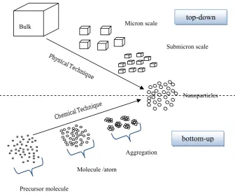
and bottom-up (see Figure 1.3).
Figure 1. 3. The two complementary approaches to nanoparticles synthesis. The top-down approach involves whittling down the size of materials from the bulk (macroscopic) to the nanometer scale. This approach generally relies on physical processes, or a combination of physical and/or chemical, electrical or thermal processes for their production. Usually the top-down approach is cost-effective but the control over the produced material is poor.
The bottom-up approach, on the contrary, involves assembling atom-by-atom, or molecule-by molecule into structures on the nanometer scale with properties varying according to the number of constituent entities/grain size. Building the system atom by atom or molecule by molecule guarantees the best control over all particles in the system. Colloidal dispersions such as
Micron scale
Submicron scale
Nanoparticles
Precursor molecule
Molecule /atom Bulk
Aggregation
top-down
microemulsions are a good example of the bottom-up concept of nanoparticles synthesis.
Both the top-down and the bottom-up approaches have been employed in this thesis for the synthesis of Cu2O nanoparticles (Chapter 2), to fabricate nanostructured Cu2O powders (Chapter 3), for the synthesis of CuO nanorod-like structures (Chapter 4) and to finally produce cuprite-based photonics inks (Chapter 5).
REFERENCES
1 B A Gizhevskii, Y. P. Sukhorukov, N. N. Loshkareva, A. S. Moskvin, E. V. Zenkov and E. A. Kozlov, “Optical absorption spectra of nanocrystalline cupric oxide: possible effects of nanoscopic phase separation”, J. Phys.:
Condens. Matter 17, 499–506, (2005) (http://arxiv.org/abs/cond-mat/0312009v1)
2 A. Mittiga, E. Salza, F. Sarto, M. Tucci, and R. Vasanthi. “Heterojunction solar cell with 2% efficiency based on a Cu2O substrate”. Applied Physics
Letters, 88, 163502, (2006).
3 D. Zhang, Y. Tang-Hong, Chun-Hua Chen, “Cu nanoparticles derived from CuO electrodes in lithium cells”, Nanotechnology, 16, 2338–2341, (2005). 4 J. B Goodenough, “Bond-length fluctuations in the copper oxide
superconductors,” Topical Review J. Phys.: Condens. Matter, 15, R257–R326, (2003).
5 R.V. Kumar, Y. Diamant, A. Gedanken, “Sonochemical synthesis of cerium oxide nanoparticles effect of additives and quantum size effect”, Chem.
Mater., 12, 2301, (2000).
6 S.T. Shishiyanu,T S. Shishiyanu and O. I. Lupa, “Novel NO2 gas sensor based on cuprous oxide thin films”, Sensors and Actuators B: Chemical, 113,[1],468-476,(2006)
7 J. Herion, E.A. Niekisch and G. Scharl, “Investigation of metal oxide/cuprous oxide heterojunction solar cells”, Solar Energy Materials, vol. 4, [1], 101-112, (1980).
8 G. Rothenberger, J. Moser, M. Gratzel, N. Serpone, and D. K. Sharma, “Charge carrier trapping and recombination dynamics in small semiconductor particles,” J. Am. Chem. Soc.; 107[26], 8054–8059,(1985).
9 S. Saito, M. Maryayama, K. Kaumoto, H. Yanagida, “Gas Sensing Characteristics of Porous ZnO and Pt/ZnO Ceramics”, J. Am. Ceram. Soc., 68, 40-43, (1985).
Pocaznoi, “Cuprous oxide films prepared by a low cost chemical deposition and photon annealing technique for sensors applications”, Proceedings of the
Third International Conference on Microelectronics and Computer Science, 1,
288–292,(2002).
11 E. Traversa, “Intelligent ceramic materials for chemical sensors,” J. Intel.
Mater. Syst. Struct., 6, 860, (1995).
12 R. Restori, D. Schwarzenbach, “Charge density in cuprite, Cu2O”, Acta
Crystallogr.B, 42, 201, (1986).
13 K. Borgohain, N. Murase, S. Mahamuni, “Synthesis and properties of Cu2O quantum particles”, Journal of applied physics, 92, [3], 1292–1297, (2002) 14 F. Biccari, “Defects and Doping in Cu2O”, PhD thesis, Università di Roma
Sapienza, (2009).
15 B. J. Wood, H. Wise and R. S. Yolles, “Selectivity and stoichiometry of copper oxide in propylene oxidation”, J. Catal., 15, 355, (1969).
16 E. Y. Wang, D. Trivich, H. Sawalha and G. Thomas, “Proc. COMPILES Int. Conf., Dhahran, Saudi Arabia, in Heliotech and Dev., 1, 643,(1976).
17 L. C. Olsen, F. W. Addis, and W. Miller. “Experimental and theoretical studies of Cu2O solar cells,” Solar Cells, 7, 247, (1982).
18 A. Mittiga, E. Salza, F. Sarto, M. Tucci, and R. Vasanthi, “Heterojunction solar cell with 2% efficiency based on a Cu2O substrate”, Applied Physics
Letters, 88, 163502, (2006).
19 M. Wei, N. Lun, X. Ma and S. Wen, “A simple solvothermal reduction route to copper and cuprous oxide”, Materials Letters, Vol. 61, [11-12], 2147-2150, (2007).
20 Musa A.O, Akomolafe T, Carter M.J., “Production of cuprous oxide a solar cell material, by thermal oxidation and study of its physical and electrical properties,” Solar Energy Mater Solar Cells, 51, 305–316, (1998).
Mater., 13, 952, (2001).
22 R.V. Kumar, Y. Mastai, Y. Diamant, A. Gedanken, “Sonochemical synthesis of amorphous Cu and nanocrystalline Cu2O embedded in a polyaniline matrix”, J. Mater. Chem., 11, 1209, (2001).
23 L. Armelao, D. Barreca, M. Bertapelle, G. Bottaro, C. Sada, E. Tondello, “A sol-gel approach to nanophasic copper oxide thin films”, Thin Solid Films, 442, 48–52, (2003).
24 S. Ghosh, D.K Avasthi, P. Shah, V. Ganesan, A. Gupta, D. Saransgi, R. Bhattacharya, W. Assmann, “Deposition of thin films of different oxides by RF reactive sputtering and their characterization”. Vacuum, 57,377–385, (2000).
25 P.R. Markworth, X. Liu, J.Y. Dai, W. Fan, T.J. Marks, R.P.H. Chang, “Coherent island formation of Cu2O films grown by chemical vapour deposition on MgO(110)”, J. Mater. Res., 16, 2408, (2001).
26 V.W. Klemm and W. Schuth, “Magnetochemical investigations: Magnetic measurements of cupric compound, a contribution to the theory of magnetism of transition elements”, Z. Anorg. Allg. Chem., 203, 104, (1931).
27 S. A. Sbrink and L.-J. Norrby, “A refinement of the crystal structure of copper(II) oxide with a discussion of some exceptional e.s.d.’s,” Acta
Crystallogr. B, 26, 8, (1970).
28 J. Bednorz and K. Muller, “Perovskite-type oxides-The new approach to high-Tc superconductivity”, Rev. Mod. Phys., 60, 585, (1988).
29 T. Kimura, Y. Sekio, H. Nakamura, T. Siegrist, and A. P. Ramirez, “Cupric oxide as an induced-multiferroic with high-Tc”, Nature Mater., 7, 291 (2008). 30 M. O’Keeffe and F. S. Stone, “The Magnetic Susceptibility of Cupric Oxide”,
J. Phys. Chem. Solids, 23, 161, (1962).
31 C-L Huang, E. Matijevic´, “Coating of uniform inorganic particles with polymers: III. Polypyrrole on different metal oxides,” Journal of Materials
32 K. Borgohain, J. B. Singh, M. V. Rama Rao, T. Shripathi, S. Mahamuni, “Quantum size effects in CuO nanoparticles”, Phys. Rev. B, 61, 11093- 11096 (2000).
33 Q. Wei, W. D. Luo, B. Liao, G.Wang, “Giant capacitance effect and physical model of nano crystalline CuO–BaTiO3 semiconductor as a CO2 gas sensor”,
J. Appl. Phys., 88, 4818, (2000).
34 L. Armelao, D. Barreca, M. Bertapelle, G. Bottaro, C. Sadac and E. Tondello, “A sol–gel approach to nanophasic copper oxide thin films,” Thin Solid Films, Vol. 442, [1-2], 48-52, (2003).
35 A. Catana, J-P. Locquet, S M. Paik and I.K. Schuller, “Local epitaxial growth of CuO films on MgO”, Phys. Rev. B, 46, 15477-15483, (1992).
36 D. Hana, H. Yang, C. Zhu and F. Wang, “Controlled synthesis of CuO nanoparticles using TritonX-100-based water-in-oil reverse micelles,” Powder
Technology, 185, [3], 286-290, (2008).
37 P Samarasekara, N T R N Kumara and N U S Yapa, “Sputtered copper oxide (CuO) thin films for gas sensor devices”, J. Phys.: Condens. Matter, 18, 2417–2420, (2006).
38 W. Wang, O.K Varghese, C. Ruan, M. Paulose and C. A Grimes, “Synthesis of CuO and Cu2O Crystalline Nanowires Using Cu(OH)2 Nanowire Templates”, J. Mater. Res., 18[12], 2756, (2003).
39 K. Borgohain and S. Mahamuni, “Formation of single-phase CuO quantum particles”, J. Mater., Res., 17, 1219-1223, DOI: 10.1557/JMR.2002.0180, (2002).
40 H. Gleiter, “Nanocrystalline Materials”, Progress in Materials Science, 33,223–315, (1989).
41 N. Ichinose, Y. Ozaki, and S. Kashu. “Superfine Particle Technology”,
Springer-Verlag, New York, (1988).
42 J. C. Maxwell, “A Treatise on Electricity and Magnetism,” 2nd ed., Oxford
University Press, Cambridge, (1904).
A. Siginer and H. P. Wang. Vol. 231/MD-Vol. 66. New York: The ASME, (1995).
44 J. A. Eastman, S. Choi, S. Li, W. Yu, and L. J. Thompson. “Anomalously Increased Effective Thermal Conductivities of Ethylene Glycol-Based Nanofluids Containing Copper Nanoparticles”, Applied Physics Letters, 78[6], 718-720, (2001).
45 A. Johnson, in: “New Materials by Mechanical Alloying Techniques”, (E. Arzt and L. Schults, eds.), Informationsgesellschaft Verlag, Calw-Hirsau, 354, (1988).
46 D. Chakravorty, and A. K. Giri. “Chemistry of Advanced Materials”. Ed. Rao, C. N. R. Boca Raton, FL: Blackwell Scientific Publication, (1993).
47 A.P. Alivisatos, “Semiconductor Clusters, Nanocrystals and Quantum Dots”,
Science, 271, 933, (1996).
2. Synthesis, characterisation, and stability of
Cu
2O nanoparticles produced via reverse
micelles microemulsion
1ABSTRACT
Cuprite (Cu2O) nanoparticles were synthesized at room temperature via reduction of CuCl2·2H2O by NaBH4 in water/n-heptane microemulsion stabilised by the nonionic Brij-30 surfactant. Whole Powder Pattern Modelling of the X-ray diffraction patterns shows the presence of a bimodal size distribution in the nanopowders, with a fraction of domains in the 10 - 40 nm range and a smaller one below 10 nm. Linear and planar defects are absent.
A relationship between the average size of the larger particles and the quantity of water in the system was obtained. The stability of cuprite under visible light irradiation both during the synthesis and after the preparation was investigated, showing that a self-catalytic conversion of Cu2O into CuO takes place in water.
2.1. INTRODUCTION
Nanoparticles of metals, semiconductors and oxides keep attracting the attention of the scientific community because of their exceptional and in some cases, unexpected physical and chemical properties coming from the quantum
1Part of the results shown in the present chapter have been published in: D. Dodoo-Arhin,
M. Leoni, P. Scardi, E. Garnier, A. Mittiga, “Synthesis, Characterization and stability of Cu2O nanoparticles produced via reverse micelles microemulsion”, Mater.chem. phys.,
doi:10.1016/j.matchemphys.2010.03.053 (on line).
confinement at the nano scale.
Synthesis of inorganic nanoparticles still remains a challenging task owing to intrinsic difficulties in the control of composition and morphology [1-3]. Among the proposed synthesis routes, water-in-oil (W/O) microemulsions are promising as they provide nanoreactors where size and morphology of nanoparticles can be well controlled [4-8].
Copper oxides are useful reference systems for the study of complex cuprates, most of which show high-Tc superconductivity. Of particular interest is cuprous oxide (Cu2O cuprite), a p-type semiconductor due to the presence of Cu vacancies which form an acceptor level 0.4 eV above the valence band [9].
As such, Cu2O is attracting the current interest owing to the wide range of potential applications. For instance, cuprite is a promising solar cell material (band gap of 2.0 - 2.2 eV [10]), but it can also be used as anode material for lithium ion batteries [11], as a photocatalyst for water splitting under visible light irradiation
[12, 13] and as a sensing material in gas detectors [9].
For a wider application of the material, however, it would be necessary to have powders characterised by a nanometric size and free of lattice defects, often required to maximise the efficiency of the corresponding devices. Unfortunately, it is not easy to obtain nanopowders of controlled size and shape, with an intermediate valence (Cu+ vs. Cu0 or Cu2+) and free of defects. Cu
2O particles with a controlled shape (e.g. cuboids [14], octahedral [15], or thick-shell hollow spheres
again a large quantity of defects seems always being present [19].
Furthermore, the analysis of the size of those nanoparticles as well as their structure is, in some cases, quite naive and can lead to severe errors (see e.g. [20]
for the description of a common mistake): most authors use simplified diffraction-based techniques (e.g. the Scherrer formula [21]) or Transmission Electron Microscopy for the size analysis. Quoting an average "crystallite size" or obtaining a size distribution from the analysis of a few dozen well visible grains has a limited statistical validity. Simple yet advanced techniques nowadays exists for a complete structural and microstructural characterisation of nanocrystalline powders, based on the analysis of the whole X-ray diffraction (XRD) pattern, either by using the Whole Powder Pattern Modelling (WPPM) technique [22], or by the Debye equation [23]. In WPPM, microstructural parameters such as domain size, shape and distribution, as well as type and quantity of linear and planar defects, are employed to build a computer-generated diffraction pattern of the material under study. The parameters are then varied through a nonlinear least squares routine until the best fit is reached between model and experimental data. This guarantees a self consistent extraction of microstructural information from the measured XRD pattern [22, 24].
In this part of the work we report some results on room-temperature synthesis and characterisation of Cu2O nanoparticles free of lattice defects. Powders produced via water-in-oil microemulsion and analysed both from the morphological, structural, microstructural and optical point of view, show a clear photoactivity.
2.2. EXPERIMENTAL
2.2.1. Materials and specimens
Two sets of five batches (40 ml each) of microemulsion were prepared (identified as SA and SB, plus the batch number). The two batches differ in the quantity of water (see below and cf. Table 2.1), i.e. in the parameter ω = nH2O/nBrij30, defined as the ratio between the number of molecules of water and surfactant in the system.
Sample Brij30® n-Heptane 0.2M CuCl2 NaBH4 H2O ω <D>
g
equiv.
ml g
equiv.
ml ml mg
% nm
SA1 6.287 6.62 22.430 32.99 0.4 31.0 1.0 1.3 16.8 SA2 6.289 6.62 22.158 32.99 0.8 61.0 2.0 2.6 12.1 SA3 6.285 6.62 21.891 32.99 1.2 92.0 3.0 3.8 10.0 SA4 6.286 6.62 21.613 32.99 1.6 122.0 4.0 5.1 15.0 SA5 6.287 6.62 21.345 32.99 2.0 152.0 5.0 6.4 16.1
SB1 6.284 6.62 22.434 32.99 0.4 31.0 1.0 1.3 29.7 SB2 6.286 6.62 22.153 32.99 0.8 61.0 2.0 2.6 14.5 SB3 6.286 6.62 21.886 32.99 1.2 91.0 3.0 3.8 10.0 SB4 6.284 6.62 21.614 32.99 1.6 122.0 4.0 5.1 15.0 SB5 6.286 6.62 21.332 32.99 2.0 152.0 5.0 6.4 16.1
Table 2. 1.Experimental parameters for the SA and SB sets. Both Brij30 and n-heptane have been weighted: the corresponding volume is reported for reference and to allow an easier calculation of ω.
hydrocarbon) after each mixing phase of the synthesis. The dispersion was sonicated for 3 min to favour the mixing of the two phases. Sonication was always done in a thermostatic bath (25 °C) at a frequency of 59 kHz and 125 W.
A 0.2 M solution of CuCl2.2H2O (Sigma Aldrich, 6174-250GF) was formed by adding the salt to deionised water (<1.8 μS/cm). Variable aliquots of this solution (1 to 5 vol%, according to Table 2.1) were added to the dispersion and sonicated for 6 min in order to create a homogeneous microemulsion. At the end of the process a homogeneous and transparent sky-blue microemulsion free from any precipitate was obtained.
Sodium borohydride (Sigma Aldrich, 99% purity, 213462-25G) was used as reducing agent: a 1 wt% (0.400 mg) was added to the emulsion and sonicated for 1s to start the reaction. To limit unwanted products (e.g. CuO), the microemulsion was continuously stirred for 10 mins. The addition of the reducing agent turned the emulsion first to yellow and then to deep brown, with evident evolution of gas and absence of any precipitation.
To break the microemulsion, 20 ml of Acetone (purity 99%, Sigma Aldrich) were added. Breaking the micelles causes the nanoparticles to slowly precipitate, with a powder clearly becoming visible on the bottom of the bottle after 10 min. To remove the organic phase residuals, 40 ml of a 1:1 mixture of Acetone and Ethanol (purity 98%, Sigma Aldrich) was added to the gelatinous precipitate, mildly sonicated and centrifuged at 6000 rpm for 10 mins. Subsequently 20 ml ethanol and 20 ml deionised water were added to the dispersion that was sonicated and centrifuged again at 6000 rpm for 10 mins.
The particles were further washed several times with deionised water. When needed for the analysis, the particles were laid on an h00 silicon wafer and dried under Argon flux.
°C and 9.5 mbar for 40 min to remove any residual Cu.
2.2.2. Characterisation techniques
X-ray powder diffraction (XRD) patterns were collected on a Rigaku PMG-VH Bragg-Brentano diffractometer operating a copper tube at 40 kV and 30 mA. The goniometer is equipped with a high resolution set up (1° divergence slit, 2° incident and diffracted beam Soller slits, 0.15 mm receiving slit) and a curved-crystal graphite analyser, providing a narrow and symmetrical instrumental profile over the investigated angular range.
The instrumental resolution function was characterised with the NIST SRM 660a (LaB6) standard [25]: all peak profiles were simultaneously fitted with symmetrical pseudo-Voigt functions whose width and shape were constrained according to the Caglioti et al. formulae [26]. The XRD patterns of all specimens were recorded in the 25°-85° 2θ range with a step size of 0.05° and a counting time of 60 s per step.
Microstructural analysis was performed using the Whole Powder Pattern Modelling (WPPM) method [22], using the PM2K software [27].
A Jeol JSM 5500 LV microscope operated at 20 kV was employed for the morphological characterisation: prior to investigation, specimens were sputtered with Au/Pd.
2.3. RESULUTS AND DISCUSSION
2.3.1 Synthesis
The redox potential for the Cu2+/Cu+ couple (Cu2+(aq)+ e-(aq) → Cu+(aq)) is +0.153 V, i.e. less than half of the +0.34 V needed to fully reduce Cu2+ to Cu0[28]. The water pools in reverse micellar solutions provide a large number of reaction sites which are separated from each other by the non-aqueous medium (oil/heptane) [29]. In aqueous solution, CuCl2 dissociates into [Cu(H2O)6]2+ ions (responsible of the sky blue colouring) and Cl- anions, that can partially coordinate with the copper ions. In [Cu(H2O)6]2+, the six water molecules completely surround the Cu2+ ion, shielding it. The addition of NaBH
4 to the microemulsion causes the following reaction (occurring in the water pools):
NaBH (s) 2H O4 + 2
⎯⎯
→
NaBO (aq)+ 4H (g)2 2 +heat (0.1)Hydrogen, interacting with the hydroxyl ions, causes the production of solvated electrons:
-
-H (g) 2O-H2 + →2H O 2 (aq)2 + e (0.2)
that can penetrate the hexaaquacopper(II) ion reducing it to Cu+(H
2O)x (x=1-4) ions. The accessibility of the copper ion in those complexes is highly favoured, as the coordination with water is less strong [30]. The reduced Cu+ ion can lead to the formation of cuprite via the following reaction chain (see e.g. [31]):
+ +
Cu (aq)+H O2 →CuOH(aq)+H (aq) (0.3)
2CuOH(aq)
⎯⎯
→
Cu O(s) H O2 + 2 (0.4)temperature, CuO can also form through the following scheme [31]:
+
-Cu (aq)+2OH (aq)→Cu(OH) (aq)2 (0.5)
2-Cu(OH) (aq) 2OH (aq)2 + − →Cu(OH) (aq)4 ←⎯→CuO(s) 2OH (aq) H O+ − + 2 (0.6)
The disproportionation of Cu+ can also lead to the full reduction of the copper ions to metallic copper as:
+ 2+ 0
2Cu (aq)→Cu (aq)+Cu (aq) (0.7)
Nanoparticles formed inside reverse micelles may undergo further growth or aggregation yielding particles larger than their initial nanodroplets, which may result in a bimodal size distribution.
2.3.2. X-ray diffraction analysis and transmission electron microscopy
30 40 50 60 70 80 0 10000 20000 30000 40000 22 2 31 1 22 0 21 1 20 0 11 1 SA5 SA4 SA3 SA2 Inte nsi ty(a.u)
2θ (degrees)
SA1
110
Figure 2 1.Diffraction pattern of the SA set of specimens. For better clarity, the remaining data are not shown.
The broadening of the line profiles decreases with the increase of ω this may indicate an increase in the size of the particles, as defects contribution to line profiles is expected to be negligible in a slow bottom-up synthesis such as the one investigated here. Quantitative microstructural information was obtained from XRD data by means of the recently developed WPPM approach [22], a physically-sound alternative to traditional Line Profile Analysis based on the Scherrer formula, Williamson-Hall or Warren-Averbach methods [21, 32, 33]. WPPM directly connects a physical model for the microstructure with the diffraction pattern, allowing an extraction of microstructure parameters without recurring to arbitrary peak shapes to fit diffraction peak profiles.
analysis leads to the conclusions that: (i) there is no evidence of additional contributions due to line defects, and in general no contributions to line broadening other than those from the small size of the crystalline domains; (ii) mean domain sizes range between a few nanometres (SA1) to nearly 20 nm (SA3) (see Figure 2.2), although standard deviations change quite significantly. Apparently, there is no evident correlation between mean domain size and ω when we assume a single mode distribution.
Sample (A) One Phase (B) Two Phases
ω <D>
nm
σ
nm
GoF k a0
Å <D> nm ω nm a0 Å <D> nm σ nm GoF
SA1 1.3 2.6 2.9 1.22 0.459 4.2644 17.6 8.6 4.2961 1.2 0.69 1.25
SA2 2.6 15 7.8 1.71 0.667 4.2623 25.6 11.4 4.2867 1.4 1.28 1.18
SA3 3.8 19 8.8 1.56 0.748 4.2637 34.4 5.9 4.2815 1.5 1.56 1.43
SA4 5.1 4.8 4.6 1.21 0.384 4.2602 37.5 11.7 4.2691 1.5 1.81 1.10
SA5 6.4 4.8 4.5 1.22 0.358 4.2589 41.9 4.2 4.2685 1.6 1.91 1.17
Table 2 2. Results of WPPM on the SA set of specimens. Data are reported with significant figures only. The column report the water/surfactant ratio ω, mean domain size <D> (calculated as first moment of the size distribution), variance of the distribution σ, cell parameter a0, scale parameter k and Goodness of Fit (GoF).
1 2 3 4 5 6 7 0 5 10 15 20 25
M
ean dom
ain size (
n
m
)
ω
Figure 2.2 Trend of the mean domain size (first moment of the lognormal
distribution) versus ω.
30 35 40 45 50 55 60 65 70 75 80
2 distributions
2θ (degrees)
1 distribution 0 5 10 15 20 25 in te n s it y ( x 1 0
3 cou
n
ts
)
is proposed both for the case of 2 distributions and 1 distribution. Residuals are drawn with a x3 magnification factor to highlight differences.
WPPM was thus tested by including a second independent domain size distribution (see Table 2.2), considering a different unit cell parameter (as if in a second cuprite phase) to account for possible surface relaxation effects frequently observed in nanocrystalline powders [34, 35]. It is worth underlining that, in the general case, the WPPM approach considers peak intensities as free parameters. Hence, to reduce parameter correlations and to allow for a more robust modelling, relative intensities were constrained to be the same in the two fractional components, and a scale parameter (k) was refined to determine the volume fractions of the two fractional components.
Although micellar systems are usually thought to provide a single and narrow distribution of domains [36, 37], bimodal distributions (sharp XRD peaks and quite broad tails) have been observed theoretically [38] and experimentally
[39]. From this point of view, the use of a method such as WPPM, which considers fine features of the diffraction pattern, is important: Scherrer formula or Williamson-Hall method, so far extensively used by the scientific community and based on the estimation of the sole line-profile breadth, easily miss the presence of small domains, related to features hidden in the tails of the diffraction peaks.
As shown by the Goodness of Fit (GoF) in Table 2.2, the quality of the modelling improves significantly when adding a second phase. As an example,
Figure 2.2 shows a comparison of the residuals for SA3 obtained by using single
and bimodal distributions in WPPM: the improvement when using two phases is quite evident. Figure 2.4(a) shows the size distributions for specimen SA1, SA3 and SA5. Distributions are multiplied by crystallite volume, so that the area under each distribution is directly equal to the volume fraction.
however, it is possible that a multimodal distribution is obtained, but the minority fraction is not taken into account or not thoroughly studied. For instance, a bimodal distribution has been observed in the micellar production of silver nanodisks by Maillard et al.[42]: the presence of large domains with a definite shape (discoidal in this case) plus a fraction of spherical nanometric domains is clear in the cited literature.
0 10 20 30 40 50 60
0.0 0.1 0.2 0.3 0.4 0.5 0.6 0.7 0.8
fr
action (a.u.)
D (nm)
SA1 SA3 SA5
0 1 2 3 4 5 6 7 0
5 10 15 20 25 30 35 40 45 50
SA1
SA2
SA3
SA4
SA5
SA1 SA2 SA3 SA4 SA5
D
iameter
(nm)
ω
XRD large domains XRD small domains simulation(b)
Figure 2. 4.(a) Bimodal particle size distribution for three representative specimens: SA1 (square), SA3 (circle) and SA5 (dot). In (b) the trends of average diameter versus ω. Diffraction data (larger domains, square; smaller domains, circle) are shown with results
of the simulation (as of Eq. (3), diamond).
A multimodal size distribution is evident, whose features are very similar to those observed in the cited paper [42]. The particles in the powder show also a wide size distribution: the SEM micrograph proposed as an example in Figure 2.6, shows a high degree of aggregation and the simultaneous presence of large and small particles in the system, particles that are large than the expected micelle size (a few nm).
Figure 2. 6. SEM micrograph of sample SA3 showing the presence of both large and small particles.
can be transferred and support the growth of the existing particle (autocatalysis). The larger the particle, the larger the area available for further growth. On the other hand, collisions between filled micelles can lead to growth of the larger particle due to phenomena such as Ostwald ripening, that would again favour larger particles with respect to smaller ones [41, 43]. The incidence of those phenomena is related to the rate of micelle encounter and to the rigidity of the surfactant protective layer. The more rigid the layer, the lower the exchange rate and, consequently, the lower the particle growth. Conversely, a less rigid layer would allow the micelles to be easily deformed: the exchange can then occur in completely filled micelles, allowing growth above the micelle size limit.
Ultrasonication employed to evenly distribute the reducing agent in the micelles may be responsible for the presence of the small particles: the excess energy introduced in the system by ultrasonication may promote an initial formation of an excess of nuclei that remained till the point of emulsion breaking
[44]. The absence of ultrasonication, on the other hand, would not allow a uniform nucleation in the system, whereas an excess ultrasonication may aid in weakening the surfactant film rigidity, thus promoting an excessive growth.
It is to exclude that growth occurred after the microemulsion was broken: breaking the surface tension using acetone just allows for precipitation of the particles under the influence of gravity. The surfactant is still protecting the surfaces at this stage: the subsequent removal of the organic phase using ethanol and water, also removes the possible reactants remained in the system, thus effectively limiting the possibility of further growth [45]. At this stage we would expect to see the formation of the nanoparticles aggregates observed under the TEM, more than the coalescence of existing domains.
The fraction of large crystal versus ω is shown in Table 2.2: SA3 has a larger fraction of large crystals (74.8%) with respect to the other samples. Figure
the average size of the larger fraction clearly increases with increasing ω. An increase in the water content reduces the interaction between the surfactant headgroups in the micelles and further weakens the surfactant layer rigidity. This shifts the nucleation mechanism from intramicellar to intermicellar, with a tendency to lower the nucleation rate, which favours an overall growth of larger particles [46].
Just for completeness, we report that the unit cell parameter of the two distributions is slightly decreasing with ω (cf. Table 2.2): this decrease is compatible with a surface relaxation effect, albeit a certain degree of correlation between cell parameter and specimen displacement (due to the non ideal specimen mount in the powder diffractometer) exists.
2.3.3 Modelling of the microemulsion system
In order to understand the correlation between the observed domain size (both in terms of sizes and appearance of a bimodal distribution), a deeper understanding of the micellar system and the modelling of its features are necessary.
2.3.3.1 Surfactant and Colloidal Science
Surfactants are low to moderate molecular weight compounds which modify the physico-chemical properties surfaces or interfaces of the media in which they are contained. Because of these features, they are referred to as Surface-active agents.
oil but readily soluble in water. Figure 2.7 shows a schematic representation of a surfactant molecule.
Due to the coexistence of polarities (polar head and non polar tail) in the molecule, surfactants are also referred to as amphiphilic compounds or amphiphiles. The amphiphilic nature of surfactants makes it possible to stabilize an immiscible water-oil mixture by reducing the interfacial tension between the two phases.
Figure 2. 7:Schematic representation of a surfactant molecule.
Short hydrocarbon (hydrophobic) chain surfactants are soluble in water while long chain surfactants are insoluble. The ability of surfactants to modify the physico-chemical properties of emulsions or colloidal dispersions make them very important in industrial applications such as asphalt emulsions, the paper industry laundering, industrial hard surface cleaning, inhibitor of corrosion, enhanced of oil recovery, personal care (cosmetics) products and coal transport [47, 48]. Owing to their varied applications, it is important to identify the specific type and/or class of surfactant for a specific application.
Surfactants can be classified based on their physical properties or functionalities. Accordingly, the following are some classification based on the nature of charge present on the hydrophilic group:
• Ionic (anionic and cationic) surfactant: Their solubilisation in water involves the ionization of the polar head. The charged polar head reacts with
ions in the solution. Sub-groups of this class are: anionic, which exhibits a negative charge, like as alkylbenzenesulfonate (RC6H4SO3-Na+), cationic, which bears positive charge, for example a salts of a long-chain amine, like as quaternary ammonium chloride (RN(CH3)3+Cl-) and zwitterionic (or
amphoteric), which carries a combination of the anion and cation characters.
Examples are the derivatives of phospholipids or amino-acids as sulfobetaine (RN-(CH
3)2CH2CH2SO3-). Their charge and property depend on the pH of the system which determines the dominating character of the molecule: anion with basic pH, cation with acid pH, and at their isoelectric point. They usually carry the two functions simultaneously.
• Nonionic Surfactants: They contain non-charged polar groups of which the affinity for water is due to the strong dipole-dipole interactions resulting from the hydrogen bonds. The function of this class of surfactant is modulated by the number of EO units which comprises the hydrophilic (polar) head and the length of its hydrophobic (hydrocarbon) tail. Brij30® (Polyoxyethylene 4 Lauryl Ether-(C2H4O)nC12H26O, nº4) is an example of this class: the structure of Brij30® is shown in Figure 2.8.
Figure 2. 8.Structure of the nonionic Brij 30 surfactant.
O
4
Head group OH
Research interest has been heightened in the use of non-ionic surfactants for reverse micelles for nanoparticles growth applications especially due to the unfavourable interactions between ionic reactants and surfactant groups.
Among the many unique properties that nonionic surfactants have over those of ionic surfactants with comparable hydrophobic groups:
• low critical micelle concentrations [49,

![Table 1. 1. Physical properties of Cu2O (partly from [14]).](https://thumb-us.123doks.com/thumbv2/123dok_us/814380.2076793/28.595.104.484.258.583/table-physical-properties-cu-o-partly.webp)


![Figure 2. 15. Mechanisms of nanoparticle formation in reverse micelles viaintermicellar exchange [67]](https://thumb-us.123doks.com/thumbv2/123dok_us/814380.2076793/80.595.121.472.347.656/figure-mechanisms-nanoparticle-formation-reverse-micelles-viaintermicellar-exchange.webp)

