BIBECHANA
A Multidisciplinary Journal of Science, Technology and Mathematics ISSN 2091-0762 (Print), 2382-5340 (0nline)
Journal homepage:http://nepjol.info/index.php/BIBECHANA
Publisher: Research Council of Science and Technology, Biratnagar, Nepal
Prunus domestica dye extraction for fabrication of zinc oxide based
dye-sensitized solar cells
Leela Pradhan Joshi
Department of Physics, Amrit Campus, Tribhuvan University, Kathmandu, Nepal E-mail:leela.pradhan@gmail.com
Article history: Received 19 August, 2015; Accepted 09 September, 2015 DOI:http://dx.doi.org/10.3126/bibechana.v13i0.13341
Abstract
Aluminium doped Zinc Oxide (AZO) seed layers were deposited on Fluorine doped Tin Oxide (FTO)
substrates using a spin coating technique. These were then immersed in growth solutions of zinc nitrate,
hexamethylenetetramine and distilled water to develop nanoplates of Zinc Oxide (ZnO). The
nanostructures of ZnO grown on FTO were studied using X-ray diffraction techniques. Dye-sensitized
solar cells (DSSC) were fabricated using two prepared electrodes, one of dye-loaded zinc oxide and
another that was platinum coated. The electrolyte used was potassium iodide iodine solution. The
performance of the assembled DSCCs was tested by drawing an IV curve. The results showed that the
short circuit current and open circuit voltages were about 10 microamperes and 270 millivolts
respectively.
©RCOST: All rights reserved.
Keywords: Zinc Oxide; Seed layers; Spin coating; Hydrothermal; Solar cells.
1. Introduction
In recent years a wide band semiconducting material ZnO has been an attractive and efficient material to
be utilized in fabrication of dye-sensitized solar cells [1-5]. ZnO can be prepared using several methods,
spin coating [6], spray pyrolysis [7], chemical bath deposition [8], dip coating [9]. Its morphology,
electronic as well as optical properties depend on method of preparation. ZnO is a very versatile material
because it's electrical and optical properties can be tailored by doping with different elements such as
Aluminium, Boron, Fluorine [10-12]. The fabrication of DSSC with various types of ZnO nanostructures
such as nanowires, nanoflowers, nanoribbons has been reported [1]. Another vital component which
affects the performance of DSSC is the type of dye extraction used to sensitize high band ZnO. Because
flowers can be used to fabricate solar cells [13-14]. This work reports the measurement on performance of
DSSC fabricated with nanoplates of ZnO and prunus domestica dye extraction.
2. Experimental
ZnO nanostructured films were grown by using a two-step spin coating and hydrothermal process on
glass as well as FTO substrates. A precursor solution was made using zinc acetate, diethanolamine, and
ethanol solution for spin coating [6]. Before coating the solution substrates were ultrasonically cleaned
using acetone and rinsed with distilled water several times. The growth solutions were prepared by
mixing equal molar concentrations of zinc nitrate and hexamethylenetetramine in distilled water at room
temperature. The AZO coated substrates were dipped into the growth solution at the constant temperature
of 905oC for 2 hours for the ZnO nanostructures to grow [15]. After taking out from the solution these
were rinsed with distilled water and dried in air at 4005oC for 30 minutes. Investigation on effect of
thickness of seed layer on optical property of ZnO has also been made in this work. Dye extraction from
the bark of prunus domestica is used to sensitize the ZnO layer. To extract the dye from prunus domestica
locally called as plums, we first collected few pieces of bark of prunus domestica. It is then cleaned and
dried in air. A 50gm of this is then dropped into ethanol and heated at constant temperature of 60±5oC for
2 hours which gives the nice red color solution. As-prepared ZnO films were characterized by using x-ray
diffraction, and ultra-violet visible spectrophotometer. We have measured the short circuit current and
open circuit voltage of assembled DSSC using Digital Fluke Multimeters. The absorbance spectrum of
dye extraction is measured using spectrophotometer. Above developed ZnO films were then dipped into
the dye solution at constant temperature of 60±5oC for 6 hours for dye loading. Finally, we assembled the
dye loaded ZnO electrodes and platinum coated counter electrode prepared by spin coating method using
5mM potassium iodide iodine liquid electrolyte solution [16]. The I-V curve of assembled DSSCs was
measured using two digital Fluke Multimeters Model 179.
3. Results and Discussion 3.1 Structural Properties
Figure 1 shows the X-ray diffraction pattern of ZnO film deposited on FTO substrate. The peaks
observed at 2θ= 35.38o(d = 2.53Ǻ), 37.84o(d= 2.37Ǻ) and 48.65o(d=1.86Ǻ) corresponds to ZnO peaks
orientating along (002), (101) and (102) planes respectively when comparison was made with standard
spectrum of Joint Committee on Power Diffraction Standards (JCPDS) values from PDF card # 361451
[6]. The XRD pattern also shows other low intensity ZnO peaks at 2θ = 56.14 o, 63.19o, 64.38oand 67.17owhich corresponds to (110), (103), (200), and (112) planes respectively. The d spacing values were
found to be slightly shifted from standard values which may be due to either Al doping in zinc acetate
solution or stress produced in the film. The FTO peaks were also significantly observed in the diffraction
Scherrer's formula, D= 0.9 λ/β cosθ [6-7]. The symbol λ, β, and θ represent the wavelength of X-ray ( 1.54Å), width of peak, and bragg's angle respectively. The average value of crystallite size was calculated
by measuring the full width half maximum (FWHM) of first two ZnO peaks of (002) and (101)
orientations and it was found to be of 239Å.
Fig. 1: X-ray diffraction pattern of ZnO film grown on FTO substrate at 90±5oC (Sample A5).
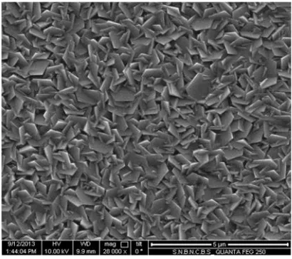
3.2 Scanning Electron Microscope
The previous report on study of morphology of the ZnO film prepared on glass substrate from 0.3M Al
doped zinc acetate precursor solution and 25mM growth solution is shown in Figure 2 below. It shows the
formation of nano-plate like structures. The average thickness and breadth of ZnO plates are of 96nm and
480nm respectively [17].
3.3 Optical Properties
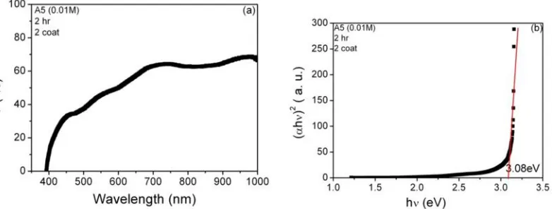
The optical transmittance curves as a function of wavelength for hydrothermally grown ZnO films on
FTO substrates at 90±5oC were shown in figure 3a (sample A1) and 4a (sampleA5) respectively. The
transmittances (T %) of all films were about 60% in the visible region. The band gap values were
estimated by the Manifacier method for the deposited ZnO films [6-10].To calculate band gap of ZnO the
graphs of ( h )2versus photon energy hn (eV) for films A1 and A5 were plotted where a represents the
absorption coefficient of ZnO. These graphs were shown in figure 3b and 4b respectively. By
extrapolating the linear portion of energy curves on hν axis gives the band gap of ZnO. The calculated
values of band gap of A1 and A5 are found to be 3.04eV to 3.08eV respectively. It is inferred that no
significant change in transmittance ( T%) as well as band gap on increasing AZO thickness from 1 coat to
2 coats while depositing ZnO films on FTO substrate in hydrothermal process.
Fig. 3: (a) Transmittance versus wavelength (b) (αhν)2 versus hν of ZnO film grown on FTO substrate
(Sample A1).
In this paper we have used the prunus domestica dye extraction to assemble DSSC. The captured
absorption spectrum of dye extraction is shown in figure 5a. The spectrum shows the absorption peak at
365nm. The ZnO nanostructured films dipped into the dye solution for 6 hours at 60oC for sufficient
amount to be adsorbed. Finally, the solar cell is assembled using as prepared ZnO photoanode, platinum
coated counter electrode of FTO and potassium iodide iodine redox electrolyte [16]. The performance of
encapsulated DSSC is tested by measurement of current voltage characteristic curve shown in figure 5b. It
clearly shows the same behavior of I-V curves for two different light intensities. Black colored filled
squares symbol in the figure represent the power generation from assembled dye-sensitized solar cell with
and 500W halogen light source and red filled circles represent the dark light of room only respectively.
The result showed the maximum short circuit current of about 10 microampere and open circuit voltage of
270 millivolts respectively.
Fig.5: (a) The absorption spectrum of prunus dye extraction solution.(b) Current voltage characteristic
curve of fabricated dye sensitized solar cell.
4. Conclusions
ZnO films were successfully deposited on glass and FTO substrates using an economic two step spin
coating followed by hydrothermal method. X-ray diffraction analysis confirms that the ZnO deposited
was of polycrystalline wurtzite structure. The average crystallite size of ZnO was 239Ǻ. An Optical
analysis showed that band gap of ZnO film was only slightly increased from 3.04eV to 3.08eV as the
thickness of seed layer was increased from 1 coat to 2 coats. The measurement on current voltage curve
of assembled ZnO based solar cell using prunus domestica dye extraction shows the short circuit current
References
[1] J. B. Baxter, and E. S. Aydil, Solar Energy Materials & Solar Cells, 90 (2006) 607. [2] M. Grätzel, Journal of Photochemistry and Photobiology, 4 (2003) 145.
[3] M. Krunks, T. Dedova, and I. O. Acik, Thin Solid Films, 515 (2006) 1157.
[4] S. -H. Lee, S. -H. Han, H. S. Jung, H. Shin, J. Lee, J.-H Noh, S. Lee, I. -S. Cho, J.–K. Lee, J. Kim, and H. Shin, Journal of Physical Chemistry C, 114 (2010) 7185.
[5] B. O’Regan, and M. Grätzel, Nature, 335 (1991) 737.
[6] S. P. Shrestha, S. R. Ghimire, J. J. Nakarmi, Y.-S. Kim, S. Shrestha, C.-Y. Park, and J.-H. Boo, Bull Korean Chemistry Society, 31 (2010) 1.
[7] U.Alver, T. Kılınç, E. Bacaksız, T. Küçükömeroģlu, S. Nezir, I. H. Mutlu, and F. Aslan, Thin Solid Films, 515 (2007) 3448.
[8] B. Cao, and W. Cai, Journal of Physical Chemistry C, 112(2008) 680.
[9] D. Djouadi, A. Chelouche, A. Aksas, and M. Sebais, Physics Procedia, 2 (2009) 701. [10] B. Joseph, P. K. Manoj, and V. K. Vaidyan, Ceramics International, 32 (2006) 487.
[11] B. N. Pawar, S. R. Jadkar, and M. G. Takwale, Journal of Physics and Chemistry of Solids, 66 (2005) 1779. [12] S. Tirado- Guerra, M. de la L. Olvera, A. Maldonado, and L. Castañeda, Solar Energy Materials & Solar
Cells, 90 (2006) 2346.
[13] B. Pradhan, S. K. Batabyal, and A. J. Pal, Solar Energy Materials and Solar Cells, 91(2007) 769. [14] N. M. Gómez-Ortíz, I. A. Vázquez-Maldonado, A. R. Pérez-Espadas, G.J. Mena-Rejón, J. A.
Azamar-Barrios, and G. Oskam, Solar Energy Materials & Solar Cells, 94 (2010) 40. [15] N. J. Nicholas, G. V. Franks, and W. A. Ducker, CrystEngComm, 14 (2012) 1232.
[16] S. S. Kanmani, K. Ramachandran, and S. Umapathy, International Journal of Photoenergy, 2012, Article ID 267824 (2012) 1.