Reference Vector Generation Technique to
Mitigate Voltage Sag with DVR
Ashwini Deshpande1, K.V.Ramamohan2
P.G. Student, Department of Electrical Engineering, MSSCET Engineering College, Jalna, Maharashtra, India1
Associate Professor, Department of Electrical Engineering, MSSCET Engineering College, Jalna, Maharashtra, India2
ABSTRACT: Voltage sag is one of the most important problem so the power quality which affects the new sensitive equipments. Voltage sags are short duration reductions in rms voltage caused by short circuits, overloads and starting of heavy motors, also the tripping of high-power adjustable-speed drives is probably the main voltage disturbance problem. So Voltage sag is much more of a global problem. Therefore detection methods are needed. For analysing the effects of voltage sag on these equipments, we need to establish a method for the voltage sags characterization. There are different detection methods for voltage sags such as RMS voltage detection, Fourier transform methods, missing voltage technique, novel detection. This research paper introduces voltage disturbance detection technique using reference vector generation with DVR on MATLAB software. Dynamic voltage restorer with reference vector Generation RVG is a effective method use to solve major power quality problem i.e. voltage sag. In this research, dynamic voltage restorer model is used to eliminate power quality problems. It works effectively and reduces the sag and minimise the harmonic which come from voltage source converter through the method reference vector generation (RVG)
KEYWORDS: power quality, voltage disturbance, RVG, MATLAB.
I. INTRODUCTION
Voltage sags are related to power quality problems .Voltage sags are short duration reductions in rms voltage caused by short circuits, overloads and starting of large motors. Voltage sag is much more of a global problem. Therefore for proper analysis and mitigation of voltage sag, their characterization is important. Existing methods for sag characterization are inadequate. There are many procedures for characterization of sags but they provide limited information that is insufficient for investigation of impacts on equipment.
In recent 10-15 years, with the rapid development of high and new technology, more and more power electronic devices based on computer and microprocessor control are used in power system. They are more sensitive to system interference than mechanical and electric equipment, so the higher attention to be pay for power quality disturbance .voltage sags are the most serious power-quality problems, as they are frequent causes of malfunctioning electrical equipments of end users [4].
.
Fig (1): Diagram of voltage sag [6]
In existing power-quality IEC Standard 60050, 1999 & IEEE Standard 1346, 1998 a voltage sag is defined as a short duration reduction of voltage magnitude in any or all of the phase voltages of a single-phase or a poly phase power supply at a point in the electrical system.
II. LITERATURE SURVEY
H. Kim exploited various operation modes and boundaries such as inductive operation, capacitive operation, and minimal power operation. The power flow of a voltage sag is analysed both in Minimal Energy Control method and In-Phase Control method. The operation of the Minimal Energy Control method is compared with that of the In-In-Phase Control method.
J. Nielsen, F. Blaabjerg and N. Mohan state different control strategies for dynamic voltage restorer are analyzed with emphasis put on the compensation of voltage sags with phase jump. Voltage sags accompanied by a phase jump are in some cases more likely to trip loads and satisfactory voltage compensation is more difficult to achieve. Different control methods to compensate voltage sags with phase jump are proposed and compared. Two promising control methods are tested with simulations carried out in Sober and finally tested on a 10 KVA rated Dynamic Voltage Restorer in the laboratory. Both methods can be used to reduce load voltage disturbances caused by voltage sags with phase jump. A generalized voltage restoration method is proposed by B. H. Li, S. S. Choi, and D. M. Vilathgamuwa. It can satisfactorily alleviate the phase angle jump and voltage wave form discontinuity associated with the energy-saving voltage restoration method used in the DVR. The method takes into account the characteristics of the voltage sag magnitude and phase-shift that may appear at the load bus as well as the voltage amplitude injection capability of the injection transformer
The solution to the power quality can be done from customer side or from utility side. First approach is called load conditioning, which ensures that the equipment is less sensitive to power disturbances, allowing the operation even under significant voltage distortion. The other solution is to install line conditioning systems that suppress or counteracts the power system disturbances. A flexible and versatile solution to voltage quality problems is offered by active power filters. Currently they are based on PWM converters.
III. RELATED WORK
The solution to the power quality can be done from customer side or from utility side. First approach is called load conditioning, which ensures that the equipment is less sensitive to power disturbances, allowing the operation even under significant voltage distortion. The other solution is to install line conditioning systems that suppress or counteracts the power system disturbances. A flexible and versatile solution to voltage quality problems is offered by active power filters. Currently they are based on PWM converters.
Some of the effective and economic measures can be as follows: 1. Thyristor Based Static Switches
2. Active Power Filters (APF)
3. Distribution STATIC Synchronous compensators (DSTATCOM) 4. DVR
Dynamic Voltage Restorer
Fig (2): Location of DVR
DVR, Dynamic Voltage Restorer is a distribution voltage DC-to-AC solid-state switching converter that injects three single phase AC output voltages in series with the distribution feeder and in synchronicity with the voltages of the distribution system. By injecting voltages of controllable amplitude, phase angle, and frequency (harmonic) into the distribution feeder in instantaneous real time via a series-injection transformer, the DVR can restore the quality of voltage at its load side terminals when the quality of the source side terminal voltage is distorted due to sensitive loads.
Discrete PWM-Based Control Scheme
In order to mitigate the simulated voltage sags in the test system of each compensation technique, also to compensate voltage sags in practical application, a discrete PWM-based control scheme is implemented, with reference to DVR. The aim of the control scheme is to maintain a constant voltage magnitude at the sensitive load point, under the system disturbance. The control system only measures the RMS voltage at load point, for example, no reactive power measurement is required. Figure (2) shows the DVR controller scheme implemented in MATLAB/SIMULINK. The DVR control system exerts a voltage angle control as follows an error signal is obtained by comparing the reference voltage with the RMS voltage measured at the load point. The PI controller processes the error signal and generates the
required angle δ to drive the error to zero, for example; the load RMS voltage is brought back to the reference voltage.
It should be noted that, an assumption of balanced network and operating conditions are made. The modulating angle δ
or delta is applied to the PWM generators in phase A, whereas the angles for phase B and C are shifted by 240° or -120° and 120° respectively.
VA= Sin (ωt +δ)
VB=Sin (ωt+δ-2π/3)
VC= Sin (ωt +δ+2π/3)
IV. REFERENCE VECTOR GENERATION DVR
The High sensitivity of electronic devices, employed for various applications such as computing, control, and power conversion, has made “quality power” an inevitable requirement. Voltage sag is one of the power quality problems that cause serious economic loss due to failure of equipment. Since it can occur even due to a remote fault in a system, it is more often than an interruption and can occur 20–30 times per year with an average cost of about $50 000 each in an industry. Voltage sag is a decrease in voltage (rms) between 0.1 and 0.9 per unit (p.u.) at power frequency.
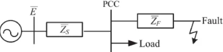
A model of voltage sag at the point of common coupling (PCC) is illustrated in Fig.(3) Typically, every sag is accompanied with phase jump. The phase jump occurs due to the difference in X/R ratio of the source (ZS) and feeder (ZF) impedances. Studies on effects of sags and the associated phase jumps at various point-on-wave instants reinforce the need to mitigate sags with phase jump. It substantiates that the phase jump creates imbalance [6].
In voltages, leading to transient overshoots in currents and resulting in detrimental effects on sensitive This can be done by using the method called RVG (reference voltage generation). The schematic diagram is shown in the fig.(4)below.
Fig (4): reference voltage generation in the form of vector [5]
The injected voltage is the vector sum of two phase voltages, and it is implemented using two injection transformers per phase, as shown in Fig. The topology shares the power to be injected among two phases at any instant of time. It can compensate complete range of sag in phase-a when the other two phases are healthy. However, when there are sags in the other phases too, the compensation capability of the topology is compromised. Since line voltages can provide increased compensation range [6], a topology is proposed in this paper to overcome the limitations in the compensation capability of the inter phase ac–ac topology. The ac–ac choppers in the sag supporters are fed with line voltages. Also it retains the merit of the inter phase.
Fig (5): Reference vector generation topology
topology, by having a sag supporter with two choppers and isolation transformers in each phase [4]. The secondaries of the isolation transformers are connected such that they add the output voltages of the choppers and inject them. Deriving the injected voltage from two voltage sources facilitates the realization of the desired reference voltage with phase shift. In this scheme, compensation of fundamental quantities has been considered. In case of harmonics, fundamental components are extracted and compensated by the scheme. A pulse-width-modulated (PWM) ac chopper placed between lines a and b with two bidirectional switches is depicted in Fig. A bidirectional feature in an insulated-gate bipolar transistor (IGBT) is achieved with a diode bridge. The chopper operates in buck mode, and the switching signal (T1) required to produce the desired output voltage is given to the switch Sab A. The complementary switching pulse is given to switch Sab B to provide a continuous load current. A small passive LC filter (Lfab and Cfab) is added at the output side to filter the high-frequency component. A filter is also added at the input side to avoid propagation of noise [2]. The filtered output voltages from each chopper are then added and injected using isolation transformers. The line voltages vtab, vtbc, and vtca are fed to the sag supporters.
Controller design by RVG
The control system of the DVR includes the detection of the voltage sags, injected voltage reference vref generation and control of this injected vCf voltage. When the source voltage is at its normal level, the DVR should be offline. When the voltage sag is detected, the DVR must go online very quickly and inject the required voltage to maintain the critical load voltage with the required level.
A. Voltage sag detection method
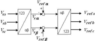
The proposed method for the detection of voltage sags is based on the alfa/beta vector magnitude vαβ which has a constant nominal value when no voltage sags occur. Therefore, it is only necessary to apply the Concordia transformation, and to calculate the alfa/beta vector magnitude to be able, by comparison with the nominal value, to detect symmetrical or asymmetrical voltage sags.
In the Concordia transformation, the subscripts a, b and c denote the source phase voltages. This method is complemented with a PLL to obtain constant amplitude sinusoidal alfa/beta reference voltages Vrefα, Vrefβ.
B. Voltage reference generation
The dc/ac converter should control the transformer voltages in order to compensate for any disturbance affecting the load voltage. The voltage reference signals for the sliding mode controller are obtained in the alfa/beta reference frame, as seen in Fig.
Fig (6) Principle of the voltage reference frame
V. EXPERIMENTAL RESULTS
To assess the performance of the proposed reference vector generation strategy, Digital simulation is done using the blocks of Matlab/simulink and the results are presented here.
The first simulation was done with no DVR and no three phase fault is applied to the system. This system shows the normal operating power system without DVR and three phase fault. Fig (a) shows the simulation results of normal operating system with no DVR.
Fig.(a): 3-Ø Voltage at Load Point, Without 3-Ø Fault, Without DVR
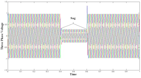
The second simulation is done in fig.(b) with no RVG and a three phase fault is applied to the system at point with fault resistance of 0.66 p.u for a time duration of 200 ms. Fig (b) shows the simulation results of 3-Ø fault, Without RVG.
Fig (b): 3-Ø Voltage at Load Point, With 3-Ø Fault, Without RVG
.
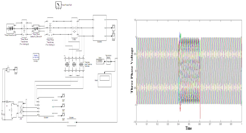
Fig.(c) Matlab model With RVG method Fig (d): 3-Ø Voltage at Load Point, with controlled 3-Ø Fault, with RVG
Reference voltage generation during the sag period is shown in following fig (d) & (e) respectively through the matlab simulation. When the DVR is in operation the voltage interruption is compensated almost completely and the RMS voltage at the sensitive load point is maintained at normal condition. Injected voltage and the voltage across load ..FFT analysis for the output voltage is shown in Fig.(d) THD reduces to 0.39%. Thus the harmonics are reduced from 1.37% to 0.39%.
Fig (d) Fig (e)
VI. CONCLUSION
An reference vector generation strategy is proposed in this paper, from the various research paper related to power quality problems, it has found that there are so many power quality issues like voltage sag, swell, spikes, transient and harmonic which is very harmful to power system.
method use to solve major power quality problem i.e. voltage sag. In this research, dynamic voltage restorer model is used to eliminate power quality problems. It works effectively and reduces the sag and minimizes the harmonic which come from voltage source converter through the method reference vector generation (RVG).
REFERENCES
[1] J. Nielsen, F. Blaabjerg and N. Mohan, Control Strategies for Dynamic Voltage Restorer. Compensating Voltage Sags with Phase Jump, Applied Power Electronics Conference and Exposition, ,Vol. 2, pp. 1267-1273,2001.
[2] H. Kim, “Minimal Energy Control for A Dynamic Voltage Restorer”, Power Conversion Conference, PCC Osaka, Vol. 2, pp. 428- 433, 2002 [3] D. Vilathgamuwa, A. RanjithPerera, and S. Choi, “Voltage Sag Compensation With Energy Optimized Dynamic Voltage Restorer”, IEEE
Transactions on Power Delivery, Vol. 18, No. 3, pp. 928-936, July 2003
[4] S. S. Choi, B. H. Li, and D. M. Vilathgamuwa, “Dynamic Voltage Restoration with Minimum Energy Injection”, IEEE Transactions on Power Systems, Vol. 15, No. 1, pp. 51-57, February 2000
[5] J. Nielsen, F. Blaabjerg and N. Mohan, “Control Strategies for Dynamic Voltage Restorer. Compensating Voltage Sags with Phase Jump”, Applied Power Electronics Conference and Exposition, Vol. 2, pp. 1267-1273, 2001.
[6] B. H. Li, S. S. Choi, and D. M. Vilathgamuwa, “A New Control Strategy For Energy-Saving Dynamic Voltage Restoration” Power Engineering Society Summer Meeting, Vol. 2, pp. 1103-1108, 2000.
ACKNOWLEDGMENT
It is privilege for me to have been associated with Prof. K.V. Ramamohan, Electrical Engineering Department, MSS’S college of engineering and technology, Jalna my guide, during this work. I am thankful to him, for his constant inspiration and valuable guidance, carefully reading and editing my work and always boosting my confidence to complete my work.
Also, I would like to thank respected HOD & all the staff members of the department of MSS’s collage of engineering and technology, Jalna for their continuous support.
I would be failing in my duties if I do not make a mention of my family members including my parents and my brothers for providing moral support, without which this work would not have been completed.
This kind of work cannot be finished without many others help, even some of them are aware of their contribution and importance in producing this paper. It is a great pleasure for me to take this opportunity to express my gratefulness to all of them.
BIOGRAPHY
Miss. Ashwini S Deshpande, was received Bachelor of Engineering degree in the stream Electrical Electronics & Power Engineering(EEP) from P.E.S. College of Engineering, Maharashtra, DR.BAMU University, Aurangabad and Pursuing Master degree in Electrical Power System (EPS) from the Matsyodari Shikashan Santha’s College of Engineering and Technology Jalna. Dr. BabaSaheb Ambedkar Marathwada University, Aurangabad.
Mr.K.V.Ramamohan, was received M.Tech Degree from SPRCET J.N.T. University, Hyderabad and B.Tech. Degree from SKTRMCE, J.N.T.University, Hyderabad. Presently he is working as an Asst.Professor in the Dept. of Electrical Engineering, from MSS’s Engineering College, Jalna, Maharashtra.
![Fig (1): Diagram of voltage sag [6]](https://thumb-us.123doks.com/thumbv2/123dok_us/1641743.1205166/1.595.193.414.639.737/fig-diagram-of-voltage-sag.webp)
![Fig (4): reference voltage generation in the form of vector [5]](https://thumb-us.123doks.com/thumbv2/123dok_us/1641743.1205166/4.595.193.404.541.735/fig-reference-voltage-generation-form-vector.webp)