ABSTRACT
XIAOPENG, WANG. Power Efficiency Conscious Design and Implementation of High Frequency Integrated Synchronous Buck DC-DC Converters for Portable Electronics Applications. (Under the direction of Dr. Alex. Q. Huang.)
This dissertation focuses on the efficiency analysis, efficiency conscious design, and silicon implementation of integrated synchronous Buck DC-DC converters (ISBC) with switching frequencies equal to or larger than 4MHz. Using switching frequencies in this range makes the ISBC compact enough to satisfy the component size specifications required by modern portable electronic devices such as smartphones, laptops, tablet computers, and personal satellite navigation systems.
subcells for a specified load current. The predicted results correctly explain the characteristics of efficiency improvement via segmentation.
The second part of the dissertation focuses on the implementation and its control algorithm used for automatic segmentation in a 4MHz ISBC. State-of-art automatic segmentation techniques use a current sensor to adjust the number of active power FET subcells, causing the obtained efficiency will deviate from the designed value because of MOSFET Rdson variations in a practical environment. The implementation of an on-chip current sensor is another challenge in >4MHz ISBCs. Moreover, decreasing the silicon area and current consumption of the high resolution A/D converter, the smooth transfer between pulse width modulation (PWM)/pulse frequency modulation (PFM), and the safe operation of the segmented power stage during load transients all are practical issues that are under-addressed by state-of-art designs. The dissertation proposes a Vsw pinning automatic segmentation technique (VswPS). VswPS maintains the time sampled value of Vsw (the phase node voltage of the ISBC) in a voltage band for all load conditions by turning on or off a given number of power FET subcells. It is concluded from the viewpoint of the algorithm that VswPS not only ensures optimal segmentation but also automatically accounts for Rdson variations. From the viewpoint of implementation, as there is no need for a current sensor or an A/D converter, the challenges of circuit design are significantly reduced, and the segmentation technique can be applied to a >4MHz ISBC. VswPS also efficiently supports the automatic mode shift between PWM and PFM. The silicon circuit schematic and layout of the ISBC with VswPS are introduced in the dissertation and the performance of the ISBC is verified by simulation.
Power Efficiency Conscious Design and Implementation of High Frequency Integrated Synchronous Buck DC-DC Converters for Portable Electronics Applications
by Xiaopeng Wang
A dissertation submitted to the Graduate Faculty of North Carolina State University
in partial fulfillment of the requirements for the Degree of
Doctor of Philosophy
Electrical Engineering Raleigh, North Carolina
2010
APPROVED BY:
________________ ________________
Dr. Paul D. Franzon Dr. W. Rhett Davis________________ ________________
DEDICATION
To my wife, Li Yang
my son, Chengzhi Wang
And my parents,
BIOGRAPHY
ACKNOWLEDGEMENTS
I wish first to thank my advisor, Dr. Alex. Q. Huang, who brought me into this research area and continuously supported me throughout my Ph.D study. His extensive knowledge, broad vision, creative thinking and consistent exploration of new technology inspire me to bravely face the challenges I encountered and actively look for a better solution during my entire study and research work. I would also like to express my gratitude to Dr. Paul Franzon, Dr. W. Rhett Davis, Dr. Srdjan Lukic, Dr. Nathan Reading and Dr. Xun Liu, for serving on my committee. I thoroughly enjoyed the classes taught by Dr. Paul Franzon and Dr. W. Rhett Davis. I also got much help from Dr. Srdjan Lukic, Dr. Nathan Reading and Dr. Xun Liu; their knowledge in different fields was a valuable resource for my research work. I also want to thank Prof. Ruoping Yao and Prof. Fangquan Rao at Shanghai JiaoTong University, Prof. Zhengzhi Wang and Prof. Junming Liu at the National University of defense technology, and Prof. Lin Gao at Nanjing University of Aeronautics and Astronautics. I sincerely appreciate their help and encouragement in the past years.
TABLE OF CONTENTS
LIST OF TABLES... xvi
LIST OF FIGURES ... xviii
Chapter 1. Introduction ……….. 1
1.1. Background ... 1
1.2. ISBC operation and power efficiency ... 4
1.2.1. CCM mode and PWM modulation ………... 4
1.2.2. DCM mode and PFM modulation in light load ... 7
1.2.3. Loss breakdown in high frequency ISBC …... 8
1.2.4. Power efficiency improvement techniques ... 13
1.2.4.1 Dynamic gate voltage .……… 13
1.2.4.2 Gate swing control ….……… 13
1.2.4.3 PFM modulation …….……….. 14
1.2.4.4 Power width modulation …….……… .. 14
1.2.4.5 Dithering skip modulation ……… 15
1.2.4.6 Dead-time adjustment ……… 15
1.3 Dissertation outline ……….. 17
References ... 19
2.1. Introduction ... 22
2.1.1 Present state of switching loss analysis ………. 24
2.1.1.1 Power FET parameters measurement ……… 25
2.1.1.2 Power FET time domain behavior based switching loss calculation ... 27
2.1.1.3 Assumptions violation ………... 29
2.1.1.4 Other comments ………... 33
2.1.2 What is expected in a novel switching loss analysis ……….. 33
2.2. Breakdown of switching loss ... 34
2.3. O_loss analysis ……….. 36
2.3.1 PFET turn-on event ……….………... 38
2.3.1.1 Miller plateau equations ……… 38
2.3.1.2 Miller plateau criterion………..……… 40
2.3.1.3 O_loss during PFET turn-on ……… 42
2.3.2. PFET turn-off event .………... 43
2.3.2.1 Miller plateau analysis ……… 44
2.3.2.2 Miller plateau criterion ……… 45
2.3.2.3 O_loss during PFET turning off ………... 47
2.3.2.4 Dead-time set dead t2_ setting ………... 48
2.3.3 NFET turn-on event ……….……….. 50
2.3.4 NFET turn-off event ……… 51
2.3.4.1 sign confliction ……… 52
2.3.4.2 Dead-time set dead t1_ setting ………. 52
2.4 C_loss classification ………. 54
2.4.2.1 Active power FET cells ………... 57
2.4.2.2 Inactive power FET cells ……….……… 63
2.4.2.3 C_loss summary ………. 69
2.5 Capacitor energy variation hypothesis and parasitic capacitance extraction ………. 70
2.5.1 Capacitor energy variation hypothesis ………. 70
2.5.2 Capacitance extraction ……… 72
2.5.2.1 Kdb ……….. 74
2.5.2.2 KGDO ……… 78
2.5.2.3 Kox ………... 82
2.5.3 Hypothesis verification ………. 84
2.5.3.1 Verification case 1 ………... 85
2.5.3.2 Verification case 2 ……….. 87
2.5.3.3 Verification case 3 ………. 89
2.5.3.4 Verification case 4 ………... 91
2.5.3.5 Verification case 5 ………... 93
2.5.3.6 Verification case 6 ………... 95
2.5.3.7 Verification case 7 ………... 97
2.5.3.8 Verification case 8 ………....99
2.5.3.9 Verification case 9 ………..101
2.5.3.10 Verification case 10 ………..103
2.5.3.11 Verification case 11……… 105
2.5.3.12 Verification case 12……… 107
2.6 Driver design and D_loss ……… 111
2.6.1 D_loss ……… 112
2.6.3 N_N selection ………... 117
2.7. Conclusions and future work ... 118
References ... 119
Chapter 3. Power stage design and optimization ………... 123
3.1. Power filter and PID control ... 123
3.1.1 System specification ………... 123
3.1.2 Output filter ………124
3.1.2.1 Power inductor ……… 124
3.1.2.2 Power capacitor ……… 125
3.1.2.3 Ripple and MPS value calculation ……… 125
3.1.3 PID controller ……… 127
3.1.3.1 Small signal transfer function ………127
3.1.3.2 PID compensator ……… 130
3.1.3.3 Transient response simulation ……… 133
3.2 Power FET optimal sizing ……….……….… 134
3.2.1 Switching loss ………. 134
3.2.1.1 O_loss ……… 134
3.2.1.2 C_loss ………. ……… 136
3.2.1.3 D_loss ……… 137
3.2.1.4 Total switching power loss ……… 138
3.2.2 Power FET conduction loss ………... 138
3.3 Load efficiency curve ……….. 141
3.3.1 Switching loss ………. 141
3.3.2. Power PFET Conduction loss ……… 142
3.3.3 Dead-time conduction loss ……… 142
3.3.4 Copper loss ……… 145
3.3.5 Circuit power loss ……… 145
3.3.6 Total power loss and efficiency ……… 146
3.4 Segmentation and power loss ………….………. 148
3.4.1 Switching loss ………. 148
3.4.2 Conduction loss ……….. 150
3.4.3 Total loss ……… 150
3.4.4 Load efficiency curves for ISBC with segmentation ………. 150
3.4.4.1 Incorrect W/N assumption ……….. 151
3.4.4.2 Load efficiency curves ………. ……… 151
3.4.5 Chip test …...…...……….………..………….………. 160
3.5. Conclusions and future work ... 162
References ... 163
Chapter 4. Silicon implementation of automatic segmentation .…….. 165
4.1. State-of-art techniques ………... 166
4.1.1 Load current information based segmentation ………. ... 166
4.1.2 Challenges ………….……… 169
4.1.2.1 Optimal segmentation ………..……… 169
4.1.2.3 Temperature variation and self-heating effect ……… 178
4.1.2.4 Circuit challenges ……… 180
4.1.2.5 Summary ………..……… 181
4.2. Vsw pinning segmentation ... 183
4.2.1 VswPS concept ………... 183
4.2.2 VswPS principle and parameter setting ……… 186
4.2.2.1 Vsw principle ………...……… 186
4.2.2.2 Segmentation resolution bits …….…………...……… 187
4.2.2.3 Permanently active subcells ………..188
4.2.2.4 VswPS convenient grouping ……… 189
4.2.2.5 Threshold voltage setting ………..… 190
4.2.2.6 VswPS typical operation ……….. 193
4.2.3 Rdson compensation ……… 195
4.3. VswPS solid state circuit ... 196
4.3.1 Segment sensor ……….……….. 198
4.3.1.1 Latched pipeline comparator ………...……… 199
4.3.1.2 Reliable operation block ………...……….. 206
4.3.1.3 Current consumption and silicon layout …….……… 208
4.3.2 PFM/PWM mode transfer ………. 209
4.3.2.1 PWM operation ………...……… 210
4.3.2.2 PFM operation ………..………...……….. 213
4.3.2.3 From PWM to PFM …….………...……… 218
4.3.2.4 From PFM to PWM …..………...……… 221
4.4.2 Segmentation & no PFM ….……….………. 225
4.4.3 PFM & No segmentation ….……….……. 226
4.4.4 Segmentation & PFM ………...………. 227
4.4.5 Efficiency comparison ………..………. 228
4.5. VswPS compensation verification ... 230
4.5.1 ISBC with VswPS in 0oC temperature ….………. 231
4.5.2 ISBC with VswPS in 200oC temperature ….………. 232
4.5.3 Comparison of CIS and VswPS ..……….……. 234
4.6. Conclusions and future work ………... 235
References ... 238
Chapter 5. Maximum switching frequency, choke effect and digital
pulse width modulator ... 241
5.1. Background ... 242
5.1.1. Digital DC-DC converter ... 242
5.1.2. Potential advantages ... 244
5.1.3. Issues for portable applications ... 245
5.2. DPWM resolution ... 246
5.2.1. Least resolution requirement ... 246
5.2.2. Hardware resolution ... 247
5.2.2.1. Counter hardware resolution ... 247
5.2.2.2. Delay_mux hardware resolution ... 249
5.2.3.1. Dither soft resolution ... 251
5.2.3.2. Sigma-delta soft resolution ……... 253
5.3. MSF in digital DC-DC converters ... 254
5.3.1. Top level architectures ... 254
5.3.2. MSF limitations ... 256
5.3.2.1. Top level timing constraint ... 257
5.3.2.2. Hardware implementation limitation ... 259
5.4. Fan-out-of 4 ... 259
5.5. MSF & DPWM architecture ... 260
5.5.1. Counter DPWM ... 260
5.5.1.1. Maximum clock frequency ... 261
5.5.1.2. MSF analysis ... 263
5.5.1.3. Frequency control ... 264
5.5.1.4. Revised version … ... 265
5.5.2. Delay_mux DPWM ... 265
5.5.2.1. Fastest delay chain ... 266
5.5.2.2. MSF analysis ... 267
5.5.2.3. Frequency control ... 268
5.5.2.4. Revised version ... 269
5.5.3. Self-oscillation hybrid DPWM ... 270
5.5.3.1. Restraint clock frequency ... 271
5.5.3.2. Choke effect and choke region ... 274
5.5.3.3. MSF analysis …... 277
5.5.3.6. Power dissipation ... 280
5.5.4. Non-self-oscillation hybrid DPWM ... 281
5.5.4.1. Digital programmable delay cells ... 282
5.5.4.1.1. One kind of delay cell ... 283
5.5.4.1.2. Another kind of delay cell ... 285
5.5.4.2. Maximum output frequency ... 287
5.5.4.3. MSF analysis ... 287
5.5.4.4. Relative matching error ...289
5.5.4.5. Frequency control ... 290
5.5.4.6. Power dissipation ... 290
5.6. Choke relaxed SOH DPWM ... 291
5.6.1. Choke relaxed SOH DPWM ... 291
5.6.2. Counter clock frequency ... 294
5.6.3. Maximum output frequency ... 295
5.6.4. Choke effect and choke region ... 296
5.6.5. MSF analysis ... 298
5.6.6. Relative matching error ... 299
5.6.7. Effective delay_mux hardware resolution ... 300
5.6.8. Frequency control ... 301
5.6.9. Power dissipation ... 301
5.7. Silicon implementation ... 302
5.7.1. Top level schematic and die micrograph ………... 303
5.7.2. Current starved delay cell ... 307
5.7.3. Synchronous counter ... 308
5.7.4. Phase locked loop ... 309
5.7.4.2. Charge pump ... 309
5.7.5. 64:1 multiplexer ... 310
5.8. Performance test ... 312
5.8.1. Test circuit and bench …………... 313
5.8.2. Maximum and minimum output frequency ... 317
5.8.3. Duty cycle input response ... 319
5.8.4. Linearity and monotonicity …………... 320
5.8.5. Power dissipation breakdown ... 324
5.8.6. Silicon area breakdown ... 325
5.9. Conclusions and future work ... 326
5.9.1. Architectures comparison ... 326
5.9.1.1. MSF comparison ... 326
5.9.1.2. Relative matching error comparison ... 327
5.9.1.3. Frequency control comparison ... 328
5.9.1.4. Power dissipation comparison ... 328
5.9.1.5. Silicon area comparison ... 328
5.9.2. Chip data collection ... 329
5.9.3. Future work ... 329
5.9.3.1. Wide range frequency control ... 329
5.9.3.2. DPWM soft resolution ... 330
5.9.3.3. Linearity improvement ... 330
5.9.3.4. Multi-phase implementation ... 330
5.9.3.5. Integration of dead time optimization ... 330
Chapter 6. Summary of contributions ………... 342
6.1. Event based switching losses analysis ... 342
6.2. Vsw pinning automatic segmentation ... 345
LIST OF TABLES
Table 2-1. ISBC unit width C_loss summary for active power FET subcells …………. 67
Table 2-2. ISBC unit width C_loss summary for inactive power FET subcells ………. 68
Table 2-3. Working condition of ISBC for parasitic capacitance extraction ………72
Table 2-4. Working conditions of ISBC for hypothesis verification ……….. 84
Table 2-5. First verification case of ISBC hypothesis ………. 85
Table 2-6. Second verification case of ISBC hypothesis ……… 87
Table 2-7. Third verification case of ISBC hypothesis ………89
Table 2-8. Forth verification case of ISBC hypothesis ………91
Table 2-9. Fifth verification case of ISBC hypothesis ………93
Table 2-10. Sixth verification case of ISBC hypothesis ……….. 95
Table 2-11. Seventh verification case of ISBC hypothesis ………. 97
Table 2-12. Eighth verification case of ISBC hypothesis ………...……… 99
Table 2-13. Ninth verification case of ISBC hypothesis ………100
Table 2-14. Tenth verification case of ISBC hypothesis ………103
Table 2-15. Eleventh verification case of ISBC hypothesis ……….. 105
Table 2-16. Twelfth verification case of ISBC hypothesis ……….107
Table 2-17. Hypothesis verification results summary ………109
Table 2-18. Parasitic component values extracted in BSIM3V3.1 level 49 model of AMI06 process (T=100oC, TT corner) ……….. 110
Table 2-19. Driver sizing symbols ………..……….. 111
Table 2-20. P_P impact on ISBC switching performance ………... 116
Table 2-21. Parameters relative to the selectedP_Pvalue ………117
Table 3-3. The truth table of the driver logic ……… 161 Table 4-1. MOSIS wafer acceptance tests report for V03M run [4-8] ……….. 175 Table 4-2. Major parameters relative to Rdson and capacitance in MOSIS BSIM3V3.1
LIST OF FIGURES
Figure 2-16. Miller plateau onset analysis in the power PFET turn-on transient …….... 38 Figure 2-17. Miller plateau onset analysis in the power PFET turn-off transient ………44 Figure 2-18. Miller plateau onset analysis in the power NFET turn-on transient……... 50 Figure 2-19. Miller plateau onset analysis in the power NFET turn-off transient ….…...52 Figure 2-20. Five typical loops accomplishing the capacitor charging and discharging ..55 Figure 2-21 First two sub-stages in PFET turn-on event ……….……….58 Figure 2-22 Third sub-stage in PFET turn-on event ………….……….. 59 Figure 2-23 C_loss classification in PFET turn-on event ………..……….. 59 Figure 2-24 Two sub-stages in PFET turn-off event and C_loss classification ……….. 60 Figure 2-25 Two sub-stages in NFET turn-on event and C_loss classification ……….. 61 Figure 2-26 Two sub-stages in NFET turn-off event and C_loss classification ………. 62 Figure 2-27 Inactive cells two sub-stages and C_loss classification when PFET turns on ……… 63 Figure 2-28 Inactive cells two sub-stages and C_loss classification when PFET turns off ……… 64 Figure 2-29 Inactive cells two sub-stages and C_loss classification when NFET turns on ……… 65 Figure 2-30 Inactive cells two sub-stages and C_loss classification when NFET turns off ……… 66 Figure 2-31. Capacitor energy variation in a switching transient ……… 71 Figure 2-32. The ISBC schematic for capacitance extraction ……… 73 Figure 2-33. Four switching events labeled in time sequence ………... 73 Figure 2-34. Kdb_P related unit energy in the working condition for extraction
(case 2 and 3) ………76 Figure 2-35. Kdb_N related unit energy in the working condition for extraction
(case1 and 4) ………77 Figure 2-37. Kdb_Nrelated unit energy in the working condition for extraction
(case1 and 4) ….……… 77 Figure 2-38. KGDO_Prelated unit energy in the working condition for extraction
(case2 and 3) …..……… 80 Figure 2-39. KGDO_Prelated unit energy in the working condition for extraction
(case1 and 4) ………80 Figure 2-40. KGDO_Nrelated unit energy in the working condition for extraction
(case2 and 3) ..……… 81 Figure 2-41. KGDO_Prelated unit energy in the working condition for extraction
(case1 and 4) ……….. 81 Figure 2-42. Kox_P related unit energy in the working condition for extraction (case3) 83 Figure 2-43. Kox_Nrelated unit energy in the working condition for extraction (case 4) 83 Figure 2-44. Kdb_P related unit energy in 1st working condition for hypothesis
verification ……… 85 Figure 2-45. Kdb_N related unit energy in 1st working condition for hypothesis
verification ………….……… 85 Figure 2-46. KGDO_P related unit energy in 1st working condition for hypothesis …. 86 Figure 2-47. KGDO_N related unit energy in 1st working condition for hypothesis …… 86 Figure 2-48. Kox related unit energy in 1st working condition for hypothesis
verification ………….……… 86 Figure 2-49. Kdb_P related unit energy in 2nd working condition for hypothesis
Figure 2-51. KGDO_P related unit energy in 2nd working condition for hypothesis
verification ……….. 88 Figure 2-52. KGDO_N related unit energy in 2nd working condition for hypothesis
verification ………...…… 88 Figure 2-53. Kox related unit energy in 2nd working condition for hypothesis verification ….……… 88 Figure 2-54. Kdb_P related unit energy in 3rd working condition for hypothesis
verification …….……… 89 Figure 2-55. Kdb_N related unit energy in 3rd working condition for hypothesis
verification…..……… 89 Figure 2-56. KGDO_P related unit energy in 3rd working condition for hypothesis
verification ………. 90 Figure 2-57. KGDO_N related unit energy in 3rd working condition for hypothesis
verification ………. 90 Figure 2-58. Kox related unit energy in 3rd working condition for hypothesis verification ….……… 90 Figure 2-59. Kdb_P related unit energy in 4th working condition for hypothesis
verification…..……… 91 Figure 2-60. Kdb_N related unit energy in 4th working condition for hypothesis
verification…..……… 91 Figure 2-61. KGDO_P related unit energy in 4th working condition for hypothesis
Verification.……… 92 Figure 2-62. KGDO_N related unit energy in 4th working condition for hypothesis
….……… 92 Figure 2-64. Kdb_P related unit energy in 5th working condition for hypothesis
verification.………..……… 93 Figure 2-65. Kdb_N related unit energy in 5th working condition for hypothesis
verification.……… 93 Figure 2-66. KGDO_P related unit energy in 5th working condition for hypothesis
verification ……….……… 94 Figure 2-67. KGDO_N related unit energy in 5th working condition for hypothesis
verification ………. 94 Figure 2-68. Kox related unit energy in 5th working condition for hypothesis verification ….……… 94 Figure 2-69. Kdb_P related unit energy in 6th working condition for hypothesis
verification………..……… 95 Figure 2-70. Kdb_N related unit energy in 6th working condition for hypothesis
verification………..……… 95 Figure 2-71. KGDO_P related unit energy in 6th working condition for hypothesis
verification.……….……… 96 Figure 2-72. KGDO_N related unit energy in 6th working condition for hypothesis
verification ………. 96 Figure 2-73. Kox related unit energy in 6th working condition for hypothesis verification ….……… 96 Figure 2-74. Kdb_P related unit energy in 7th working condition for hypothesis
Figure 2-76. KGDO_P related unit energy in 7th working condition for hypothesis
verification……..……… 98 Figure 2-77. KGDO_N related unit energy in 7th working condition for hypothesis
verification ………. 98 Figure 2-78. Kox related unit energy in 7th working condition for hypothesis verification ….……… 98 Figure 2-79. Kdb_P related unit energy in 8th working condition for hypothesis
verification……..……….… 99 Figure 2-80. Kdb_N related unit energy in 8th working condition for hypothesis
verification………...……….…99 Figure 2-81. KGDO_P related unit energy in 8th working condition for hypothesis
verification…………...………100 Figure 2-82. KGDO_N related unit energy in 8th working condition for hypothesis
verification ……….100 Figure 2-83. Kox related unit energy in 8th working condition for hypothesis verification ….………100 Figure 2-84. Kdb_P related unit energy in 9th working condition for hypothesis
verification………..………101 Figure 2-85. Kdb_N related unit energy in 9th working condition for hypothesis
verification………..…………101 Figure 2-86. KGDO_P related unit energy in 9th working condition for hypothesis
verification………..……… 102 Figure 2-87. KGDO_N related unit energy in 9th working condition for hypothesis
….………102 Figure 2-89. Kdb_P related unit energy in 10th working condition for hypothesis
verification………..………103 Figure 2-90. Kdb_N related unit energy in 10th working condition for hypothesis
verification………..………103 Figure 2-91. KGDO_P related unit energy in 10th working condition for hypothesis
verification ……….104 Figure 2-92.KGDO_N related unit energy in 10th working condition for hypothesis
verification ………. 104 Figure 2-93. Kox related unit energy in 10th working condition for hypothesis
verification…………...………104 Figure 2-94. Kdb_P related unit energy in 11th working condition for hypothesis
verification………...………105 Figure 2-95. Kdb_N related unit energy in 11th working condition for hypothesis
verification………..………105 Figure 2-96. KGDO_P related unit energy in 11th working condition for hypothesis
verification ……….106 Figure 2-97KGDO_N related unit energy in 11th working condition for hypothesis
verification ………. 106 Figure 2-98. Kox related unit energy in 11th working condition for hypothesis
verification………106 Figure 2-99. Kdb_P related unit energy in 12th working condition for hypothesis
Figure 2-101.KGDO_P unit energy in 12th working condition for hypothesis verification ….………108 Figure 2-102KGDO_N related unit energy in 12th working condition for hypothesis
verification ………...108 Figure 2-103. Kox related unit energy in 12th working condition for hypothesis
verification………108 Figure 2-104. The impact of P_P on z1 ……….. 113 Figure 2-105. The impact of P_P on P on
g
V _ ……… 113
Figure 2-106. The impact of P_P on PFET turn-off MPoff ………….………. 114 Figure 2-107. The impact of P_P on power loss ………. 114 Figure 2-108. Transient current pulse and switching delay when PFET turns on …… 115 Figure 2-109. Transient current pulse and switching delay when PFET turns off …… 116 Figure 3-1. 4MHz ISBC power stage for a portable application ………... 126 Figure 3-2 ISBC components for small signal modeling ……….. 127 Figure 3-3. Bode diagram of the ISBC power stage ……….. 130 Figure 3-4. Type-III PID compensator and parameters ……… 131 Figure 3-5. Bode diagram of loop gain transfer function …….………. 132 Figure 3-6. Transient response of the ISBC when load current step changes up and down ….………133 Figure 3-7. 3-dimension value of the power loss specified in (3-40) ……...…………..139 Figure 3-8. Zoomed-in version of Figure 3-7 ……… 140 Figure 3-9 Model prediction and simulation based load efficiency curves of
when the ISBC operates in the #1 working condition ………..….. 152 Figure 3-12. Incorrect W/N predicted load efficiency curves for seven kinds of
segmentation when the ISBC operates in the #1 working condition …….... 153 Figure 3-13. Simulation and prediction based load efficiency curves for three kinds of segmentation when the ISBC operates in the #1 working condition………. 154 Figure 3-14. Simulation measured load efficiency curves for seven kinds of segmentation when the ISBC operates in the #2 working condition ……….. 155 Figure 3-15. Predicted load efficiency curves for seven kinds of segmentation
when the ISBC operates in the #2 working condition ………..….. 156 Figure 3-16. Incorrect W/N predicted load efficiency curves for seven kinds of
segmentation when the ISBC operates in the #2 working condition …….... 156 Figure 3-17. Simulation and prediction based load efficiency curves for three kinds of segmentation when the ISBC operates in the #2 working condition………. 157 Figure 3-18. Simulation measured load efficiency curves for seven kinds of segmentation when the ISBC operates in the #3 working condition ……….. 158 Figure 3-19. Predicted load efficiency curves for seven kinds of segmentation
when the ISBC operates in the #3 working condition ………..….. 158 Figure 3-20. Incorrect W/N predicted load efficiency curves for seven kinds of
segmentation when the ISBC operates in the #3 working condition …….... 159 Figure 3-21. Simulation and prediction based load efficiency curves for three kinds of segmentation when the ISBC operates in the #3 working condition………. 159 Figure 3-22. ISBC using logic controlled driver to realize segmentation ………. 161 Figure 3-23. Silicon layout of the ISBC chip for loss analysis experimental
Figure 4-5. The shift of loss balance point due to Rdson variation ……….. 173 Figure 4-6. The shift of loss balance point due to parasitic capacitance variation …… 174 Figure 4-7. Deviation of parasitic capacitance relative parameters in AMI06 SCN05 technology’s different manufacturing runs ………..176 Figure 4-8. Deviation of Rdson relative parameters in AMI06 SCN05 technology’s different manufacturing runs ………176 Figure 4-9. PMOS Rdson with MOSIS BSIM3V3.1 level 49 Spice corner models …..178 Figure 4-10. PMOS Rdson variation due to Ids, Vds, corners and temperatures …….. 179 Figure 4-11. On chip sense-FET current sensor [4-14] ………..……….. 180 Figure 4-12. Concept of Vsw pinning automatic segmentation ………..……….. 183 Figure 4-13 State machine to support the VswPS technology ……….. 185 Figure 4-14. The ranges of load current for different number of active subcells
when the load current decreases ……… 192 Figure 4-15. The ranges of load current for different number of active subcells
Chapter 1
Introduction
The dissertation’s focus is the power efficiency analysis and improvement of the high frequency (in the range of several megahertz) integrated DC-DC synchronous Buck converters (ISBC), which are widely utilized as power supply modules for portable digital devices, such as global positioning system (GPS) receivers, laptop computers, personal digital assistants (PDA) and smart phones.
1.1 Background
Portable digital devices have many performance expectations to the ISBC [1-1] [1-2] [1-3] [1-4] [1-5] [1-6] and the most important four of them are respectively,
1) Power supply quality
An ISBC with the performance as close as an ideal voltage source is expected by advanced digital devices. In state-of-art electronics market, an example expectation for the ISBC is that the worst case voltage perturbation should be less than 50mV when the load current varies [1-5] in the full range.
2) Component size
devices. Increasing the switching frequency of ISBC to several megahertz is the solution adopted by recent commercial ISBC designs [1-26] [1-27] [1-28] [1-29] [1-30] [1-31] to minimize the size of these discrete components.
3) Wide range load current and dominant time for light load condition
More and more functional blocks are being integrated into portable devices so that the customers is able to use the portable devices for various kinds of activities, such as browsing websites, communication, watching movies, playing games and operating office software. The current demands of these functional blocks are significantly different, so the ISBC load current is supposed to vary in a wide range. At the same time, though how long each functional block will be in the work mode heavily depends on the customer’s personal interest, a popular fact is that during most of its operation time the portable devices will operate in light load (<0.1A) or deep light load condition (<0.01A).
4) Power conversion efficiency
Both switching frequency and load current influence ISBC power conversion efficiency.
Switching frequency is determined from the consideration of power supply quality and component size. In theory, the higher the switching frequency is, the higher the bandwidth of ISBC regulator can be designed to be and the smaller the power component is. However, parasitic components in MOSFET and its package impede the trend towards high switching frequency in the respect of power efficiency and switching noise.
ISBC in a wide range of load current. The power FET width of the ISBC is optimized at 1A load current. The efficiency will achieve a peak value of 91.51% at the optimized load condition but drop to 21.54% when the load current is 0.02A.
The above four important expectations of the ISBC conclude that the development trend of portable devices will require a high switching frequency ISBC and the efficiency of the ISBC is required to have high power conversion efficiency in a wide load range. An ideal solution is a constant efficiency value or a flat efficiency curve independent of load current. The desire towards the ideal solution motivates the research in the dissertation, which includes developing a switching loss analysis method so that it is possible to explain how well some nowadays technologies can improve the efficiency; proposing a better solution in both the temperature compensation and the silicon implementation; and modifying the state-of-art architecture of some component to doubly increase its capacity for high switching frequency implementation without sacrifice of power loss.
1.2 ISBC operation and power efficiency
1.2.1 CCM mode and PWM modulation
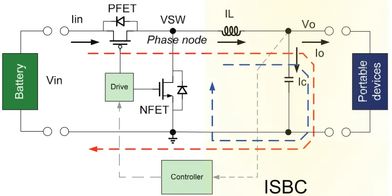
The output DC voltage level of the ISBC is tightly regulated with the aid of feedback control. The controller in Figure 1-2 compares the output voltage of ISBC with a reference voltage which represents the expected output voltage of the ISBC and utilizes control algorithm to generate a periodic square wave signal with adjustable pulse width at the input of the driver. This kind of output voltage regulation implementation is called pulse width modulation (PWM). The driver will sufficiently strengthen the driving capacity of the periodical square wave so that it is strong enough for turning on and off two big power MOSFETs. For the ISBC fabricated in standard CMOS technology, two power MOSFETs include a PFET as the control (top) power FET and a NFET as the synchronous (bottom) power FET.
Figure 1-3 illustrates the turn on sequence of the two power FETs and an ideal voltage waveform VSW at the phase node of the ISBC due to the switching. As illustrated in Figure 1-3, the two power FETs are alternately turned on so that in theory there is no direct shoot through route between the power source and the ground in the ISBC. Furthermore, on consideration of the existence of parasitic component, two dead-time
intervals set dead
t1_ and set dead
t2_ are artificially inserted in the time sequence of the driver signal
to avoid parasitic induced direct shoot through in a practical product.
When the control power FET and the synchronous FET are driven in the above alternating way, the ISBC is called to work in a continuous conduction mode (CCM). The simulation waveforms of the ISBC working in the CCM are illustrated in the subsection 4.3.2.
When the control FET turns on, the input voltage will appear at the phase node. As the input voltage is higher than the output voltage, the power inductor and capacitor will be charged and store energy. When the control FET turns off, the electrical connection between the battery and the load device is cut off and the output energy is maintained by the discharge of the power inductor and capacitor. If the synchronous FET is not immediately turned on after the control FET turning off because of the deadtime or vice versa, the synchronous FET’s body diode will help transfer the current discharged by the power inductor with a forward voltage drop as 0.6-0.7V. As the output voltage Vo is only around 1V in nowadays low power portable devices, the body diode conduction implies significant power loss. The body diode conduction will be eliminated when the deadtime passes and the synchronous FET is completely turned on.
1.2.2 DCM mode and PFM modulation in light load
In subsection 1.2.1, the CCM operation of ISBC is introduced. However, the ISBC does not always work in the CCM and sometimes it will prefer to work in a discontinuous conduction mode (DCM) so as to improve power conversion efficiency when the load current is very small (light or deep light load condition).
Because of the existence of the inductor current ripple, the valley value of inductor current in CCM might be negative when the load current is very small. The negative inductor current implies over-charging/discharging of the inductor and a deficient efficiency. DCM is generated with the aid of an inductor current sensor or directly comparing the phase node voltage VSW with the ground as VSW will change from a negative voltage to a positive one when the inductor current goes from positive to negative. When the inductor current zero crossing happens, the synchronous NFET will be turned off to terminate the further discharge of inductor current and the inductor current is maintained at zero until the next period of charging process begins. The ISBC in DCM is typical of the periodic inductor current waveform illustrated in the subsection 4.3.2. Also, the critical load current between CCM and DCM is usually selected as a value a little higher than half of the inductor current peak-to-peak ripple.
The avoidance of the over-charging/discharging of the inductor significantly benefits the power efficiency, as the switching frequency of the ISBC in DCM will be roughly linear proportional to the load current to ensure that the averaging inductor current equals the load current. The equation is derived in the subsection 4.3.2.
implementation is to develop two kinds of controller for the ISBC in wide range of load current. The first one is the PWM linear regulator introduced in subsection 1.2.1 for the normal load condition, and the second on is a pulse frequency modulation (PFM) nonlinear controller for the light load condition. In the PFM regulation, various kinds of output voltage ripple hysteresis controller [1-8] are applied and the switching frequency is modulated according to the load current. The PFM regulation method in this dissertation is constant on-time control in which the turn on time of the control FET is set to be a constant value [1-8]. It should be mentioned that PFM regulation is not a good choice for the normal or heavy load condition, as the switching frequency might become very high and finally lose control in the situation [1-8] [1-9] [1-10] [1-11] [1-12].
1.2.3 Loss breakdown in high frequency ISBC
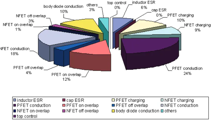
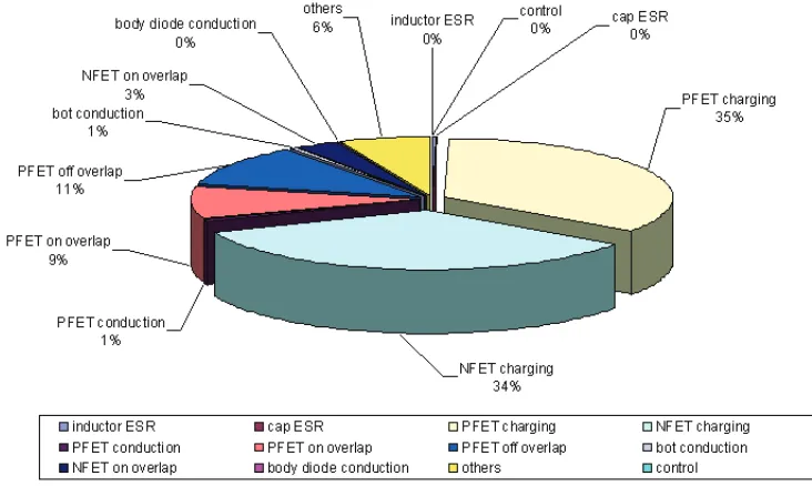
power MOSFET will generate charging/discharging loss and the Rdson of the power MOSFET in the linear region will generate conduction loss. Besides, as the power MOSFET is loaded by a power inductor, the power FET will temporally work in the saturation region during the switching transient. Thus, overlap loss as the times of Vds and Ids in the short period will exist in the ISBC.
Figure 1-4 illustrates the possible sources of power losses in the ISBC. PFETC refers to the conduction loss of the power FET which is generated by the rdson of the power MOSFET working in the linear region. PFETSW indicates the switching losses of the power FET including the charging/ discharging loss of its parasitic capacitance and the overlap loss generated during the swithcing. PFETDrv refers to the charging and discharging losses in the power FET driver. PIND is related to the direct current resistance (DCR) of the power inductor and PCAP indicates the losses generated by equivalent series resistance (ESR) of power capacitor. PBdC refers to the NFET body diode conduction loss during the dead-time and Prr accounts for body diode’s reverse recovery energy loss. Among the aforementioned losses, the conduction loss, the switching loss and the driver loss are dominant and directly related to the width of the power MOSFET. Furthermore, the switching losses and the driver loss are positively linear proportional to the power MOSFET width; while the conduction loss is inversely proportional to the width. Thus, there is a power loss tradeoff process when we determine the width of the power FET and the process is called power FET sizing. The optimal efficiency will be achieved when a power FET width makes the switching and driving loss exactly 50% to 50% balanced with the conduction loss. The power FET sizing is usually carried out at a normal load condition so that the power efficiency of the ISBC will be the highest when the load current equals its normal value
charging/discharging loss is independent of the load current. As a result, when ISBC works at a load current in different from the normal one, either the conduction loss or the switching and driver loss will be larger than the other and the efficiency drops down because of the broken balance. For example, when the load becomes heavier, the conduction loss will be dominant. On the contrary, when the load current is lighter, the switching and driver loss becomes dominant.
1.2.4 Power efficiency improvement techniques
There are many techniques to improve the efficiency of the ISBC working in a wide range of load current and the subsection will introduce several major circuit design related techniques.
1.2.4.1 Dynamic gate voltage
Increasing the gate voltage can decrease the rdson of the power MOSFET so as to decrease the conduction loss. However, the practice will at the same time increase the switching and driver loss. On the other hand, decreasing the gate voltage will increase the conduction loss but decrease the switching and driver loss. Thus, if the gate voltage were able to be dynamically adjusted with the load current, the balance between the switching and the conduction loss might be improved to some extent. Texas instruments applied the technique in a commercial product [1-13] and the reported maximum efficiency difference between two different gate voltages (VGS 9V and VGS 5V ) is 4% at 20A load current and 8% at 2A load current.
The dynamic gate voltage technique requires extra circuits for example charge pumps or DC/DC boost converters to supply multiple levels of driver vdd DC voltages higher than Vin.
1.2.4.2 Gate swing control
voltage does not swing between zero and driver vdd, while swing between some voltage level and driver vdd.
With the technique, 2% efficiency improvement was reported in the light load condition when the load current is 0.03A and 7% efficiency improvement was reported in the deep light load condition when the load current is 0.01A [1-14].
1.2.4.3 PFM modulation
PFM mode is an imperative choice when the ISBC works in a deep light load condition. However, PFM mode is not a good choice when the ISBC works in the normal load condition as discussed in subsection 1.2.2.
1.2.4.4 Power width segmentation
Power width segmentation technique means that the number of active power FET subcells in the ISBC is controllable and is regulated when the load current changes [1-15] [1-16] [1-17] [1-18] [1-19]. Figure 1-8 illustrate the layout of the ISBC power FET subcells with the segmentation technique. The power width segmentation technique can increase the power efficiency by 3%-8%. From the load efficiency curve reported in [1-15], the maximum efficiency improvement was 8% at the critical load current before the ISBC entered into PFM mode operation.
1.2.4.5 Dithering skip modulation
The dithering skip modulation [1-20] technique changes the modulation of the ISBC so that digital signal processing technique can be utilized to equivalently decrease the switching frequency in a sequence of many switching cycles so that power efficiency is improved. The technique had issues on the output voltage regulation and small signal modeling. There is still a long way to go for applying digital signal processing to control or modulate the ISBC - a high frequency real time system.
The reported maximum efficiency improvement [1-20] is 8%, when both the dithering skip modulation and the dead-time adjustment technique are adopted.
1.2.4.6 Dead-time adjustment
As introduced in subsection 1.2.1, the insertion of set dead
t1_ and set dead
t2_ between PFET and
NFET driver signal are imperative to avoid the parasitic induced shoot through in the ISBC. If the shoot through happens because of too small values of deadtime, efficiency will be hugely degraded and the safe operation of the ISBC is also in doubt. On the other hand, the existence of deadtime indicates that ISBC will have certain time of body diode
conduction and the larger deadtime implies larger period of body diode conduction. For low voltage ISBC applications such as portable applications, the body diode conduction degrades the efficiency significantly too. Thus, in order to obtain an optimal efficiency, we need to select the minimum values of set
dead
t1_ and set dead
t2_ which is large enough to avoid
the parasitic induced shoot through.
The issue is that the switching transient depends on the load current, so the minimal required values of set
dead
t1_ and set dead
t2_ are load current dependent too. The dependence will
be details analyzed in Chapter 2 and the conclusion there is that the required deadtime will be increased when the load current is decreased. Thus, if we select the values of
set dead
t1_ and set dead
t2_ to satisfy the minimum deadtime requirement in the light load condition,
in the heavy load condition the selected values are too conservative and a long period of body diode conduction will be generated.
On the basis of the discussion, if we can adjust the values of set dead
t1_ and set dead
t2_ in
different load condition, the load efficiency will be obviously improved. Many industrial practices verified the analysis [1-20] [1-21] [1-22] [1-23] [1-24].
The implementation of dead-time adjustment is easy in theory but severely difficult in practice. As the value of deadtime is usually several nanoseconds, if the deadtime is aggressively adjusted, the existence of uncertain factors including switching noise, temperature variation, technology corner and packaging might make the parasitic induced shoot through happen in the ISBC and hereby the damage of the ISBC chip.
1.3 Dissertation outline
Among those efficiency improvement approaches introduced in subsection 1.2, the power width segmentation and the PFM operation will be selected in the dissertation for a 4MHz ISBC for portable applications. The dissertation includes three research topics to improve the selected technologies. As there is no method available now to analyze how well the efficiency can be improved by power width segmentation technique, the first topic is to develop a general power efficiency analysis which can be used for the ISBC with the power width segmentation technique. The second topic is to overcome several implementation issues existing in the state-of-art automatic segmentation technique and effectively integrate the segmentation technique and the PFM technique in one chip. The dissertation also has a topic about the digital version of the ISBC, which will make efforts on how to improve the maximum switching frequency of a digital ISBC.
In the Chapter 2, an event based switching loss analysis method will be introduced. The method will physically separate the charging/discharging loss and the overlap loss. Two criteria for Miller plateau in PFET switching will be developed. A hypothesis about parasitic capacitor energy variation will be proposed and its verification will be implemented with 12 different fabrication processes, working conditions, or design corners. Charging/discharging losses for all switching events will be classified for each parasitic capacitor so that the losses can be calculated with the capacitor energy variation. Equations for dead-time setting and gate driver optimization will also be developed in the Chapter 2.
Chapter 4 will focus on the design and silicon implementation of automatic segmentation in an ISBC. With the developed switching loss analysis equations in Chapter 2, the optimal number of active power FET cells in a specified condition will be derived. The challenges of the state-of-art segmentation implementation will be discussed and a novel segmentation technique will be proposed to overcome the challenges. All power FET cells will be managed with state machine. Moreover, some specific techniques to ensure the safe operation of automatic segmentation during load transient and the smooth mode shift between PWM and PFM will be developed.
Chapter 5 will be involved in the analysis and design of a digital pulse width modulator (DPWM). The chapter discusses why DPWM determines the maximum switching frequency (MSF) of a digital ISBC. Fan-out-of-4 (FO4) metric will be utilized to predict the MSF of different state-of-art DPWM architectures in a specified semiconductor technology. Also, different approaches to improve the MSF will be discussed. Furthermore, the MSF limitation of self-oscillation hybrid DPWM architecture (SOH) will be investigated, which is the most popular architecture in current practice. A novel architecture will be proposed to doubly improve the MSF in SOH through architecture modification without sacrifice of silicon area and power.
References
[1-1] A. J. Stratakos, “High-Efficiency Low-voltage DC-DC Conversion for Portable Applications,” Ph.D dissertation, University of California, Berkeley, Elec. Eng. Dept., 2001.
[1-2] J. Xiao, “An Ultra-Low-Quiescent-Current Dual-Mode Digitally-Controlled Buck Converter IC for Cellular Applications,” Ph.D dissertation, University of California, Berkeley, Elec. Eng. Dept., 2003.
[1-3] J. Alvarez, “Power management for Portable Applications,” Texas Instruments, http://batterypoweronline.com/eprints/free/tisept05.pdf, 2009.
[1-4] M. Davidson, “Understanding Portable Applications Requirements to Improve System Performance,” National Semiconductor.
[1-5]. Intel document number: 306761-001, “Voltage Regulator Module (VRM) 10.2L Design Guidelines”, March 2005.
[1-6]. A. P. Chandrakasan and R. W. Brodersen, Low Power Digital CMOS Design. Kluwer Academic Publishers, 1995, Ch.5.
[1-7]. R. W. Erickson and D. Maksimovic, Fundamentals of Power Electronics. Kluwer Academic Publishers. 2001.
[1-8] J. Sun, “Characterization and performance comparison of ripple-based control for voltage regulator modules,” IEEE Trans. Power Electron. Vol.21, No.2, pp.346-353, Mar. 2006.
[1-9]. R. Miftakhutdinov, “An analytical comparison of alternative control techniques for powering next-generation microprocessors,” Texas Instrument seminar, 2002.
[1-10] Y. Y. Mai, and K. T. Mok, “A constant frequency output-ripple-voltage-based Buck converter without using large ESR capacitor,” IEEE Trans. Circuits and Systems-II. Vol.55, No.8, pp.748-752, Aug. 2008.
[1-12]. P. Li, L. Xue, P. Hazucha, T. Karnik, and R. Bashirullah, “A delay-locked loop synchronization scheme for high-frequency multiphase hysteretic DC-DC converters,”
IEEE Journal of Solid-State Circuits. Vol.44, No.11, pp. 3131-3145, July 2009.
[1-13]. S. Mappus, Texas application report, “Optimizing MOSFET characteristics by adjusting gate drive amplitude,” SLUA341, June, 2005.
[1-14]. M. D. Mulligan, B. Broach, and T. H. Lee, “A constant-frequency method for improving light-load efficiency in synchronous Buck converters,” IEEE power electronics letters, vol. 3, No. 1, pp. 24-29, March, 2005.
[1-15]. O. Trescases, G. Wei, A. Prodic, and W. T. Ng, “Predictive efficiency optimization for DC-DC converters with highly dynamic digital loads,” IEEE Trans. Power Electron. Vol.23, No.4, pp.1859-1869, July 2008.
[1-16]. S. Musunuri, and P. L. Chapman, “Improvement of light-load efficiency using width-switching scheme for CMOS transistors,” IEEE Power Electro. Letters, Vol.3, No.3, pp.105-110, Sep. 2005.
[1-17]. H. Huang, K. Chen, and S. Kuo, “Dithering skip modulation, width and dead time controllers in highly efficiency DC-DC converters for system-on-chip applications,”
IEEE Journal of Solid-State Circuits, Vol. 42, No. 11, pp.2451-2465, Nov. 2007.
[1-18]. O. Abdel-Rahman, J. A. Abu-Qahouq, L. Huang, and I. Batarseh, “Analysis and design of voltage regulator with adaptive FET modulation scheme and improved efficiency,” IEEE Trans. Power Electron. Vol.23, No.2, pp.896-906, Mar. 2008.
[1-19]. V. R. H. Lorentz, S. E. Berberich, M. Marz, A. J. Bauer, H. Ryssel, P. Poure and F. Braun, “Light-load efficiency increase in high-frequency integrated DC-DC converters by parallel dynamic width controlling,” Analog Integr. Circ. Sig. Process, Vol. 62, No. 1, pp. 1-8, Jan., 2010.
[1-21] S. Mappus, Texas application report, “Predictive Gate DriveTM Boosts Synchronous DC/DC Power Converter Efficiency” SLUA281, Apr. 2003.
[1-22] J. A. Abu-Qahouq, H. Mao, H. J. Al-Atrash, and I. Batarseh, “Maximum Efficiency Point Tracking (MEPT) Method and Digital Dead Time Control Implementation,” IEEE Trans. Power Electron. Vol.21, No.5, pp.1273-2181, Sep. 2006. [1-23]. V. Yousefzadeh, and D. Maksimovic, “Sensorless optimization of Dead times in dc-dc converters with synchronous rectifiers,” IEEE Trans. Power Electron. Vol.21, No.4, pp.994-1002, Jul. 2006.
[1-24]. A. V. Peterchev, and S. R. Sanders, “Digital Multimode Buck Converter Control With Loss-Minimizing Synchronous Rectifier Adaptation,” IEEE Trans. Power Electron. Vol.21, No.6, pp.1588-1599, Nov. 2006.
[1-25]. W. Qiu, Z. Liang, and G. Miller, “Driver deadtime comtrol and its impact on system stability of synchronous buck voltage regulator,” IEEE Trans. Power Electron. Vol.23, No.1, pp.163-171, Jan. 2008.
[1-26] Texas Instruments, Datasheet, “2.25MHz 600 mA Step Down Converter in 2*2SON/TSOT-23 Package,” www.ti.com, TPS62260, Feb., 2008.
[1-27] Texas Instruments, Datasheet, “500-mA, 6MHz Synchronous Step-Down Converter in Chip Scale Packaging,” www.ti.com, TPS62600, Jun., 2008.
[1-28] Fairchild Semiconductor, Datasheet, “6MHz, 600mA Synchronous Buck Regulator” www.fairchildsemi.com, FAN5361, Mar., 2010.
[1-29] Intersil, Datasheet, “500mA 4.3MHz Low IQ High Efficiency Synchronous Buck Converter,” www.intersil.com, ISL9104, Nov., 2009.
Chapter 2
Switching events based switching loss analysis
In this chapter, the switching losses of ISBC will be reconsidered and systematically investigated on the basis of switching events. Many concepts will be further clarified or developed for the first time including breakdown the transient current, the Miller plateau, capacitor energy variation during a switching event, parasitic capacitance extraction, driver optimization, dead-time setting and optimal segmentation curve. To make the analysis directly applicable for ISBCs with a segmentation function, the existence of inactive power MOSFET cells will be considered in this chapter.
2.1 Introduction
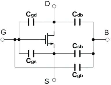
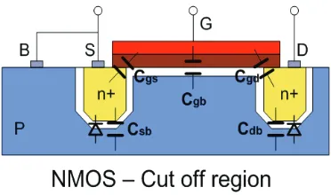
For the case of ISBCs in standard CMOS technology, Cgs , Cgd and Cds are of particular interest. The values of Cgd and Cgs heavily depend on the operation region of the power MOSFET. In this dissertation, when MOSFET works in the cut-off region as illustrated in Figure 2-2, Cgs and Cgd are respectively represented with unit width capacitance (C)
gs
C and (C) gd
C . The values of (C)
gs
C and (C) gd
C satisfy
d ox gso gdo C
gd C
gs C C C C x
C( ) ( ) in which
GDO
C and CGSO are unit width overlap oxide capacitance, Cox is unit width oxide capacitance and xd is called the lateral diffusion coefficient [2-1]. However, when the MOSFET works in the linear region as illustrated in Figure 2-3, Cgsand Cgd are respectively represented with unit width capacitance (L)
gs
C
and (L) gd
C . As gate oxide capacitance should be included, the values of (L) gs
C and (L) gd
C
become L gdo ox eff
gd L
gs C C C L
C( ) ( ) 0.5 where
eff
L is the effective gate length. When the MOSFET works in the saturation region as illustrated in Figure 2-4, Cgsand Cgd are respectively represented with unit width capacitance (S)
gs
C and (S) gd
C . The values of (S) gs
C
and (s) gd
C change to be S gdo ox eff
gs C C L
C
3 2
)
( and
gdo d
gs C
C( ) .
db
C is the junction capacitance and is a value determined by Vds.
Switching losses of the ISBC consist of overlap loss (O-loss), parasitic capacitors charging and discharging loss (C-loss) and gate driver dynamic loss (D-loss).
2.1.1 Present state of switching loss analysis
There are hundreds of papers and application notes that discuss switching loss analysis of discrete synchronous Buck converter (SBC) and the representative papers include [2-2] [2-3] [2-4] [2-5] [2-6] [2-7] [2-8] [2-9] [2-10] [2-11] [2-12] [2-13] [2-14] [2-15] [2-16]. There are also many papers focused on ISBCs [2-17] [2-18] [2-19] [2-20] [2-21] [2-22] [2-23] [2-24] [2-25].
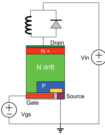
All of these papers adopted a common approach to investigate the switching losses in a Figure 2-4. Cross section of NMOS working in the saturation region
The common approach for the switching loss analysis consists of two steps. Parameters of the power FET are measured via experiment or simulation in the first step. Time domain behaviors of the ISBC in a switching transient are analytically investigated and the switching loss is calculated using the measured power FET parameters in the second step.
The assumptions behind the approach include that all power FET subcells parasitic capacitors are assumed to be identical and the flowing directions of charging/discharging currents in all power FET subcells are the same.
2.1.1.1 Power FET parameters measurement
The values of gate charge Qg, parasitic capacitance Cgd, Cgs and Cdb are usually used to calculate the switching losses. However, the values of Cgd, Cgs and Cdb cannot be directly measured via experiment and are in fact derived from three other measurable parameters including Ciss, Coss and Crss [2-26]. Ciss is defined as the input capacitance of the power FET and Ciss Cgs Cgd; Coss is defined as the output capacitance and
ds gd
oss C C
P N+
N drift
N + Drain
Gate
Source
Vgs
Vin
2.1.1.2 Power FET time domain behavior based switching loss calculation
Switching waveforms of a practical ISBC product are complicated due to the existence of various kinds of parasitic components. In present, there are two typical ways to calculate the switching loss.
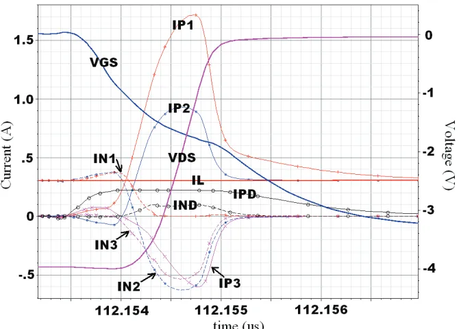
The first typical way [2-12] simplifies the waveforms as piecewise linear ones so that the switching loss calculation becomes straight. Figure 2-7 illustrates the waveforms which are simplified from the experimental observation and can concisely explain the time domain behavior of the power FET during switching transient.
During the time interval t1, the power FET transits from cut-off region to the saturation region. The gate voltage of the power FET increases linearly until it reaches a Miller plateau voltage and the input capacitance Ciss is partially charged. The Ids current of the FET linearly increases too until it equals the total inductor current. During the time t2, the power FET transits from saturation region to linear region. The reverse transfer capacitance Crss and the output capacitanceCoss are completely charged and the gate voltage remains constant as the Miller plateau voltage. The vds of the power FET linearly decreases until it equals the times of rdson and inductor current which approximately
approaches zero. During the time t3, the power FET works in linear region. The input capacitance Ciss charging continues until it is complete and the gate voltage equals vdd. Similar discharging process happens in the time periods t4, t5 and t6 when the power FET is turned off.
Figure 2-7 provides a straight way to calculate the switching loss. The values of t1, t2, and t3 can be calculated with the parameters in datasheet to conclude the switching loss during the power FET turn-on. So do the values of t4, t5, t6 and the switching loss during turn-off process.
Another typical way [2-3, 2-4] addresses the dynamic analysis of ISBC’s switching behavior via building up the RLC equations of the ISBC during switching transient. The parameters Cgd, Cgs and Cdb obtained from datasheet are used in the switching loss analysis. Also, the developed equations are expected to conclude time domain behaviors similar to the experimental switching waveforms.
2.1.1.3Assumptions violation
The present switching loss analysis methods have two assumptions. The first one is that all power FET subcells parasitic capacitors are assumed to be identical; the second one is that the flowing directions of charging/discharging currents in all power FET subcells are assumed to be the same.
The two assumptions are violated when the power width segmentation technique discussed in subsection 1.2.4.4 is adopted for the sake of light load efficiency.
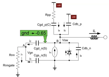
Figure 2-9. Parasitic capacitors in ISBC with two active power FET subcells.
Contr
oller