thermal processing
G. Lucovskya)
Departments of Physics, Materials Science and Engineering, and Electrical and Computer Engineering, North Carolina State University, Raleigh, North Carolina 27695
H. Niimi
Department of Materials Science and Engineering, North Carolina State University, Raleigh, North Carolina 27695
Y. Wu, C. R. Parker, and J. R. Hauser
Department of Electrical and Computer Engineering, North Carolina State University, Raleigh, North Carolina 27695
~Received 3 February 1998; accepted 9 March 1998!
This article addresses several aspects of nitrogen atom ~N atom! incorporation into ultrathin gate oxides including: ~i! monolayer incorporation of N atoms at the Si–SiO2 interfaces to reduce tunneling currents and improve device reliability; and~ii!the incorporation of silicon nitride films into stacked oxide–nitride ~ON! gate dielectrics to ~a! increase the capacitance in ultrathin dielectrics without decreasing film thickness, and~b!suppress boron atom~B atom!diffusion from
p1polycrystalline Si gate electrodes through the dielectric layer to the Si substrate channel region. The results of this article demonstrate that these N-atom spatial distributions can be accomplished by low thermal budget, single wafer processing which includes~i!low-temperature~300 °C!plasma assisted oxidation, nitridation, and/or deposition to achieve the desired N-atom incorporation, followed by~ii!low thermal budget~30 s at 900 °C!rapid thermal annealing to promote chemical and structural bulk and interface relaxation. © 1998 American Vacuum Society.
@S0734-2101~98!58403-5#
I. INTRODUCTION
As the lateral dimensions of advanced Si field effect tran-sistors ~FETs! shrink into the deep submicron range (d
,0.25nm), the oxide equivalent thickness ~tox eq! of gate dielectrics must decrease proportionally into an ultrathin re-gime ~tox eq ,3 nm! in which direct tunneling becomes an important factor in the off-state leakage current. It has been demonstrated that N atoms can be incorporated into ultrathin gate dielectrics by ~i! thermal, ~ii! rapid thermal, and ~iii! plasma-assisted processing.1–3Interfacial N-atom incorpora-tion has been shown to improve device reliability.4 Incorpo-ration of nitrogen in the bulk of the dielectric film in nitride layers has been shown to promote values of tox eqthat are less than the physical thickness of the stacked dielectric as in ONO structures.5 Finally, N-atom incorporation at the top surface of oxide dielectrics has been demonstrated to sup-press B-atom penetration from p1 polysilicon gate electrodes.6,7
This article describes a novel plasma-assisted process for N-atom incorporation at Si–SiO2 interfaces, and demon-strates that dielectrics with nitrided interfaces prepared in this way display reduced tunneling currents. The article also describes new results relative to the preparation and charac-terization of silicon nitride films prepared by remote plasma-assisted deposition. These films have been incorporated into
n-channel FET devices with stacked ON dielectrics.8 The performance of these FETs with stacked ON gate dielectrics
is compared with FETs with oxide dielectrics with the same
tox eq. The suppression of B-atom diffusion from p1 poly-crystalline silicon gate electrodes and accompanying im-provements in device reliability are demonstrated for ultra-thin nitride films, tn;0.8 nm incorporated into stacked ON
dielectrics.7
II. DEVICE FABRICATION
A. Nitrided interfaces
It was previously shown that interface nitridation by plasma-assisted processing could be accomplished by a 300 °C plasma-assisted oxidation process in which N2O was used as the source gas for both initial oxide growth and in-terface nitridation.3,4 This process is the first of a two-step plasma process that has been used to fabricate device quality gate dielectrics.9 The second plasma processing step is a 300 °C remote plasma-assisted deposition of an oxide,3,4,9or a stacked ONO,5or ON structure.7,8To obtain device quality performance and reliability, a post deposition rapid thermal anneal ~RTA! at 900 °C for 30 s was required to promote bulk dielectric and interfacial chemical and structural relax-ations, e.g., to evolve hydrogen from both oxide and nitride dielectrics and to reduce interfacial suboxide bonding.10This article describes an alternative plasma-assisted oxidation/ nitridation process.
dilute HF that~i!removes a thin sacrificial oxide layer and ~ii!produces a hydrogen atom~H atom!terminated surface, the first step in the process is a remote plasma-assisted oxi-dation ~RPAO! using excited species ~e.g., O2*! extracted from a remote He/O2plasma.
3,9,10
This step~i!accomplishes an in situ clean that reduces carbon and fluorine atom contamination,3 ~ii! forms a Si–SiO2 interface, and ~iii! grows;0.5 nm of SiO2which serves as a substrate layer for the deposition of a dielectric film. The 0.5 nm oxide film also prevents further oxidation of the Si substrate during plasma-assisted deposition of oxide layers.9 Interface nitridation is accomplished before deposition of the dielectric by exposure to the products from a remote He/N2 plasma, primarily neu-tral N atoms.11Systematic changes in the NKLLfeature of the AES spectra in Fig. 1 demonstrate that the N-atom concen-tration in the dielectric increases with increasing plasma ex-posure time. Quantification of the rate at which N atoms are introduced in the dielectric will be discussed in the next sec-tion, where additional results from secondary ion mass spec-trometry~SIMS!studies are presented.
Device structures were fabricated on these nitrided oxide interfacial oxide layers by completing the following addi-tional steps: ~i! 300 °C plasma-assisted deposition of SiO2 from remote plasma excitation of a He/O2 and downstream injection of SiH4,3,9,10 ~ii! a 30 s 900 °C rapid thermal anneal,10 ~iii! formation of MOS capacitors using conven-tional photolithographic techniques following either ~a! physical vapor deposition~PVD!of aluminum~Al!contacts, or~b!chemical vapor deposition, doping, and dopant activa-tion of n1 polycrystalline silicon contacts. Following elec-trode deposition, there was a conventional 30 min postmet-allization anneal~PMA!at 400 °C in a forming gas (H2/N2) mixture. Interface characterization and device results are pre-sented in Sec. III A.
performance in devices with ONO structures was used in the nitride deposition step.11Device results are presented in Sec. III C following a discussion of the unique properties of the plasma deposited nitride films in Sec. III B.
The MOS capacitors for the B-diffusion studies were fab-ricated on 5Vcm~100!n-type Si substrates with previously
grown oxide gate dielectrics.7Gate oxides in the range from ;3 to;6 nm were grown by furnace oxidation in dry O2 at 800 °C. This was followed by deposition of nitride films 0.4–0.8 nm thick by 300 °C remote plasma-assisted process. The nitride layer thickness estimated by on-line AES, and confirmed by spectroscopic ellipsometry. The nitride deposi-tion was followed by a 30 s 900 °C RTA. Undoped polycrys-talline silicon, prepared by a conventional low pressure chemical vapor deposition ~LPCVD! process with a thick-ness of;200 nm, was deposited following the gate dielectric RTA. Boron implantation into the polysilicon was performed at 12 keV to a dose of 531015 cm22; this was followed by an aggressive drive-in anneal in argon for 4 min at 1000 °C which activated and redistributed the implanted B atoms. MOS capacitors for electrical testing were completed by con-ventional metallization, patterning and postmetallization an-nealing processes. Electrical results for these PMOS device structures are presented in Sec. III D.
III. EXPERIMENTAL RESULTS
A. Interface characterization and tunneling studies
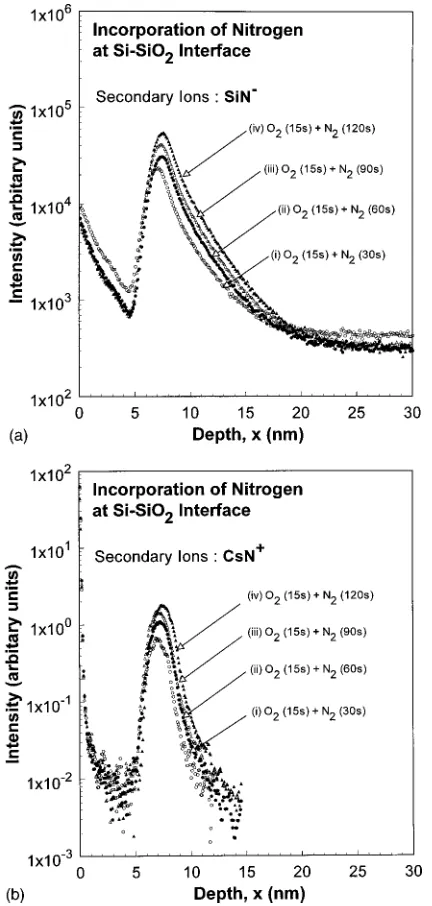
Figures 2~a! and 2~b! present the results of SIMS mea-surements made at Evans East on a stacked dielectric com-prised of the nitrided interface and template film,;0.5–0.6 nm thick, and a ;5 nm plasma-deposited SiO2 film. The nitrided interface then is;5.5–6 nm below the film surface. The SIMS determination of N was made by counting both SiN2and CsN1ions during the sputtering process. The pro-files of these ions indicate that the N atoms are incorporated in the immediate vicinity of the Si–SiO2 interface, and dif-ferences in the profiles are associated with the drive-in of the N atoms into the Si substrate during the SIMS measure-ments. Figures 3~a! and 3~b! indicate that the normalized SIMS signals of Figs. 2~a! and 2~b!, respectively, display a linear dependence as function of nitridation time. In addition, based on normalization procedures discussed in Ref. 3, the FIG. 1. Derivative AES spectra for interface nitridation times of 30, 60, 90,
interface concentration of N atoms attains a monolayer cov-erage ~610%! after a 90 s exposure to the He/N2 plasma process described above.
Figure 4 contains a plot of the ratio of the amplitudes of NKLLand substrate SiLVV~91 eV!features versus nitridation time. A plot of the NKLL strength versus time shows a sub-linear dependence. However, plotting the data as a ratio also yields a linear dependence of the nitrogen concentration ver-sus nitridation time. The use of the N/Si ratio demonstrates that the N atoms are at the Si–SiO2 interface, which is then more accurately characterized as a Si–N–SiO2 interface. Since the 91 eV SiLVV features comes from the substrate, normalization of the NKLL signal takes into account passage of the NKLL electrons through the oxide film, and the
in-crease in overall film thickness as N atoms are incorporated at the Si–SiO2 interface. Note that the escape depth for AES electrons with energies of 90 eV is approximately 0.6 nm. Since the SIMS data indicate a linear dependence of N-atom incorporation with time, the normalized plotting of the AES data establishes the N atoms are at the interface, rather than in the bulk of the plasma grown oxide layer.
Figures 5~a! and ~b! are current density–voltage ~J – V!
plots for the MOS capacitors with nitrided interfaces and
n-type substrates described in Sec. II A. The plot in Fig. 5~a! is for an oxide thickness of ;5 nm. This sample has an Al gate electrode, and the J – V plot is for substrate injection. The current below about 3 V is displacement current associ-ated with the ramped voltage that was used in the J – V data acquistion. The tunneling currents for voltages approxi-FIG. 2. SIMS data on nitride interfaces as a function of nitridation time~see
Fig. 1!, by detection of~a!SiN2ions and~b!CsN1ions. The strong rise of the N-signal marks the interface between the dielectric and a crystalline Si substrate.
FIG. 3. Normalized plots of integrated ion counts vs time:~a!SiN2ions and
mately 3 V and above are associated with a Fowler– Nordheim tunneling process. These tunneling currents de-crease as the time of nitridation inde-creases, and hence as the interfacial nitrogen concentration increases. For a fully-nitrided interface, the tunneling current is reduced by ap-proximately an order of magnitude by the interface nitrida-tion with respect to a non-nitrided interface. Similar reductions in tunneling current density are also observed for direct tunneling as in Fig. 5~b!which displays J – V plots for oxide thickness of approximately 2 and 3.0 nm. These samples have n1 polycrystalline Si gate electrodes and the
J – V plots are also for substrate injection. It is important to
note that the flat-band voltages for the MOS structures of Figs. 5~a!and 5~b!, do not vary by more than 0.05 eV, so that the changes in the J – V plots represent decreased current flow, and are not a result of differences in zero-bias built-in electric fields. Finally, similar results have been obtained for samples with p-type substrates and oxide thicknesses of ;5 nm. For these samples, tunneling currents for gate injection were also reduced by approximately a factor of 10 as inter-face nitridation increased to the ones monolayer level. As in the case of the MOS devices prepared on n-type substrates, the flat-band voltages for the MOS capacitors prepared on
p-type substrates also displayed a change of no more than
;0.05 eV between the non-nitrided and fully-nitrided inter-faces.
B. Characterization of plasma deposited nitrides
The hydrogenated plasma deposited nitrides have been characterized by infrared~IR!absorption measurements.12IR spectra indicated features due to: ~i! the Si–N asymmetric bond-stretching vibration at ;850 cm21; ~ii! the bond-stretching vibration of the N–H group at ;3350 cm21;~iii! the bond-bending vibration of the N–H group at ;1150
cm-1, and ~iv! the bond-stretching vibration of the Si–H group at ;2170 cm21. Films deposited at 300 °C from dif-ferent source gas mixtures of NH3/SiH4 established that be-ginning at about 400 °C hydrogen was evolved from the film. The loss of H atoms could be described by a temperature-activated process with an activation of ;0.4 eV. This was consistent with H-atom loss being associated with processes in which molecular H2 was formed. For example, it was FIG. 4. Plot of the ratio of the amplitudes of NKLLand substrate SiLVV~91
eV!features vs nitridation time.
demonstrated that the hydrogenated silicon nitride films con-tained nearest-neighbor Si–H—H–N–Si bonding arrange-ments, and that there were significant decreases in the both the Si–H and N–H vibrational signatures with annealing.12,13 A reaction pathway for H-atom evolution that is suggested by these results is
Si–H—H–N–Si→Si010N–Si1H2, ~1!
where the superscript notation (0) indicates a neutral dan-gling bond, and the H—H notation indicates nearest network neighbors. In the temperature range to about 500–600 °C, the only significant changes in the IR were decreases in the amplitudes of the Si–H and N–H vibrations, whereas at tem-peratures greater than about 600 °C, there was a systematic increase in the amplitude of the Si–N feature. The combina-tion of these results for annealing temperature.600 °C sug-gests that as H atoms were evolved from the films, new Si–N bonds were formed. This is represented symbolically in Eqs. ~2a!and~2b!:
Si–H—H–N–Si→Si010N–Si1H2, ~2a!
Si010N–Si→Si–N–Si. ~2b!
The as-deposited films also contain SiNH groups in two other bonding arrangements: ~i! in nearest-neighbor pairs, where they interact via H-bonding interactions, and ~ii! as isolated bonding groups where the H atoms of the N group interact with near-neighbor N atoms of the network. The interactions in~ii!are also H-bonding-type interactions, and the distribution of near-neighbor N atoms is determined by the local network bonding at the particular N–H site. Loss of hydrogen with the subsequent evolution of different N–H bonding groups such as N–H2 can occur from the nearest neighbor pairs, with reaction pathways being similar to those described in Eqs. ~1! and ~2!. Loss of H atoms from the isolated N–H groups is considerably less likely due to the relatively high N–H bond energy, of the order of 5 eV.
As noted in Sec. II, a source gas ratio of NH3:SiH4 of ;10:1 gave optimum electrical performance. Combining IR and AES data with a statistical model of bonding in amor-phous Si:N:H alloys indicates that this source gas ratio
cor-responds to a film in which the respective silicon, nitrogen, and hydrogen concentrations are @Si# ;28 at. %, @N# ;42 at. %, and@H# ;30 at. %14It was shown in Ref. 14, that the average number of bonds/atom for this composition is;2.7, the same as in device-quality plasma-deposited SiO2 films. In addition, hydrogenated silicon nitride films with this com-position have been used in amorphous silicon thin film tran-sistors as the gate dielectrics and yielded optimized electrical performance. For example, transconductance electron mo-bilities of ;1.5 cm2V21 s21 15 were obtained indicating a low concentration of charged defect centers. For both lower and higher source gas ratios, the film composition changed and the effective channel mobility decreased. This behavior has been interpreted as being a manifestation of the similar-ity in bonding statistics to SiO2as noted earlier in this para-graph.
C. Electrical performance of FETs with ON dielectrics
Figures 6~a!and 6~b!present data on the performance and reliability of FETs incorporating stacked ON gate dielectrics.8These data have been discussed in more detail in Ref. 8. In summary, the approximate electrical thickness of the gate dielectrics was obtained to 61 Å from analysis of capacitance–voltage ~C – V! data. TEM micrographs of the composite ON structures indicated approximately equal ox-ide and nitrox-ide layer thickness. Based on an approximately 1:2 ratio of silicon nitride to silicon oxide static dielectric constants, this means that a 1.860.1 nm ON film is com-prised of oxide and nitride layers which are each approxi-mately 1.260.1 nm thick. The transistor characteristics, drain current, Id, versus drain bias voltage, Vd, plotted for
different normalized gate voltages (Vg2Vth, where Vgis the
gate voltage and Vthis the threshold voltage!. Since the Id is
~ ! MOS capacitors ~i! with a control thermal oxide, and ~ii! with composite oxide–nitride dielectrics with 0.4 nm, and 0.8 nm thick nitride layers. The C – V curve for the control oxide shifted significantly to a relatively high flatband volt-age, VFB,as compared to nitride-deposited devices indicating a large amount of B atom penetration has occurred. This was confirmed by preparing capacitors with Al gate electrodes on the different gate dielectrics used above, i.e., the control ther-mal oxide, and the composite oxide–nitride dielectrics. The flatband voltages for these NMOS structures were obtained from C – V measurements and were also essentially the same,
20.8260.1 V. Using these results enabled us to determine an anticipated value for using a B-atom doped polycrystal-line Si gate electrode in a PMOS structure. One of the most important aspects of this comparative study on NMOS struc-tures was the consistency of the flatband voltages for the different gate dielectric structures. This consistency means that introducing the nitride films on the oxide substrate did not introduce fixed charge at either the Si–SiO2 interface, or the internal interface between the nitride and oxide constitu-ents of the dual layer dielectrics similar to what had been found in our earlier studies tri-layer oxide–nitride–oxide di-electrics which were made using essentially the same se-quence of plasma and rapid thermal annealing process steps.15 The anticipated VFB is approximately 10.7 V, and
VFBfor the control oxide is shifted to approximately11.1 V. The VFBvalue for the capacitor with the 0.8 nm nitride is at approximately 10.7 eV indicating essentially no boron pen-etration to the underlying n-type Si substrate. VFB for the device with the 0.4 nm top nitride is intermediate, approxi-mately10.8 V, which shows the degree of boron penetration is controllable for a fixed thermal budget by changing the deposited nitride layer thickness. Oxide reliability was exam-ined by measuring charge to breakdown (QBD) under con-stant Fowler–Nordheim current stressing as shown in Fig. 7~b!. Each experimental point is the average of 15 device runs. QBDwas highest for film with the thickest top nitride layer. The relative decreases in QBDin capacitors with the control oxide, and the composite dielectric with the 0.4 nm nitride layer are attributed to boron penetration. The QBD value of the capacitor with the 0.8 nm top nitride is twice as high as that of the capacitor with the control oxide. As a point for reference, the QBDvalues for MOS capacitors with Al-gate electrodes were found to be essentially the same as that of the capacitor with the dual layer oxide–nitride
dielec-tric with the 0.8 nm nitride. Figure 7~c! shows applied gate voltages shifts as a function of injected charge. The reliabil-ity of the devices with the top surface nitride layers is clearly improved.
FIG. 7. Date for PMOS devices with;5–6 nm dielectrics:~a!Normalized quasistatic C – V curves for MOS capacitors with different thickness of top nitride layers: tn50.0, 0.4, and 0.8 nm;~b!charge to breakdown~QBD!for 50% failure under constant current substrate injection at 100 mA cm22; and
IV. DISCUSSION
This section is divided into three parts which address, respectively: ~i!the reduction of tunneling currents in MOS capacitors with nitrided interfaces; ~ii!the unique character of the nitride films formed by the two step process sequence of 300 °C deposition by remote plasma-assisted deposition followed by a vacuum or inert ambient RTA for 30 s at 900 °C; and ~iii! the suppression of nitrogen diffusion through ultrathin nitride layers.
A. Nitrided interfaces
The J – V data in Figs. 5~a!and 5~b!in Sec. III A indicate significant decreases in tunneling current density with in-creasing interface nitridation. At first sight this result is sur-prising since the Si–SiO2 conduction band off-set energy is significantly higher than the Si–Si3N4 conduction band off-set energy,;3.1 eV as compared to 2.1 eV,16suggesting that interfacial nitridation would be expected to increase tunnel-ing currents. The nearly constant reduction of tunneltunnel-ing cur-rent for thicknesses in the Fowler–Nordheim regime as in Fig. 5~a!, and in the direct tunneling regime as in Fig. 5~b!, as well as the fact that similar reductions occur for both substrate and gate injection, indicates that the reduction is not simply due to changes in effective oxide thickness, or the direction of current injection. Flat-band voltages, obtained from analysis of C – V curves have indicated a small varia-tion of flat-band voltage with interface nitridavaria-tion~,0.05 V!, demonstrating that built-in oxide fields were not the cause of the current reductions. In addition, a newly developed model for band off-set energies that includes the effects of charge transfer interface dipoles places an upper limit on the pos-sible flat band voltage shifts17 of ;0.1 eV that supports to the results of the C – V and J – V studies.
Studies of Si–SiO2interfaces have shown that the oxida-tion of Si invariably results in transioxida-tion regions with excess suboxide bonding between the crystalline Si substrate and the SiO2.
18
IfFmsis the metal-semiconductor work function in the absence of interfacial dipoles, then the effective metal-semiconductor work function for a non-nitrided interface with interfacial Si–O bonds, Fms
8
~Si–O!, is given by:Fms
8
~Si–O!5Fms2Vdipole~Si–O!, ~3! where Vdipole~Si–O! is the potential energy step associated with interfacial dipoles. This potential energy step adds to the conduction band offset as determined from vacuum lev-els. In Ref. 17, it is demonstrated that Vdipole~Si–O!depends on the nature of the bonding at the Si–SiO2 interface. The dipole step is greater for an abrupt Si–SiO2 interface,Vdipole~Si–Oabrupt), than for an interface with suboxide bond-ing, Vdipole(Si–Osuboxide). In addition, it was shown that the dipole step is greater for a nitrided Si–N–SiO2interface than for an interface with significant suboxide bonding as has been reported for Si–SiO2interfaces even after a 30 s 900 °C RTA. The difference in the height of the potential barrier between a nitrided interface and an interface with suboxide bonding is given by
dV5Vdipole~Si–N!-Vdipole~Si–Osuboxide!. ~4!
The calculations of Ref. 18 show thatdV at most equal to 0.1
eV so that the barrier height is not significantly different for an abrupt nitrided interface and for a Si–SiO2 interface that has a minimized degree of suboxide bonding after a 900 °C RTA. The driving force for dipole formation is an equaliza-tion of a chemical potential that can be obtained from con-siderations of the relative electronegativities of the interfacial bonding arrangements. Under this driving force, electrons are transferred from the Si substrate to the dielectric. The magnitude of the charge transfer is ;0.1–0.2e, where e is the charge on the electron.17 This analysis supports the re-sults of the C – V and J – V measurements of Sec. III A; i.e., that the changes in tunneling currents are not due to system-atic changes in built in fields, associated with changes in flat band voltages.
Therefore, an alternative mechanism must be invoked to explain the tunneling results. One way to interpret the data in Figs. 5~a!and 5~b!, as well as the additional results for the
p-type substrate, is to invoke an interfacial reflection coeffi-cient that is significantly different for non-nitrided and
fully-nitrided Si–SiO2 interfaces. One rationale for this type of effect has its origin in effects well-known in physical optics, where thin surface layers of transparent materials with dif-ferent optical indices of refraction will either enhance or duce surface reflectivity, and thereby reduce or enhance, re-spectively, the optical transmission independent of the surface on which the light is incident. The optical path length for these surface layers must be in the range of about one-quarter of the optical wavelength in the surface layer mate-rial. For this type of mechanism to apply to the nitrided oxide dielectrics, the monolayer nitridation would have to have an effective index of refraction higher than that of the oxide surface. Stated differently, the reduced tunneling mechanism would have to rely on a significant phase shift for the electron transport in the nitrided layer relative to that of the non-nitrided interface. This type of contribution to the tunneling transport needs additional theorectical and experi-mental study.
tive charge, i.e., reductions in defects in the nitride film. Therefore this figure demonstrates that the formation of ad-ditional Si–N bonds from bonding groups that have loose H atoms is responsible for the improved behavior.
To best understand the unique attributes of the two-step process for forming device-quality nitride films with low bulk defect densities, it is necessary to contrast the bonding changes that take place in these films as a function of pro-cessing, with the bonding in nitride films prepared by con-ventional higher temperature~T.500 °C!LPCVD processes. Summarizing the IR data presented above: ~i! as-deposited silicon nitride films are Si:N:H alloys with an average num-ber of bonds/atom ~;2.7! which is essentially the same as deposited SiO2; ~ii!these films are therefore low defect con-tinuous random network structures with low bulk defect den-sities, primarily because of their high H-atom content~;30 at. %!;~iii!these films contain several kinds of bonded H:~a! in nearest-neighbor SiH/SiNH and SiNH/SiNH pairs, and~b! in isolated SiNH groups;~iv!upon annealing to 500 °C, H is released from these nearest-neighbor groups leading to de-fect formation as both Si- and N-atom dangling bonds; ~v! upon further annealing at temperature.500 °C, H evolution continues, but additional Si–N bonds are formed; ~vi! the formation of additional Si–N bonds from bonding sites that have lost H atoms reduces bulk defect densities accounting for the unique electrical properties of the films. In effect the special bonding arrangements in which H atoms are nearest-network neighbors in the as deposited films is the key to the unique behavior. For example, these bonding sites are the reason for poor performance in films annealed to 500 °C, but are the reason for improvements in performance in films that have been annealed to 900 °C. The IR spectra of Ref. 12 clearly indicate that additional Si-N bonds are formed after the 900°C anneal; however, at this time we offer no micro-scopic model for the atomic motions that are involved in these relaxation processes.
It is found in Ref. 12 that the nitride films contain bonded hydrogen after 900 °C. This is mostly in isolated bonding arrangements in SiNH bonding arrangements. The bonding energy of the HN bond in a SiNH group is in excess of 5 eV. As an isolated bonding arrangement, this site will not be an electronically active defect, although under certain condi-tions it may act as a defect precursor. One pathway for defect generation is through hole trapping and the formation of an ammonium center. However, at the low bias voltages that are
duced at lower temperature by remote plasma processing, and therefore the films have high defect densities even after higher temperature processing. The only way that defects in these films can be reduced in density is by postdeposition annealing in an oxygen containing ambient as shown by the recent results reported by the University of Texas at Austin Group.19 Films prepared in this way are oxynitride alloys with dielectric constants below those of silicon nitride. Ox-ynitride alloy films have been incorporated into FETs, but in general this leads to significant reductions in peak channel mobilities in NMOS devices.20
C. Stopping power of nitride layers for B-atom diffusion
The stopping power of nitride films prepared by remote plasma processing and subsequent RTAs is simply associ-ated with the high areal density of N atoms obtained in this way. The areal density of N atoms in a film that is 0.8 nm thick is estimated to be 4 – 531015 cm22.7Since the bond-ing radius of N atoms is;0.8 nm, this means that the frac-tional area coverage of these N atoms is ;0.8–1.0. Since it has been shown that the diffusion of B atoms through oxide films involves B–O bond formation, the 0.8 nm nitride film effectively screens the B atoms from the O atoms in the underlying oxide film of the stacked ON dielectric.21 Reduc-ing the nitride thickness to ;0.4 nm reduces the fractional coverage to 0.4–0.5, enabling the B atoms to interact with the underlying oxide layer, and be transported to the Si sub-strate where they can degrade electrical performance. As an-ticipated, increasing the nitride layer to 1.2 nm, as in the FETs described above will then not only reduce direct tun-neling, but also improve resistance to B-atom penetration in PMOS devices.
V. SUMMARY
be formed. The interface nitridation and ON stacked dielec-trics have been demonstrated to yield improved behavior with respect to ultrathin oxides in NMOS devices with oxide equivalent thickness down to 1.8 nm. Extensions of this ap-proach, based on the calculation of tunneling currents in stacked ON devices suggests that the stacked ON dielectrics can be used for several device generations, in particular for
tox eqextending down to at least 1.5 nm, and perhaps to 1.2 nm. The stacked ON gate dielectrics with at least 0.8 nm of nitride have shown excellent resistance to B-atom transport out of p1 polycrystalline silicon gate electrodes. Since the top surface nitridation process also nitrides the Si–SiO2 interface,22the channel mobilities of holes in PMOS devices may be degraded by the use of these structures.
ACKNOWLEDGMENTS
This work was supported in part by the NSF Engineering Research Center for Advanced Electronic Materials Process-ing at North Carolina State University, the Office of Naval Research, and the Semiconductor Research Corporation.
1
D. Mathiot, A. Straboni, E. Andre, and P. Debenest, J. Appl. Phys. 73, 8215~1993!; J. Ahn, J. Kim, G. Q. Lo, and D.-L. Kwong, Appl. Phys. Lett. 60, 2089~1992!.
2M. L. Green, in Fundamental Aspects of Ultrathin Dielectrics in Si-based
Devices, edited by E. Garfunkel, E. Gusev, and A. Vul~NATO, in press!. 3
D. R. Lee, G. Lucovsky, M. R. Denker, and C. Magee, J. Vac. Sci. Technol. A 13, 1671~1995!.
4D. R. Lee, C. R. Parker, J. R. Hauser, and G. Lucovsky, J. Vac. Sci. Technol. B 13, 1778~1995!.
5Y. Ma, T. Yasuda, and G. Lucovsky, Appl. Phys. Lett. 64, 2226~1994!. 6
S. V. Hattangady et al., Tech. Dig. Int. Electron Devices Meet. 495
~1996!. 7
Y. Wu, G. Lucovsky, and H. Z. Massoud, Proc. IEEE Reliab. Phys. Symp.~in press!.
8C. G. Parker, G. Lucovsky, and J. R. Hauser, IEEE Electron Device Lett.
19, 106~1988!.
9T. Yasuda, Y. Ma, S. Habermehl, and G. Lucovsky, Appl. Phys. Lett. 60, 434~1992!.
10G. Lucovsky, H. Niimi, K. Koh, D. R. Lee, and Z. Jing, The Physics and
Chemistry of SiO2and the Si–SiO2Interface, edited by H. Z. Massoud, E. H. Poindexter, and C. R. Helms~Electrochemical Society, Pennington, NJ, 1996!, p. 441.
11M. Kushner~private communication!. 12
Z. Lu, M. J. Williams, P. F. Santos-Filho, and G. Lucovsky, J. Vac. Sci. Technol. A 13, 607~1995!.
13
G. Lucovsky, P. Santos-Filho, G. Stevens, Z. Jing, and A. Banerjee, J. Non-Cryst. Solids 198-200, 19~1996!.
14G. Lucovsky and J. C. Phillips, J. Non-Cryst. Solids~in press!. 15Y. Ma, T. Yasuda, and G. Lucovsky, J. Vac. Sci. Technol. A 11, 952
~1993!; Y. Ma, T. Yasuda, S. Habermehl, and G. Lucovsky, J. Vac. Sci. Technol. B 11, 1533~1993!.
16
H. Yang, H. Niimi, and G. Lucovsky, J. Appl. Phys. 83,~1998!. 17
G. Lucovsky, H. Yang, and H. Z. Massoud, J. Vac. Sci. Technol. B 16,
~1998!.~1998!. 18
G. Lucovsky, A. Banerjee, B. Hinds, B. Claflin, K. Koh, and H. Yang, J. Vac. Sci. Technol. B 15, 1074~1997!.
19
B. Y. Kim, H. F. Luan, and D. L. Kwong, Tech. Dig. Int. Electron De-vices Meet. 97, 463~1997!.
20E. M. Vogel, Ph.D thesis, Department of Electrical and Computer Engi-neering, North Carolina State University, 1998.
21R. Fair, IEEE Electron Device Lett. 18, 244~1997!.