Available online: http://internationaljournalofresearch.org/ P a g e | 1091
*B. Pravallika
Abstract—In this brief, the logic
operations involved in conventional carry
select adder (CSLA) and binary to
excess-1 converter (BEC)-based CSLA are
analyzed to study the data dependence and
to identify redundant logic operations. We
have eliminated all the redundant logic
operations present in the conventional
CSLA and proposed a new logic
formulation for CSLA. In the proposed
scheme, the carry select (CS) operation is
scheduled before the calculation of
final-sum, which is different from the
conventional approach. Bit patterns of two
anticipating carry words (corresponding to
cin = 0 and 1) and fixed cin bits are used
for logic optimization of CS and
generation units. An efficient CSLA
design is obtained using optimized logic
units. The proposed CSLA design involves
significantly less area and delay than the
recently proposed BEC-based CSLA. Due
to the small carry-
**P. Kiran Kumar
Output delay, the proposed CSLA design
is a good candidate for square-root(SQRT)
CSLA. A theoretical estimate shows that
the proposed SQRT-CSLA involves nearly
35% less area–delay–product (ADP)than
the BEC-based SQRT-CSLA, which is
best among the existing SQRT-CSLA
designs, on average, for different
bit-widths. The application-specified
integrated circuit (ASIC) synthesis result
shows that the BEC-based SQRT-CSLA
design involves 48%more ADP and
consumes 50% more energy than the
proposed SQRT-CSLA, on average, for
different bit-widths.
Index Terms—Adder, arithmetic unit,
low-power design.
I.INTRODUCTION
LOW-POWER, area-efficient, and
high-performance VLSI systems are
increasingly used in portable and mobile
* M.TECH student , Dept of DSCE, Balaji Institute Of Technology And Science
P a g e | 1092
devices, multi standard wireless receivers,
and biomedical instrumentation
[1], [2]. An adder is the main component
of an arithmetic unit. A complex digital
signal processing (DSP) system involves
several adders. An efficient adder design
essentially improves the performance of a
complex DSP system. A ripple carry adder
(RCA) uses a simple design, but carry
propagation delay (CPD) is the main
concern in this adder.
Carry look-ahead and carry select (CS)
methods have been suggested to reduce the
CPD of adders.
A conventional carry select adder (CSLA)
is an RCA–RCA configuration that
generates a pair of sum words and output
carry bits corresponding the anticipated
input-carry (cin =0 and 1) and selects one
out of each pair for final-sum and
final-output-carry [3]. A conventional CSLA has less CPD than an RCA, but the design
is not attractive since it uses a dual RCA.
Few attempts have been made to avoid
dual use of RCA in CSLA design. Kim
and Kim [4] used one RCA and one
add-one circuit instead of two RCAs, where the
add-one circuit is implemented using a
multiplexer (MUX). He et al.[5] proposed
a square-root (SQRT)-CSLA to implement
large bit-width adders with less delay. In a
SQRT CSLA, CSLAs with increasing size
are connected in a cascading structure. The
main objective of SQRT-CSLA design is
to provide a parallel path for carry
propagation that helps to reduce the
overall adder delay. Ram kumar and Kittur
[6] suggested a binary to BEC-based
CSLA. The BEC-based CSLA involves
less logic resources than the conventional
CSLA, but it has marginally higher delay.
A CSLA based on common Boolean logic
(CBL) is also proposed in [7] and [8]. The
CBL-based CSLA of [7] involves
significantly less logic resource than the
conventional CSLA but it has longer CPD,
which is almost equal to that of the RCA.
To overcome this problem, a SQRT-CSLA
based on CBL was proposed in [8].
However, the CBL-based SQRT CSLA
design of [8] requires more logic resource
and delay than the BEC-based
SQRT-CSLA of [6]. We observe that logic
optimization largely depends on
availability of redundant operations in the
formulation, whereas adder delay mainly
depends on data dependence. In the
existing designs, logic is optimized
without giving any consideration to the
data dependence. In this brief, we made an
analysis on logic operations involved in
conventional and BEC-based CSLAs to
study the data dependence and to identify
redundant logic operations. Based on this
analysis, we have proposed a logic
formulation for the CSLA. The main
contribution in this brief is logic
P a g e | 1093
optimized carry generator (CG) and CS
design.
Based on the proposed logic formulation,
we have derived an efficient logic design
for CSLA. Due to optimized logic units,
the proposed CSLA involves significantly
less ADP than the existing CSLAs. We
have shown that the SQRT-CSLA using
the proposed CSLA design involves nearly
32% less ADP band consumes 33% less
energy than that of the corresponding
SQRT-CSLA.
II. LOGIC FORMULATION
The CSLA has two units: 1) the sum and
carry generator unit (SCG) and 2) the sum
and carry selection unit [9]. The SCG unit consumes most of the logic resources of
CSLA and significantly contributes to the
critical path. Different logic designs have
been suggested for efficient
implementation of the SCG unit. We made
a study of the logic designs suggested for
the SCG unit of conventional and
BEC-based CSLAs of [6] by suitable logic
expressions. The main objective of this
study is to identify redundant logic
operations and data dependence.
Accordingly, we remove all redundant
logic operations and sequence logic
operations based on their data dependence.
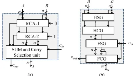
Fig. 1. (a) Conventional CSLA; n is the input operand bit-width. (b) The logic operations of the RCA is shown in split form, where HSG, HCG, FSG, and FCG represent half-sum generation, half-carry generation, sum generation, and full-carry generation, respectively.
A. Logic Expressions of the SCG Unit of
the
Conventional CSLA
As shown in Fig. 1(a), the SCG unit of the
conventional CSLA [3] is composed of
two n-bit RCAs, where n is the adder
bit-width. The logic operation of the n-bit
RCA is performed in four stages: 1)
half-sum generation (HSG); 2) half-carry
generation (HCG); 3) full-sum generation
(FSG); and 4) full carry generation (FCG).
Suppose two n-bit operands are added in
the conventional CSLA, then RCA-1 and
RCA-2 generate-bit sum (s0 and s1) and
output-carry (c0out and c1out)
corresponding to input-carry (cin = 0 and
P a g e | 1094
RCA-1 and RCA-2 of the SCG unit of
then-bit CSLA are given as
As shown in (1a)–(1c) and (2a)–(2c), the
logic expression of {s00(i), c00(i)} is
identical to that of {s10(i), c10(i)}. These redundant logic operations can be removed
to have an optimized design for RCA-2, in
which the HSG and HCG of RCA-1is
shared to construct RCA-2. Based on this,
[4] and [5] have used an add-one circuit
instead of RCA-2 in the CSLA, in which a
BEC circuit is used in [6] for the same
purpose. Since the BEC-based CSLA
offers the best area–delay–power
efficiency among the existing CSLAs, we
discuss here the logic expressions of the
SCG unit of the BEC-based CSLA as well.
B. Logic Expression of the SCG Unit of
the BEC-Based CSLA
As shown in Fig. 2, the RCA calculates n
-bit sum s01and c0outcorresponding to cin
= 0. The BEC unit receives s01and
c0outfrom the RCA and generates (n +
1)-bit excess-1 code. The most significant 1)-bit
(MSB) of BEC represents c1out, in which
nleast significant bits (LSBs) represent
s11. The logic expressions
Fig. 2. Structure of the BEC-based CSLA; n is the input operand bit-width.
of the RCA are the same as those given in
(1a)–(1c). The logic expressions of the
BEC unit of the n-bit BEC-based CSLA
are given as
We can find from (1a)–(1c) and (3a)–(3d)
that, in the case of the BEC-based CSLA,
c11depends on s01, which otherwise has
no dependence on s01in the case of the
conventional CSLA. The BEC method
therefore increases data dependence in the
CSLA. We have considered logic
expressions of the conventional CSLA and
made a further study on the data
dependence to find an optimized logic
expression for the CSLA. It is interesting
to note from (1a)–(1c) and (2a)–(2c) that
logic expressions of s01and s11are
identical except the termsc01and c11since
P a g e | 1095
c01and c11depend on {s0, c0, cin}, where
c0 = c00= c10. Since c01and c11have no
dependence on s01and s11, the logic
operation of c01and c11can be scheduled
before s01and s11, and the select unit can
select one from the set (s01, s11) for the
final-sum of the CSLA. We find that a significant amount of logic resource is
spent for calculating {s01, s11}, and it is
not an efficient approach to reject one
sum-word after the calculation.
Fig. 3. (a) Proposed CS adder design
III. PROPOSED ADDER DESIGN
The proposed CSLA is based on the logic
formulation given in (4a)–(4g), and its
structure is shown in Fig. 3(a). It consists
of one HSG unit, one FSG unit, one CG
unit, and one CS unit. The CG unit is
composed of two CGs (CG0 and CG1)
corresponding to input-carry ‗0‘ and ‗1‘.
The HSG receives two n-bit operands (A
and B) and generate half-sum word s0 and
half-carry wordc0 of width n bits each.
Both CG0 and CG1 receive s0 and c0from
the HSG unit and generate two n-bit
full-carry words c01and c11corresponding to
input-carry ‗0‘ and ‗1‘, respectively. The
logic diagram of the HSG unit is shown in
Fig. 3(b). The logic circuits of CG0 and
CG1 are optimized to take advantage of
the fixed input-carry bits. The optimized
designs of CG0 andCG1 are shown in Fig.
3(c) and (d), respectively. The CS unit
selects one final carry word from the two
carry words available at its input line using
the control signal cin. It selects c01when
cin = 0; otherwise, it selects c11.
The CS unit can be implemented using an
n-bit 2-to-l MUX. However, we find from
the truth table of the CS unit that carry
words c01andc11follow a specific bit
pattern. If c01(i) = ‗1‘, then c11(i) =
1,irrespective of s0(i) and c0(i), for 0 ≤ i≤
n − 1. This feature is used for logic optimization of the CS unit. The optimized
design of the CS unit is shown in Fig. 3(e),
which is composed of n AND–OR gates.
The final carry word c is obtained from the
CS unit. The MSB of c is sent to output as
cout, and (n − 1)LSBs are XORed with (n
− 1) MSBs of half-sum (s0) in the FSG
[shown in Fig. 3(f)] to obtain (n − 1)
MSBs of final-sum(s). The LSB of s0 is
P a g e | 1096
RESULT
V.CONCLUSION
We have analyzed the logic operations
involved in the conventional and
BEC-based CSLAs to study the data dependence
and to identify redundant logic operations.
We have eliminated all the redundant logic
operations of the conventional CSLA and
proposed a new logic formulation for the
CSLA. In the proposed scheme, the CS
operation is scheduled before the
calculation of final-sum, which is different
from the conventional approach. Carry
words corresponding to input-carry ‗0‘ and
‗1‘generated by the CSLA based on the
proposed scheme follow a specific bit
pattern, which is used for logic
optimization of the CS unit. Fixed input
bits of the CG unit are also used for logic
optimization. Based on this, an optimized
design for CS and CG units are obtained.
Using these optimized logic units, an
efficient design is obtained for the CSLA.
The proposed CSLA design involves
significantly less area and delay than the
recently proposed BEC-based CSLA. Due
to the small carry output delay, the
proposed CSLA design is a good candidate
for the SQRT adder. The ASIC synthesis
result shows that the existing BEC-based
SQRT-CSLA design involves 48% more
ADP and consumes 50% more energy than
the proposed SQRTCSLA, on average, for
different bit-widths.
REFERENCES
[1] K. K. Parhi, VLSI Digital Signal
Processing. New York, NY, USA:Wiley,1998.
[2] A. P. Chandrakasan, N. Verma, and D.
C. Daly, ―Ultralow-power electronicsfor
biomedical applications,‖ Annu. Rev.
Biomed. Eng., vol. 10, pp. 247–274, Aug. 2008.
[3] O. J. Bedrij, ―Carry-select adder,‖ IRE
Trans. Electron. Comput.,vol. EC-11, no. 3, pp. 340–344, Jun. 1962.
[4] Y. Kim and L.-S. Kim, ―64-bit
carry-select adder with reduced area,‖Electron.
Lett., vol. 37, no. 10, pp. 614–615, May 2001.
[5] Y. He, C. H. Chang, and J. Gu, ―An
area-efficient 64-bit square root
carryselectadder for low power
application,‖ in Proc. IEEE Int. Symp.
CircuitsSyst., 2005, vol. 4, pp. 4082–4085. [6] B. Ramkumar and H.M. Kittur,
―Low-power and area-efficient
carry-selectadder,‖ IEEE Trans. Very Large
P a g e | 1097
[7] I.-C. Wey, C.-C. Ho, Y.-S. Lin, and C.
C. Peng, ―An area-efficient carryselect
adder design by sharing the common
Boolean logic term,‖ in Proc.IMECS,
2012, pp. 1–4.
[8] S.Manju and V. Sornagopal, ―An
efficient SQRT architecture of carry
selectadder design by common Boolean
logic,‖ in Proc. VLSI ICEVENT, 2013,pp.
1–5.
[9] B. Parhami, Computer Arithmetic:
Algorithms and Hardware Designs,2nd ed. New York, NY, USA: Oxford Univ. Press,