1736 | P a g e
Ab Initio Study of Structural and Electronic Properties of
GaP and Ga
0.875
Fe
0.125
P using First Principle Calculations
Kirandish Kaur
1, Anita Rani
2*Guru Nanak College for Girls, Sri Muktsar Sahib, 152026, Punjab,( India)
ABSTRACT
We investigated the structural and electronic Properties of GaP and Ga0.875Fe0.125P diluted Magnetic Semiconductor in Zinc Blende (B3) phase. The calculations have been performed using Density functional
theory as implemented in the Spanish Initiative for Electronic Simulations with Thousands of Atoms code using
local density approximation as exchange-correlation (XC) potential. The calculated spin polarized energy band
structures show that Ga0.875Fe0.125P is metallic in nature for both spin up and spin down states. Calculated results are also compared with available previous theoretical and experimental.
I. INTRODUCTION
Modern technology of spintronics i.e. spin based electronics is based on the spin of charge carriers and play
wonderful role in emerging field of new multi-functional devices [1-5]. The semiconductors formed from
elements of groups III and V have important properties and have important place in semiconductor industry.
Due to this, the study of these materials and ternary alloys of such materials i.e. dilute magnetic semiconductors
(DMS) attracts a lot of attention of researchers in experimental as well as theoretical field. [6-8]. Doping of
transition metal atoms in GaP has been under research due to its interesting properties that may contribute in the
development of spintronic appliances [9-17].
II. COMPUTATIONAL METHOD
In our research paper, we have studied structural and electronic properties of pure GaP and Ga0.875Fe0.125P using
Density Functional Theory as implemented in SIESTA (Spanish Initiative for Electronic Simulations with
Thousands of Atoms) code [18]. We have used Local Density Approximation (LDA) parameterized by CA as
exchange correlation potential [19]. The structural parameters including Lattice constants within the range of
experimental values, mesh cut-off are optimized to the equilibrium total energy. Using 2 1 1 dimension
standard sixteen atoms per supercell and substituting the Gallium atom at (0, 0, 0) position with Fe atom,
constructed the crystal structures of Ga0.875Fe0.125P under discussion. Including semi-core Fe-3d states as valence
electrons in our calculations, we have generated norm-conserving pseudopotentials in the manner of Troullier
and Martins [20]. An energy shift of 80 meV and Double zeta polarization (DZP) basis set is used for these spin
1737 | P a g e
III. RESULT AND DISCUSSION
3.1. Structural Properties
In this paper, we have studied the zinc blende structure of GaP and Ga0.875Fe0.125P. We investigated the total
energy values for several values of lattice constants in the range of lattice constant of pure GaP [21]. For
structural optimization Murnaghan's equation [22] of state is used by minimizing the total energy with respect to
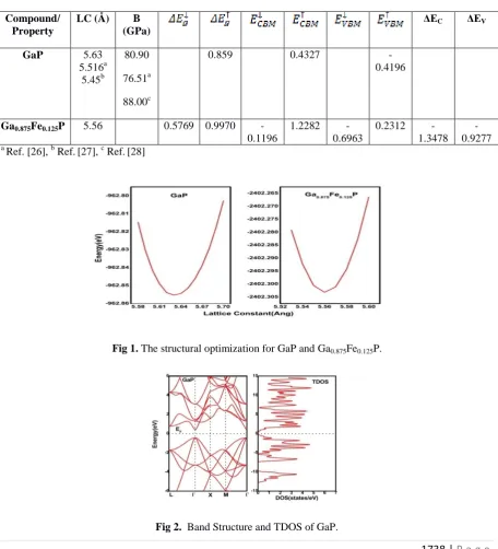
unit cell volume. Figure 1 represents the structural optimization for GaP and Ga0.875Fe0.125P compounds and
these optimized lattice parameters are further used to study the detailed analysis of electronic properties of
compounds under discussion. On replacement of one Ga atom with Fe metal atom, we observe a small
decrement in lattice constant value. This is explained on the basis that atomic size of Fe is less than the Ga
because of increased nuclear attraction for valence electrons in case of Fe.
3.2. Electronic Properties:
Calculated spin polarized energy band structures along with TDOS of pure GaP and Ga0.875Fe0.125P are shown in
Fig. 2 and Fig. 3 respectively. The detailed analysis of these structures show that on doping of Fe atom in GaP
semiconductor, basic properties of GaP have been significantly modified. For complete description of the
atomic and orbital origin of different bands, we have calculated the partial DOS of Ga, P, and Fe atoms as
shown in Fig. 4. Even though, fundamental properties of pure GaP are already well calculated, but we have
explored spin polarized band structure along with TDOS and partial DOS of Ga and P in Fig. 3 and 4
respectively to compare the various electronic states of Fe impurity atom.
The energy band structure of Ga0.875Fe0.125P reveals that top of valence band maximum crosses the Fermi
energy level for the majority spin state. For minority spin state, valence band maximum remain below the fermi
level but, bottom of conduction band minimum crosses the Fermi energy level. Hence, Ga0.875Fe0.125P is metallic
for both spin states. The new states have been generated at Fermi level EF, which accounts for magnetism on
replacement of Ga atom with Fe atom. The tetrahedral crystal field of surrounding P atoms split the five fold
degenerate energy shells of 3d orbitals of Fe atom into two energy levels i.e. twofold degenerate eg (dz 2
and dx 2
-y2) having lower energy content and three-fold degenerate t2g (dxy, dxz, dyz) having high energy content. The
detailed study of PDOS of Ga0.875Fe0.125P compound represents that the DOS in lower parts of valence band
from mainly arises due to Ga-4s, 4p states and P-3s states for both majority spin states and minority spin states.
The states above these states are Fe-3d and P-3p states. In case of Ga0.875Fe0.125P, P-3p and Fe-3d states undergo
hybridization near the Fermi energy level and mainly contribute to the top of valence band and bottom of the
conduction band. Due to hybridization between these states, valence band maximum and conduction band
minimum cross the Fermi energy level in majority spin channel and minority spin channel respectively and
show metallic behavior. The differentiation between spin up and spin down states is mainly due to the
hybridization of the Fe-3d and P-3p states.The nature of attraction in DMS can be explained by spd exchange
splitting. For spin up and spin down states, the spd exchange splitting is calculated by the band-edge spin
1738 | P a g e
Where, is conduction band minimum of spin down state, is conduction band minimum of spin upstate,
is valence band maximum of spin down state and is valence band maximum of spin up state
The calculated band gap parameters and exchange splitting parameters are given in Table 1.We have also
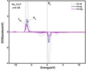
studied the detailed partial densities of states of Fe-3d, Fe-3d (t2g) and Fe-3d(eg) of Ga0.875Fe0.125P under our
discussion and are shown in Fig. 5.
Table 1. Calculated lattice constants, Spin down band gap , Spin up Band gap , Valence band edge
splitting (ΔEC), Conduction band edge splitting (ΔEV) and other parameters of GaP and Ga0.875Fe0.125P.
Compound/ Property
LC (Å) B
(GPa)
ΔEC ΔEV
GaP 5.63
5.516a 5.45b
80.90
76.51a
88.00c
0.859 0.4327
-0.4196
Ga0.875Fe0.125P 5.56 0.5769 0.9970
-0.1196
1.2282 -0.6963
0.2312 -1.3478
-0.9277
a Ref. [26], b Ref.[27], c Ref.[28]
Fig 1. The structural optimization for GaP and Ga0.875Fe0.125P.
1739 | P a g e
Fig 3. Spin-polarised Band Structures and TDOS for spin up and spin down of Ga0.875Fe0.125P.Fig 4. Calculated Partial Density of states of Ga0.875Fe0.125P.
Fig 5. Projected density of states (PDOS) of Fe-3d, Fe-t2g and Fe-eg of Ga0.875Fe0.125P.
IV. CONCLUSION
In the present work, we have calculated the structural and electronic properties of pure GaP and Ga0.875Fe0.125P
in zinc blende phase by first principle DFT calculations using Local density Approximation (LDA)
parameterized by CA as exchange correlation. We investigated that in case of Ga0.875Fe0.125P, P-3p and Fe-3d
states undergo hybridization near the Fermi energy level and due to hybridization between these states, valence
band maximum and conduction band minimum cross the Fermi energy level in majority spin channel and
minority spin channel respectively and show metallic behavior. Calculated results are in good agreement with
1740 | P a g e
V. ACKNOWLEDGEMENT
We acknowledge SIESTA group for this package for support in understanding this siesta package.
REFERENCES
[1] S.D. Sarma, Nat. Mater. 2, 2003, 292.
[2] I. Malajovich, J.J. Berry, N. Samarth, D.D. Awshalom, Nature 411, 2001, 770.
[3] H. Ohno, Science 281, 1998, 951.
[4] H. Akinaga, H. Ohno, IEEE Trans. Nanotechnol. 1, 2002, 19.
[5] S.J. Pearton, C.R. Abernathy, M.E. Overberg, G.T. Thaler, D.P. Norton, N. Theodoropoulou, A.F. Hebard, Y.D.
Park, F. Ren, J. Kim, L.A. Boatner, J. Appl. Phys. 93, 2003, 1.
[6] S.A. Wolf, D.D. Awschalom, R.A. Buhrman, J.M. Daughton, S.V. Molnar, M.L. Roukes, A.Y. Chtchelkanova,
D.M. Tregger, Science 294, 2001, 1488.
[7] I.I. Mazin, Appl. Phys. Lett. 77, (2000), 3000.
[8] I. Zutic, J. Fabian, S.D. Sarma, Rev. Mod. Phys.76, 2004, 323.
[9] A. Iftikhar, B. Amin, Computational Materials Science 68, 2013, 55.
[10] F.J. Owens, A. Gupta, K.V. Rao, Z. Iqbal, J.M.O. Guillen, R. Ahuja, J.H. Guo IEEE Trans. Magn. 43, 2007,
3043.
[11] S.S. Hardev, S. Mukhtiyar, H.R. Ali, K.K. Manish, Journal of Alloys and Compounds, 536, 2012, 214.
[12] T.C. Schulthess, W.M. Temmerman, Z. Szotek, A. Svane, L. Petit, J. Phys. Condens. Matter 19, 2007, 165207.
[13] W. Kohn, S.L. Sham, Phys. Rev. A 140, 1965, 1133.
[14] A. Djedid, B. Doumi, S. Méҫabih, B. Abbar, J. Mater. Sci. 48, 2013, 6074.
[15] C.M. Fang, G.A. de Wijs, R.A. de Groot, J. Appl. Phys. 91, 2002, 8340.
[16] E. Kulatov, H. Nakayama, H. Mariette, H. Ohta, Y.A. Uspenskii, Phys. Rev. B 66, 2002, 045203.
[17] J.B. Gosk, R. Puzniak, G. Strzelecka, A. Materna, A. Hruban, A. Wisniewski, A. Szewczyk, G. Kowalski, K.
Korona, M. Kaminska, A. Twardowski, Supercond. Sci. Technol. 21, 2008, 065019.
[18]. J.M. Solar, E.Artacho, J.D. Gale, A. Garcia, J. Junquera, P. Ordejon, D.Sanchez, J. Physics Condens. Matter.
14, 2002, 2745.
[19] Perdew, Zunger, Local density approximation, Phys. Rev. B 23, 1981, 5075
[20] N. Troullier, J. L. Martins, Phys. Rev. B 43, 1991, 1993.
[21] O. Madelung, Semiconductors: Data Handbook, III ed., Springer-Verlag, Berlin, Heidelberg, New York, 2003
[22] F. Murnaghan, Proc. Natl. Acad. Sci. 30, 1944, 244.
[23] R. Anita, K. Ranjan, Journal of Superconductivity and Novel Magnetism, 30 (6) 2017, 1483.
[24] R. Anita, K. Ranjan, Applied Physics A : Materials Science and Processing 122(8), 2016.
[25] B. Amin, S. Arif, Iftikhar Ahmed, M. Maqbool, R. Ahmad, S. Goumri-Said, K. Prisbre, Journal of Electronic
Materials 40(6), 2011, 1428.
[26] A. Bouhemadou, R. Khenata, M. Kharoubi, T. Seddik, A.H. Reshak, Y. Al-Douri Comput.Mater. Sci. 45, 2009,
474.
[27] J. Heyd, J.E. Peralta, G.E. Scuseria, R.L. Martin, J. Chem. Phy., 123, 2005, 174101.
[28] S.Q. Wang, H.Q. Ye, Phy. Rev. B 66, 2002, 235111.