Saw Filters Vibrational Sensitivity Characterization
Massimiliano Rossi1,†,‡ ID
1 MBDA Italia S.p.A. Via Monte Flavio, 45 - 00131 - Roma - Italy; [email protected]
Abstract:A novel characterization method for discrete saw filters vibrational sensitivity is presented.
1
The proposed approach allows the characterization of filters under vibrations and the extraction of a
2
behavioural model. Filters are assumed to be transducers so that external induced vibrational energy
3
is partially transformed in a undesired simultaneous amplitude and phase modulation of the input
4
RF signal. When the filter is mechanically excited with vibrations, it introduces spurious amplitude
5
and phase modulation to the input signal that can potentially affect the link quality.
6
Keywords:microwave filters; vibration sensitivity; acoustic noise
7
1. Introduction 8
Filtering stages are fundamental blocks in all communication systems from mobile terminals to
9
complex aerospace and defence ones. When volumes and weights are limited and good electrical
10
performance must be guaranteed, a plethora of new technologies seems available to the system
11
designer. Surface Acoustic Wave (SAW) or Dielectric Resonator (DR) filters, for example, appear to
12
be ideal candidates. A big concern arises when severe or very hard enviromental conditions have
13
to be taken into account, such environments are well known in the aerospace and defence fields [1].
14
Besides high temperature variations there is a big concern about the presence of mechanical vibrations
15
even at acoustic frequencies with very high pressure levels. Undesired phenomena generated by
16
vibrations are well known also in crystal oscillators [2] where some fundamental figure of merit
17
are currently available. Vibrational energy can affect the electrical performance of filtering stages
18
introducing spurious signal modulations that can degrade the RF link quality. In this paper it is
19
proposed a novel characterisation method that can be used to model the vibration sensitivity of saw
20
filters when subjected to vibrational energy.
21
2. General theory and characterization technique 22
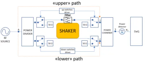
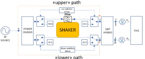
Induced phase noise characterisation methods as well vibration sensitivity figure of merit for filters [3][4] are available, but from these it is not easy to directly infere behavioural models of discrete microwave filters. Usually, manufacturers perform vibration and shock tests according to international standards [5] [6] [7] in order to certify that the devices meet electrical performanceafterthe trials [8], but sometimes evidence of correct operation of the device is requiredduringthe application of the solicitation. A filter subjected to vibrations can be reasonably treated as a transducer so that external induced vibrational energy is partially transformed in simultaneous amplitude and phase modulation of the input RF or IF signal. The signal bandwidth is supposed to be much wider than the vibration induced modulation bandwidth. The theory of operation can be understood by referring to the test-bed reported in Figure1. Using a compact complex envelope notation [9], the RF source generates an in-band CW (Continuous Wave) signal:
ii(t) =Aoejϕo (1)
at nodeAof the circuit where it is splitted in two paths:upperandlower. The signal in theupperpath
Figure 1.Characterisation set-up
flows through the filter where emerges modulated both in amplitude and phase due to the vibrational energy as:
io(t) =AomF(t)e[ϕo+jψF(t)] (2) with 0 ≤mF(t) ≤1. The signal in thelowerpath flows in a through-line and recombines with the signal coming form theupperpath in an isolated RF combiner. The signals flow is regulated by two couples of SPDTs (Single Pole Double Throw) in order to provide high isolations level: the first couple controls theupperpath; the second couple controls thelowerpath. Each couple of SPDT is driven by a dedicated driver. The signal from the output RF combiner is injected in a zero bias schottky detector whose output signal, being eventually conveniently amplified by a low noise stage, is acquired. A dedicated fixture is designed and fixed to the shaker to allow vibration tests to be performed. The filter, generally available in a SMT package (Surface Mount Technology), is soldered over a microstrip circuit with dedicated input and output connectors. A microstrip through line is located near the filter with its own input and output connectors. So, two input ports and two output ports are available on the test jig, each circuit is independent from the other but both shares the same vibrational energy. Following the scheme, it is possible to note that the jig, fixed to the shaker, is connected to the isolated RF power divider and combiner using phase invariant coaxial cables so that when the SPDTs are driven as in Figure2, it is possible to identify anupperandlowerpath where the input signal is first splitted and
Figure 2.General characterisation set-up
then recombined. Using the superposition principle, the input signal to the power detector due to the
upperpath is:
Sout1(t) =AoS3AumF(t)e[jψF(t)+jφ3Au] (3) where:
23
1. S3Auejφ3Au is the transmittance from portAto port3through theupperpath when there is no 24
vibration
25
2. mF(t)ejψF(t)is the instantaneous transmittance of the filter under vibrations andψF(t)is a real 26
valued function
27
while the input signal to the power detector due to thelowerpath is:
where:
28
1. S3Adejφ3Ad is the transmittance from portAto port3through thelowerpath when there is no 29
vibration
30
2. md(t)ejψd(t)is the instantaneous transmittance of the microstrip line under vibration, beingψd(t) 31
a real valued function
32
so, therecombined output signalarising from the RF combiner can be put in the form:
Sout(t) =AoS3Admd(t)e[jψd(t)+jφ3Ad]+AoS3AumF(t)e[jψF(t)+jφ3Au] (5) this signal is injected in a zero bias schottky detector, whose output signal is of the form:
v1(t) =kdPi(t) (6)
wherekdis the detector’s sensitivity andPi(t)the instantaneous power of the RF input signal. When the system is under vibration, the instantaneous output signal is:
v1(t) =A2okd(2S3AdS3Aumd(t)mF(t)cos(ψd(t) +φ3Ad−ψF(t)−φ3Au) +S32Admd(t)2+S32AumF(t)2) (7) while, when no vibrational energy is injected to the system:
v1_static =A2okd(2S3AdS3Aucos(φ3Ad−φ3Au) +S32Ad+S32Au) (8) so,v1_static, is time independent.If the filter’s microphonicity is negligible, the output signal is constant. If the microstrip circuit, that’s part of thelower path, can be assumed to be quite insensible to vibrations, it’s possible to simplify the output signal as:
v1(t) =A2okd(2S3AdS3AumF(t)cos[φ3Ad−ψF(t)−φ3Au] +S32Ad+S23AumF(t)2) (9) now, when the SPDT couple of the down path is driven in order to open the signal’s flow, the test-bed is equivalent to Figure3. The output signal,under vibration, is:
Figure 3.Characterisation set-up withlowerpath opened
v1_down_o_vibr(t) =A2okdS23AumF(t)2 (10) while, in static conditions:
v1_down_open_static =A2okdS23Au (11) when the SPDT couple of theupperpath is driven in order to open the signal’s flow, the test-bed is equivalent to that reported in Figure4. The output signal, under vibration and in static condition, is:
Figure 4.Characterisation set-up with upper path opened
so the filter amplitude modulation, if present, constitutes the signal:
v1_down_o_vibr(t) =A2okdS23AumF(t)2 (13) If the DC component is prevalent, then the amplitude modulation is negligible andmF(t)2∼=1. Under these conditions the signals: v1_down_o_vibr(t),v1_up_o_vibr,v1_down_o_vibr(t) are DC voltages and the phase induced modulation functionψF(t) is recoverable from the output signal:
v1(t) =2A2okdS3AuS3Adcos(ψF(t) +φ0) +A2okdS23Ad+A2okdS23Au (14) apart from a constant phase termφ0=φ3Au−φ3Ad. The vibration induced phase modulationψF(t)is 33
transformed in aamplitude modulationof the low frequency signalv1(t), so a wise choice of the phase
34
termφ0allows to maximize the signal’s dynamic range. If the low signal phase difference between
35
upper and lower pathsφ0= (2n+1)π2 withn∈Z, than the slope of the cosine function in equation
36
(14) is maximized. Changing the vibrational sine frequency, it’s possible to extract the relative induced
37
phase modulation and the characterization process can be fully automated.
38
2.1. System Simulation and Validation 39
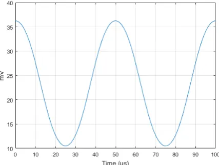
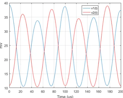
The theoretical approach has been validated through RF system simulations using NI AWR VSS
40
Visual System SimulatorTM[10] and MATLABR[11]. The NI AWR VSS schematic is reported in Figure
41
5and includes, in a more detailed form, the characterisation set-up depicted in Figures3and4. A
Figure 5.Characterisation set-up VSS system model
42
signal generator injects a -10 dBm CW tone at 1 GHz into a power divider where it is divided in two
43
branches. The upper path contains an RF filter, in this case a 3 poles, 10 MHz bandwidth Bandpass
44
Chebyshev type 1 filter with an insertion loss of 3 dB, followed by aphase modulator that represents the 45
induced phase modulation due the vibrational energy. The vibration induced phase modulating signal is a
46
20 KHz unit amplitude sine wave injected in a phase modulator with a phase sensitivity coefficient
47
Kp = 0.1. The presence or absence of vibrations and the path selection is performed by dedicated 48
SPDTs whose insertion loss take into account the additional losses introduced by the cables also. The
lower path contains the dedicated branch selection SPDTs, cable and a RF phase shifter. The signals
50
arising from the upper and lower paths are injected in a RF combiner whose output port is terminated
51
in a power detector. The low frequency signal from the power detector, described by equation (14) is
52
reported in Figure6, the same signal exctracted using the Matlab model is reported in Figure7with an
Figure 6.Low frequency signal from power detector (VSS model) withKp=0.1
Figure 7.Low frequency signal from power detector (Matlab)withKp=0.1
53
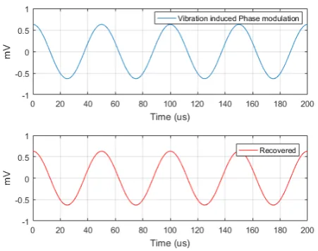
excellent agreement between both models. The induced phase modulating signal and the recovered
54
signal are depicted in Figure8
55
2.2. Extension to weak time-dependent amplitude modulation case 56
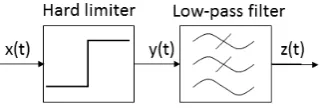
If the induced amplitude modulation is time-dependent, a signal processing approach can be adopted in order to extract the induced phase modulation. IfmF(t)26=1 a more precise technique can be exploited, deleting the DC terms in (9) in post-processing. In fact, looking at Figure9, if a generic low pass signal:x(t) =m(t)cos[ψF(t)]is injected in a hard limiter, the corresponding output signal can be put in the form:
y(t) =sign[m(t)cos(ψF(t))] =
(
+1 for |ψF(t)|< π2 −1 for π
2 <|ψF(t)|<π withsign(x) =
(
+1 ifx>0 −1 ifx<0
Figure 8.Induced phase noise modulating signal and recovered withKp=0.1
Figure 9.Signal processing approach for induced phase modulation extraction
The functiony(t)is periodic inψF, so the corresponding Fourier series expansion can be written as:
y(ψ) =
+∞
∑
n=1,3,5,...
Yncos(nψ) (16)
with coefficients:
Yn=
4 sin nπ2
nπ (17)
a low-pass filter eliminates the high order harmonics so that
z(t) = 4
πcos[ψF(t)] (18)
this allows to easily extract the phase induced modulation function.
57
3. High induced amplitude modulation case 58
When the induced amplitude modulation function mF(t) is not negligible, it is necessary to modify the test-bed in order to be able to extract the phase and the amplitude modulating functions. To this purpose, the output RF combiner is replaced by a 180◦hybrid where two different power detectors are connected to theΣand∆ports. The output signals arising from the power detectors, eventually conveniently amplified by low noise stage amplifiers, are injected in a simultaneous sampling DaQ (Data Acquisition device). Looking at Figure10, if the RF source generates a signal of the form (1), the signals arising from the power detectors are:
v1(t) =kd1A2o
S322 S22A+m2F(t)S231S21A+2mF(t)S31S32S2AS1Acosφup−φdown
(19)
v2(t) =kd2A2o
S422 S22A+m2F(t)S241S12A−2mF(t)S41S42S2AS1Acos
φup−φdown
Figure 10.Extended characterisation set-up
whereS32,S31,S41,S42are the modules of the trasmittances of the 180◦hybrid andS1A,S2Aare the modules of the trasmittances of theupperpath from nodeAto node1andlowerpath from nodeAto node2respectively. In general, the detectors sensitivity coefficients kd1and kd2, the parameters S32, S31, S42, S41are different, even slightly, from each other. Opening theupperpath in static conditions (no vibrations), the output voltages from the detectors are constants, respectively equal to:
v1=kd1A2o
S232S22A=A (21)
v2=kd2A2o
S242S22A=B (22)
closing theupperpath, while opening thelower, the output voltages from the detectors are constants and respectively equal to:
v1=kd1A2o
S231S12A=C (23)
v2=kd2A2o
S241S12A=D (24)
VariablesA,B,C,Dhave been introduced only to simplify the expressions instatic conditionsand allow compact notations. When vibrations are present, and bothupperandlowerpaths are closed, the signals from the detectors are time dependent and respectively equal to:
v1(t) =A+m2F(t)C+2mF(t) √
ACcos
φup−φd
(25)
v2(t) =B+m2F(t)D−2mF(t) √
BDcos
φup−φd (26)
after some algebraic manipulations, it is possible to write:
mF(t) =
1 q C A+ q D B r C A
v1(t)−A
C +
r
D B
v2(t)−B
D ! 1 2 (27)
while the phase induced modulation is:
φup−φd=ψF(t) +φupo−φd=cos−1
v1(t)−A
C −
v2(t)−B D
2mF(t)
q A C+ q B D (28)
Figure 11.Extended characterisation set-up
63
to that reported in Figure5with two main differences: after the RF filter there are two separated
64
amplitude and phase modulators, each of these modulates the RF signal indipendently from the other
65
with different modulation frequencies and modulation indices. The signal travelling the upper path
66
and that travelling the lower path recombines into a 180◦hybrid coupler. TheΣand∆output signals
67
are then injected in two RF power detectors whose output voltages have been stored and processed.
68
The vibration induced phase modulating signal is a 20 KHz unit amplitude sine wave injected in
69
a phase modulator with a phase sensitivity coefficientKp = 0.1.The vibration induced amplitude 70
modulating signal is a 11 KHz unit amplitude sine wave injected in a amplitude modulator with a
71
normalized sensitivity coefficientKm=0.1. The amplitude and phase modulating frequencies are not 72
harmonically related and have been choosen different in order to verify the correct recover of both.
73
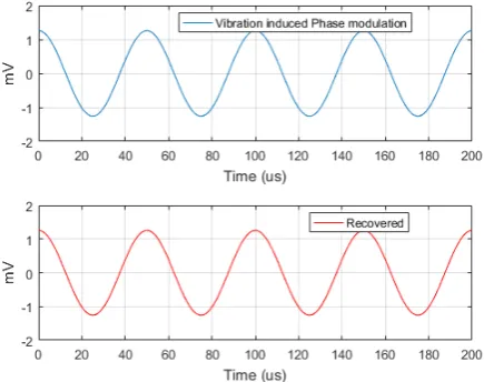
The output voltages from the power detectorsv1andv2under vibrations are reported in Figure12
Figure 12.Low frequency signals from power detectors withKm=Kp=0.1
while the induced amplitude modulating signal and the one recovered are reported in Figure13.
75
The induced phase modulating signal and the one recovered are reported in Figure14. For a fixed
Figure 13.Vibration induced amplitude modulating signals withKm=Kp=0.1
Figure 14.Vibration induced phase modulating signals withKm=Kp=0.1
76
vibrational frequency, a change of the vibrational energy is modeled as a corresponding change of
77
phase and amplitude modulation indices. If the amplitude and phase modulation indices are raised
78
toKm =0.5 andKp =0.2 respectively, the output voltages from the power detectorsv1andv2are
79
reported in Figure15. The induced amplitude and phase waveforms and the recovered signals are
80
reported in Figure16and Figure17. It is noteworthy that the quantities: A,B,C,Dcan be frequency
81
dependent, but all of them can be characterized in the frequency domain, if necessary. The quantities
82
C,Dare also allowed to be temperature-dependent as these are directly related to the transmittance
83
of the filter under test. Moreover, the proposed method does not require a sinusoidal vibrational
84
spectrum in order to extract the amplitude and phase induced modulations, but it can be theoretically
85
arbitrary.
Figure 15.Low frequency signals from power detectors withKm=0.5 andKp=0.2
Figure 16.Vibration induced amplitude modulating signalsKm=0.5 andKp=0.2
4. System Sensitivity Considerations 87
All the schemes discussed in previous sections works at high Signal to Noise Ratios by design, insertion losses of the devices are quite small even that of SAW filters (usually≤10 [dB]). The input signal is provided by a RF source with a very high SNR while power detectors operate with signal levels≈40 [dB] higher their typical tangential sensitivity [12]. Limiting the analysis to the induced phase modulation recovering, it is possible to focus the attention to equation (14) reported below for convenience, in order to derive some considerations.
v1(t) =2A2okdS3AuS3Adcos(ψF(t) +φ0) +A2okdS23Ad+A2okdS23Au (29) If the termφ0=−π2, than it is possible to write
v1(t) =2kdA2oS3AuS3Adsin(ψF(t)) +A2okdS23Ad+A2okdS32Au (30) the induced phase modulationψF(t)can be assumed to beψF(t) =2πKpcos(2πfmt), being fmthe vibration frequency. As vibrational induced phase modulation comes from low frequency mechanical excitation (sometimes up to acoustic frequencies), it is reasonable to suppose [13] that the bandwidth
BW of the signal (29) is limited toBW ≈ 2 2πKp+1fm < 100 [KHz]. The estimated SNR at the output port of the RF combiner (or the output ports of the 180◦hybrid) is reported in Figure18. It can be assumed that the low frequency signal, acquired by the DaQ, is mainly contaminated by thermal noise coming from the RF section and by the intrinsic thermal noise of the device. The noise power from RF stages isPnRF ≈-124 dBm corresponding to a RMS noise voltageVnRF ≈0.28µV. The RMS
noise voltage of a DaQ is tipically much higher. For example, the National Instruments 6356 [14] in the smallest input voltage range, is characterized by a RMS noise voltageVn ≈61µV, so it is prevalent over the contribution due the RF section. Small values ofKppush the system to the limit of sensibility
Figure 18.SNR at the output ports of the 180◦hybrid
asv1(t)tends to a DC value, but at the same time,makes the filter able to operate in a severe environment. IfKpis small, it is possible to approximate the sine function in equation (30)
v1(t)≈4kdA2oS3AuS3AdπKpcos(2πfmt) +A2okdS23Ad+A2okdS23Au (31) the signals measured experimentally can be written as:
4π qv∗
1_up_o_staticv
∗
1_down_o_static
=Kpcos(2πfmt) +n (35)
beingna gaussian noise contribution with powerPn=σ2. In this case, a powerful tool is represented
88
by the FFT (Fast Fourier Transform). If the DaQ operates at a sample frequency of fs[Hz] and N 89
samples are acquired for each signal, the FFT of the signal reported in equation (35) generates N2
90
points in the frequency domain where every frequency "bin" is fs
M [Hz] wide. A Matlab simulation has 91
been used to estimate the parameterKpwith a relative errore≤1% in order to define the minimum
92
detectable phase sensitivity coefficientKpmin. The vibrational frequency has been set fm=10 [KHz] 93
with a DaQ sample frequency fs=1 [MHz]. The effective systemSNRdB=10 log
K
P2
2σ2
−Gpwhere 94
KP2
2 is the signal power andGp=10 log
N 2
the processing gain of the FFT. The magnitude of the
95
spectrum at the frequency "bin" corresponding to the vibrational frequency has been calculated while
96
sweeping the parameterKp, thus changing the SNR of the system and determining the relative error; 97
the procedure has been iterated in order to obtain a distribution of the error. Some amplitude spectra
98
are reported in Figure19for different values ofKpwhile in Figure20is reported the histogram fit of 99
the relative error distribution (nearly gaussian) corresponding to the identified minimum detectable
100 Kp.
Figure 19.Amplitude spectra of signal (35) for different values ofKp
Figure 20.Histogram fit of the relative error distribution
From simulations it has been found a minimum detectable phase sensitivity coefficientKpmin ≈ 102
2·10−4[rad/V] with relative errorse≤1% within 3σKp. 103
5. Conclusion 104
In this paper it has been derived low-cost characterisation techniques for discrete filters under
105
vibrations. The methods allows the extraction of both the vibration induced amplitude and phase
106
modulation using scalar measurements only. The first technique requires few components, but is
107
suitable for filters that exhibit negligible amplitude induced modulation. The second, more powerful
108
and general, requires two independent power detectors that do not have to be matched. It is noteworthy
109
to note that the proposed characterization methodology is theoretically inherently robust against the
110
RF generator phase noise. The signals extracted by the RF power detectors depends on thedifference 111
between the phases of the upper and the lower paths thus erasing spurious contribution coming
112
before the first power divider. The proposed approaches allow to characterize a microwave filter
113
under vibrations, but also to derive behavioural models that can be used to simulate a RF chain where
114
vibrational induced phenomena are taken into account.
115
Conflicts of Interest:The author declare no conflict of interest 116
References 117
1. MIL-STD-810G: "Environmental Engineering Considerations and Laboratory Tests",Department Of Defence Test
118
Method Standard, 2014 119
2. R. L. Filler, "The acceleration sensitivity of quartz crystal oscillators: a review," in IEEE Transactions on 120
Ultrasonics, Ferroelectrics, and Frequency Control, vol. 35, no. 3, pp. 297-305, May 1988. doi: 10.1109/58.20450 121
3. Hati, A.; Nelson C.W.; Howe D.A.: ‘Vibration-Induced PM and AM Noise in Microwave Components’,IEEE
122
Transactions on Ultrasonics, Ferroelectrics, and Frequency Control, 2009, Volume: 56, pp.2050-2059 123
4. A. Hati; C. W. Nelson; D. A. Howe; N. Ashby; J. Taylor; K. M. Hudek; C. Hay; D. Seidel; D. Eliyahu : ‘Vibration 124
Sensitivity of Microwave Components ’,2007 IEEE International Frequency Control Symposium Joint with the 21st
125
European Frequency and Time Forum, 2007, pp.541-546 126
5. Locke, S.; Sinha B.K.: ‘Acceleration and Vibration Sensitivity of SAW Devices’,IEEE Transactions on Ultrasonics,
127
Ferroelectrics, and Frequency Control, 1987, Volume: 34, pp. 29-38 128
6. IEC 60068-2-6:2007: "Environmental testing – Part 2-6: Tests – Test Fc: Vibration (sinusoidal)", Edition 7.0 date: 129
2007-12 130
7. IEC-60068-2-27:2008: "Environmental testing – Part 2-27: Tests –Test Ea and guidance: Shock", Edition 4.0 date 131
14. National Instruments 6356 DaQ,http://www.ni.com/nisearch/app/main/p/ap/tech/lang/en/pg/1/sn/ 141