ISSN: 2319-8753
International Journal of Innovative Research in Science,
Engineering and Technology
(An ISO 3297: 2007 Certified Organization)
Vol. 3, Issue 10, October 2014
Design and Verification Serial Peripheral
Interface (SPI) Protocol for Low Power
Applications
S. Choudhury, G.K.Singh, R.M.Mehra
Department of Electronics and Communication Engineering, School of Engineering and Technology, Sharda University, Greater Noida, India
ABSTRACT: Serial peripheral interfaces (SPI) are widely used to provide economical board level interfaces between different devices such as microcontrollers, Digital to Analog Converter’s, Analog to Digital Converter’s and other. Many Integrated Circuit manufacturers produce components that are compatible with SPI. Serial communication is the process of sending data one bit at a time, sequentially, over a link. A serial connection requires fewer interconnecting cables (e.g., wires/fibers) and hence occupies less space. For high performance systems, FPGAs (field programmable gate arrays) also uses SPI to interface as a slave to a host, as a master to sensors. In this work, an approach is proposed for the design and verification of configurable Intellectual Property (IP) module of Serial Peripheral Interface (SPI) protocol using Verilog and System Verilog.
KEYWORDS: Serial peripheral interfaces (SPI), SPI Control register, Verilog and System Verilog.
I. INTRODUCTION
Serial to Peripheral Interface (SPI) technology was developed to replace parallel interfaces so that we don’t have to route parallel bus around PCB and provides high speed data transfer between the devices. Motorola was the first company that named SPI to a circuit technique used in the late 1970s in its first 68000 based microcontroller unit to connect it to peripheral functions and later adopted by others in the industry. SPI become a popular communication protocol because of its simplicity of interfacing and the speed that allows communication of transferring data easily. SPI has earned a solid role in embedded systems whether it is system on chip processors, both with the higher end 32 bit processors such as those using MIC, power PC or ARM and with other microcontrollers such as PIC, AVR. Usually SPI controllers are included on these chips and are capable of running in either master mode or slave mode. Field programmable gate array or chip based designs sometimes use SPI to communicate. So nowadays SPI is a common technology used for communication with peripheral devices where data needs to be transfer speedily and within real time constraints [1-5].
Intel is currently developing a successor to its low pin count (LPC) bus known as Enhanced Serial Peripheral Interface bus (eSPI). The enhanced SPI was made with an aim to allow reduction in the number of pins required on motherboard compared to systems using low pin count, more throughput than LPC, reduce the working voltages to 1.8 volts to facilitate smaller chip manufacturing processes, allow enhanced SPI to share serial peripheral interface flash devices with the host whereas on the other hand low pin count (LPC) bus did not allow firmware hubs to be used by LPC peripherals and enhanced serial peripheral interface also allow system designers to trade off cost and performance. To save pins the enhanced serial peripheral interface bus can either be shared with SPI devices or be separate from the SPI bus to allow more performance.
ISSN: 2319-8753
International Journal of Innovative Research in Science,
Engineering and Technology
(An ISO 3297: 2007 Certified Organization)
Vol. 3, Issue 10, October 2014
protocols for both inter-chip and intra-chip low/medium speed data-stream transfer [5]. It is also a popular interface used for connecting peripherals to each other and to microprocessors [11].
K. Aditya etal reported that the Synchronous serial interfaces are widely used to provide economical board level interfaces between different devices. The SPI master core consists of three parts, Serial interface, clock generator and Wishbone interface. The main objectives of this specification are to create a flexible interconnection means for use with semiconductor IP cores. This allows various IP cores to be connected together to form a System-on-Chip and to make WISHBONE interfaces independent of logic signaling levels [6-7].
As we know that UART protocol has been used frequently for short distance off-board data transfer, software debugging etc. The ever increasing complexity of the processing system to design, the modular approach has become a must. With these goals in mind, Abdul [29] have designed a UART-to SPI core which can be used as a module in building bigger systems incorporating the UART protocol as their serial communication protocol and SPI as Serial bus for data transfer [9].
The designed SPI is used for communication between different peripherals with that of a processor in a SoC (system on chip) application and also SPI Protocol is used in Real Time application of a SoC (System on chip) in order to communicate with the PPC 440 Processor and other peripherals which is applicable for present day Avionics Systems in Defences [15].
II. FUNCTIONDISCRIPTION
The SPI system provides a simple method for a master and a selected slave to exchange data serially. The system is enabled by setting the enable bit (SPIE) of the control register.
The four SPI port pins which are associated with the SPI functions are as follows: • MOSI - Master out - Slave in
• MISO - Master in - Slave out • SCK - Serial clock
• SS - Slave select
Fig 1: Block Diagram of SPI
ISSN: 2319-8753
International Journal of Innovative Research in Science,
Engineering and Technology
(An ISO 3297: 2007 Certified Organization)
Vol. 3, Issue 10, October 2014
Clock phase and clock polarity control bit in the control register selects one of four possible clock formats to be used by the SPI system. Clock polarity bit selects an inverted or non-inverted clock. On the other hand clock phase bit is used to accommodate two fundamentally different protocols by sampling data on the leading or trailing edges of the serial clock. The system can be configured as a master or as a slave.
A.MASTER CODE
When the MSTR bit in the control register of the SPI is set to one the master mode is selected. Master SPI module can only initiate transmissions. The data written on the data transmit register is immediately transferred to the shift register when the shift register is empty for the transmission process. The data written could be 8,16,32 bit wide and the bits begins shifting out on the MOSI (master out- slave in) under the control of the SCK generated. The prescaler register is used to determine the speed of the transmission. The SCK (serial clock) pin is the SPI clock output and through this pin the prescaler of master control the shift registers of the slave peripheral. In master mode MOSI (master out-slave in) pin is used to send the data and MISO (master in –slave out) pin is used to receive the data. The slave-select register is used to select the slave with which the master will communicate. If the SS pin of the master tries to become active low then the mode fault error flag will be high if the transmission is in process. If the transmission was not in process then the MSTR bit will be set to logic zero and the system now will be configured as a slave. The transfer operation will depend on the clock phase and clock polarity defined by the CPHA and CPOL bits in the control register.
Fig 2: SPI Core in a Multi-Slave environment
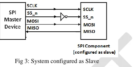
B.SLAVE CODE
The SPI will be configured as a slave when the MSTR bit in the control register will be set to logic zero. In this mode SCK (serial clock) is the SPI clock input from the master, MISO (master in slave out) pin will work as a data output pin and MOSI (master out slave in) pin will work as a serial data output pin. The SS (slave-select) pin will work as an input. The SS pin of the SPI must be asserted low to initiate a transmission and must remain low until the transmission is complete. If SS goes high, the SPI is forced into the idle state and if the slave is not selected means SS is high, then the SCK (serial clock) input is ignored and because of which internal shifting of shift register does not takes place. Some SPI peripherals are capable of only receiving data when configured as a slave and for these kinds of SPI peripheral devices there is no serial data out pin.
If the clock phase bit of the control register is set to logic zero then the odd numbered edges on the serial clock input causes the data at serial data input pin to be latched and on the other hand even numbered edges causes the value previously latched from the serial data input pin to shift into the shift register of SPI and that bit could be LSB or MSB depending on the LSB/MSB bit of control register.
ISSN: 2319-8753
International Journal of Innovative Research in Science,
Engineering and Technology
(An ISO 3297: 2007 Certified Organization)
Vol. 3, Issue 10, October 2014
pin. When CPHA is set to one the first edge gives the first data bit onto the serial data output pin. The transmission complete flag in the SPI status register is set to denote the completion of transfer.
Fig 3: System configured as Slave
During an SPI transfer, data is simultaneously shifted out serially (transmitted) and shifted in serially (received). SCK (serial clock) line synchronizes sampling and shifting of the information on the two serial data lines that are MOSI and MISO. Individual selection of slave SPI device is done by slave select line and the slave devices that are not selected do not interfere with SPI bus activities.
III. FUNCTIONALVERIFICATION
The functional Verification plan of SPI is based on the System Verilog Hardware Verification Language and the methodology used for verification is constraint random coverage driven verification. The verification plan is used to determine the progress and completion of the verification phase of verification and it can be defined as the focal point for defining exactly what needs to be tested. It will verify the design functionally with all possible cases of the protocol. Structure of the verification environment is defined by the verification plan.
Verification environment contains the instances of the entire verification components and there connectivity. To build the verification environment, test bench components based on the configuration needs to be connected and allocated. A test bench component is one that only exists in the test bench and not the part of the physical components in the design that are built with RTL code. For a robust verification environment detailed test bench architecture is essential. This section will describe each component of the test bench, how they are connected and various topologies, various techniques that are used.
ISSN: 2319-8753
International Journal of Innovative Research in Science,
Engineering and Technology
(An ISO 3297: 2007 Certified Organization)
Vol. 3, Issue 10, October 2014
Fig 4: Verification Environment
A generator is used to create a transaction and then randomizes it and puts it in to the driver. Generators create inputs at a high level of abstraction. The driver receives commands from the generator and translates the operations into the actual inputs for the design under verification. It is a class which generates the packets and then drives these packets to the DUT (design under test) input interface.
The driver part of verification deals with the configuration of several registers which are used in data transmission. The outputs from the driver are sent to the DUT (design under test) and to the scoreboard. Monitor identifies all the transactions and reports the protocol violations. It can be categorized into two parts that are passive and active. Passive monitors do not drive any signal whereas on the other hand active monitors are the one that drive the DUT signals. Sometimes monitor can also referred to as receiver.
Monitor receives signals from the design under test and converts the state of the design and its output to a transaction abstraction level so that it can be sent to score-board and stored there in the database to be checked later on.Score-board contains model and the checker in it. It has two inputs one from the driver and the other from the monitor. Monitor only monitors the interface protocol and doesn’t check whether the data is same as expected data or not, as interface has nothing to do with the data.
Checker does the function of unpacking, which is reverse of packing operation that is converting the low level data into high level data. The comparison state is sent to scoreboard and it displays the result after comparison between model and the input taken from monitor.
Interface is used to connect the test bench to the design under test and can be named as bundle of wires (for example it can be thought of connecting two hardware unit blocks with the help of physical wires). Interface can add new connections easily and port lists are compact and carries directional information. The data type for the signals should be logic for the interface instance to be used in the program block. By declaring signal as logic will add flexibility as logic type signals can also be driven by a continuous assignment statement. In case of single drivers signal should be declared as logic whereas on the other hand if the signal is bi-directional that is in out or has multiple drivers then the signal must be declared with a wire data type or any other form of wire data type.
IV. RESULTS&DISCUSSION
ISSN: 2319-8753
International Journal of Innovative Research in Science,
Engineering and Technology
(An ISO 3297: 2007 Certified Organization)
Vol. 3, Issue 10, October 2014
Fig 5: Simulation result when CPHA and CPOL both are low and LSB transmission
The simulation results generated by Questa Sim 10.0b when CPHA (clock phase) and CPOL (clock polarity) both are low is shown in Fig.5. The serial clock generated in this case will be low in idle state as the CPOL is low and sampling will be done on the trailing edge and setup on the leading edge as the CPHA is low. In this case LSB transmission is done as LSB/MSB bit of the control register is set to one.
Fig 6: Simulation result when CPHA and CPOL both are high and MSB transmission
ISSN: 2319-8753
International Journal of Innovative Research in Science,
Engineering and Technology
(An ISO 3297: 2007 Certified Organization)
Vol. 3, Issue 10, October 2014
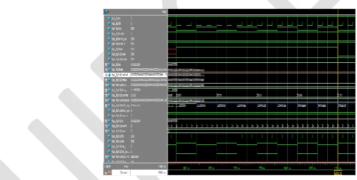
Fig 7: Simulation result when CPHA and CPOL both are low
Figure 7 contains the simulation results generated by Questa Sim 10.0b when CPHA (clock phase) and CPOL (clock polarity) both are low. The serial clock generated in this case will be low in idle state as the CPOL is low and sampling will be done on the trailing edge and setup on the leading edge as the CPHA is low and the value of the data transmit register is 10010010
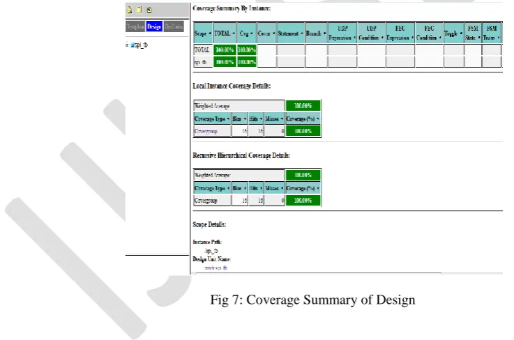
The functional coverage reports of SPI using Questa Sim 10.0b are shown in Fig 8 in various formats.
ISSN: 2319-8753
International Journal of Innovative Research in Science,
Engineering and Technology
(An ISO 3297: 2007 Certified Organization)
Vol. 3, Issue 10, October 2014
Fig 8: Coverage report showing number of bins with names
Coverage report of design shows that our design and verification environment covered 100% functionality in accordance with the design specification as shown in Fig 7.
V. CONCLUSION
We presented the implementation and verification of a Serial Peripheral Interface. A designing and verification of configurable intellectual property (IP) module of SPI protocol using Verilog HDL for implementation part and System Verilog for verification have been shown. We have discussed about the requirement and advantages of serial communication and what are the problems with the serial ports and how Serial Peripheral Interface (SPI) overcomes those problems. After that we have described the general introduction to the SPI.
The basic functionality and operation of SPI and description of registers, signals, pin is discussed. It describes that how we can create serial communication environment between the master and the selected slave device. Functional verification of SPI contains the description of verification platform using System Verilog for the design under test (DUT) that is SPI. In accordance with the design specification we created the verification environment to validate the functionality and operation of configurable intellectual property SPI.
Future scope of the SPI device through Register transfer level modelling which will define the implementation details of the device. After Register Transfer Level modelling, the functional model can be implemented either using the standard digital elements available in the technology library or the FPGA chips available in the market.
ACKNOWLEDGEMENT
The author wishes to thanks Sharda University, Greater Noida, Delhi NCR, India for encouragement and support.
REFERENCES
[1] Pachler, W. ; Pressel, K. ; Grosinger, J. ; Beer, G. ; Bosch, W. ;Holweg, G. ; Zilch, C. ; Meindl, M.A novel 3D packaging concept for RF powered sensor grains, Electronic Components and Technology Conference (ECTC), 2014 IEEE 64th , PP: 1183 – 1188, 2014
[2] Das, R, Singh. G.K., Mehra. R.M.,“Two-Phase Clocking Scheme for Low-Power and High-Speed VLSI”, International Journal of Advances in Engineering Science and Technology, Volume 2, Number 2, 2013.
[3] Bais, A, Singh. G.K., Mehra. R.M.,“ “Design of 6-T SRAM Cell for enhanced read/write margin”, International Journal of Advances in Electrical and Electronic Engineering, Volume 2, Number 2, 2013.
[4] Simon Srot. “SPI Master Core Specification”,Rev.0.6. May 16, 2007.
ISSN: 2319-8753
International Journal of Innovative Research in Science,
Engineering and Technology
(An ISO 3297: 2007 Certified Organization)
Vol. 3, Issue 10, October 2014
[6] Tianxiang Liu ”IP Design of Universal Multiple Devices SPI Interface” IEEE.978-1-61284-632-3, 2011
[7] Specification for the “WISHBONE System-on-Chip (SoC) Interconnection Architecture for Portable IP Cores” Revision: B.3, Released: September 7, 2002.
[8] K. Aditya, M. Sivakumar, Fazal Noorbasha, T. Praveen Blessington, “Design and Functional Verification of A SPI Master Slave Core Using System Verilog”, (IJSCE) ISSN: 2231-2307, Volume-2, Issue-2, May 2012
[9] S.Sarns and J. Woehr, “Exploring I2C,” Embedded Systems Programming, vol. 4, p. 46, Sept. 1991.
[10] F.Leens, “An Introduction to I2C and SPI Protocols,”IEEE Instrumentation & Measurement Magazine, pp. 8-13, February 2009. [11] Freescale Semiconductor, Freescale SPI Block Guide V04.01 , October 14).2008
[12] L. Bacciarelli et al, “Design, Testing and Prototyping of a Software Programmable I2C/SPI IP on AMBA Bus,” Conference on Ph.D. Research in Microelectronics and Electronics (PRIME'2006), pp. 373- 376, ISBN: 1-4244-0157-7, Ortanto, Italy, June 2006.
[13] A.K. Oudjida, Yasmine Hammamet, Tunisia. et al, “FPGA Implementation of I2C and SPI Protocols: A Comparative Study”. Proceedings of the 16th edition of the IEEE International Conference on Electronics Circuits and Systems ICECS, pp. 507 -510, ISBN: 978-1-4244-5091-6, December 13-16 2009,
[14] IP Design of Universal Multiple Devices SPI Interface Tianxiang Liu1, Yunfeng Wang1 * Department of Electronic Engineering, Xiamen University,2011 IEEE.
[15] AnanthulaSrinivas, M.Kiran Kumar , Jugal Kishore Bhandari “Design and Verification of Serial Peripheral Interface”, ISSN: 2321-9939 IJEDR [16] Prophet, Graham. Communications IP adds SPI interface to FP-GA. EDN, v 48, n 27, Dec 11, 2003. www.opencore.org.Simon Srot. SPI Master
Core Specification, Rev.0.6. May 16, 2007
[17] M.Sandya1, K.Rajasekhar, “Design and Verification of Serial Peripheral Interface”, International Journal of Engineering Trends and Technology- Volume3Issue4- 2012
[18] SPI Block Guide V03.06 , Document number S12SPIV3/D , Original Release Date: 21 JAN 2000 , Revised: 04 FEB 2003 , MOTOROLA INC. [19] LogiCORE IP XPS Serial Peripheral Interface (SPI) – V2.02a, DS570 June 22 , 2011 , XILINX
[20] M68HC11 Reference Manual, Inc 2002, 2007 Copyright FREESCALE SEMICONDUCTOR [21] ATmega8_L_Datasheet , 2486AA–AVR–02/2013 , ATMEL
[22] Verilog HDL by Samir Palnitkar Publisher: Prentice Hall PTR (January 15, 1996)
[23] B.Roy,Platform-Independent Customizable UART Soft-Core ,Intelligent Systems, Modelling and Simulation (ISMS), IEEE Third International Conference 2012.p 692-694.
[24] Abdul Ikram, T.Muni Kumar,“Customizable Uart To Spi Ip Core” Vol.1, Issue.2, 2013, ISSN: 2321-7758